 Pamungkas Sumasta
-
1Make up your mind
The Choice is Yours
Before delving into the process of constructing your Generative Kaiboard, it's essential to consider the approach that best aligns with your preferences and objectives. You have three distinct options to choose from in my opinion:
- Full duplication.
- Custom modification.
- Full transformation.
As the name suggests, the first option, full duplication, involves using all the design files provided, ordering the necessary components, and assembling the Generative Kaiboard. This approach is likely to demand the least effort upfront. However, it's essential to be aware of the associated factors, including costs and the possibility of minor adjustments needed in the design.
The second option allows for custom modifications to the existing design, both in terms of PCB design files and the mechanical housing. For PCB design, you'll require an Altium Designer license and some familiarity with the tools, which, unfortunately, isn't entirely cost-free. However, reaching out to Altium might grant you a limited-time trial license. Their customer support is helpful in this regard. Similarly, for housing parts, you can make alterations to the current design, although it's presently created in Siemens NX, which isn't freely available. Nonetheless, you might be able to work with exported files such as STEP and STL. This option is preferable when you wish to refine the design, rectify minor errors, or add personalized elements like your name or logo.
The third and final option is for those with the time, dedication, and willingness to thoroughly study the design, make substantial modifications, and execute them. One advantage here is that you don't necessarily need an Altium license or Siemens NX. You can recreate the schematic drawing in free CAD software like Kicad. It's possible that conversion tools are available to transition from Altium Designer files to Siemens NX. If you're proficient in Kicad, I'd love to hear from you. Opting for a full transformation not only allows for fine-tuning details but also opens the door to incorporating additional unique features that weren't part of the original GKV1 design.
Ultimately, the choice is yours. In this guide, I'll primarily focus on providing build instructions for the duplication method. I'll highlight essential considerations, cost-saving tips, and other factors to be mindful of during this journey. Please keep in mind that duplication does come with its own set of implications, which we'll revisit in the next section below.
Best of luck!
-
2Acknowledge the BOMs, Tools and Skills required
The Bill-of-Materials
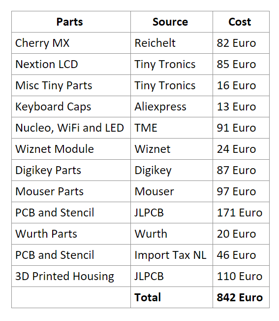
I will say it straight away: duplicating this project is not cheap. It is unfortunately not for the penny-pincher who'd like to save some money by building it's own cool keyboard. You can probably get away with very decent keyboard by spending just a tenth of this project cost. However having said that, that does not mean you have to follow my guide 100%, there are certainly cost optimization strategy you can do. In any case you have to be aware of that.
As a baseline, I started quite from a scratch, I ordered most of the parts for this. Fortunately I had some generous free samples from Wurth Elektronik too which counts for 40% of Electronics BOM. Even with that it still costed me an upwards of 800 Euro as you can see from the preview below:
As you might have guessed, certainly that cost does not 100% reflect the cost of 1 unit. Some components I purchased in a quantity e.g. the PCBs but some like the cherry mx key switches and the 3D printed housing I only purchased enough to built 1 unit. The list above is just a ballpark estimation. On the next step I'll go a bit deeper what you can do to optimize the cost by choosing alternatives etc.
The Tools
I don't really consider this project mandates special tools that you need to have. Apart from typical stuff you'll find on a electronics workbench e.g. Soldering iron with it's companions parts and hot air reflow gun. The need of microscope it is also dependent on your ability, but I've prescribed the board to mostly use 0603 parts and perhaps just a few 0402 so handling it with a naked bare eye should be doable for many people.
As the board prescribe the use of Nucleo board as well as W5300 TOE shield, you don;t necessarily need to worry about soldering fine pitch component yourself. Perhaps apart from Time-of-flight sensor where you'd need to use a hot air gun as the footprint is an LGA.
However, having said that, as majority of the SMT parts are mounted on the top, it is highly recommended that you use a bit more automatic reflow oven. Which means you need to order the stencil and have some affinity with manual screening of a PCB. Honestly myself I did a hybrid, I did both stencil screening and manual hand soldering, I'll detail that on the next step.
The Skills
This project is not for complete beginners I must say upfront. You need to have some affinity with soldering or access to someone that can help you at least. Sure, I tried my best not to use component that is really difficult to manage e.g. BGA, but still soldering an SMT parts is often not as easy as it seems. Not only proper tools is needed but also some experience and some experience with debugging in case some things don't work. Alternatively to the extreme, you can perhaps also ask a fabrication house to do a turn-key assembly for you, such that you don't have to touch a soldering iron at all. This is likely gonna cost you some effort and cost upfront, perhaps some experience in dealing with PCB Assembly, but I guess that'd worth the investment. I'm aware PCBWAY and JLPCB already have that service for a while now, so something to consider.
-
3Parts Selection and Ordering
Parts Selection
I would say in general there are four categories of parts that you need to manage where some are customizable ordering-wise while others are fixed.
- The PCBs
- The Electronics BOM
- The Miscellaneous BOM
- The Housing
The PCBs
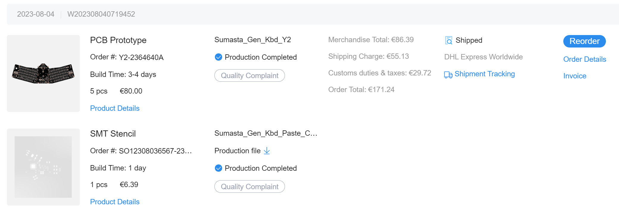
Honestly the PCB is the single part that likely gonna cost you the most. Mainly because the current board dimensions is a bit more than half-a-meter and it is a 4 layer board. The PCB were design without any specific requirements that is going to increase your PCB cost significantly, the hole size, minimum pitch etc should be easy enough for more PCB manufacturer to produce your board hence not increasing the total cost. In my case I ordered from JLPCB as it appeared to be the cheapest with reasonable lead-time. As you can see in the preview below, for 5 pcs it costed me about 86 Euro, all in including shipping etc, double that.
Furthermore, in my case I ordered the PCB in black which is surely not the cheapest option, you can safe some bucks by selecting a green solder mask for instance. Feel free also to benchmark another alternative supplier such as PCBWAY they might have a better deal too. On top of that the bulk of the cost was entirely for shipping and taxes which perhaps you can safe/avoid by choosing different delivery methods.
Another crucial thing that you should not forget is the stencil ordering, assuming that you are planning to assemble it semi-automatic with a reflow oven. In that case you need to include the stencil as well in the order as you can see above it only costed me 6 euro. HOWEVER, you have to take care that the stencil I ordered is a cropped version and only cover the top side, in particular the middle one. The main reason for me is simply the cost, especially the shipping cost too.
You know the PCB dimensions is a bit more than half a meter in length, that means if you want to order the stencil for that size, the stencil dimension and frame must be larger than that, which is acceptable. however from what I see if you want to ship the stencil with that dimensions it is going to cost you a lot of money especially with DHL. That's why as a plan B, I decided to crop the middle part of the PCB where majority of the SMT parts are located, ordered that small cut section, screen and reflow it afterwards the rest of the parts I solder it manually myself.
The Electronics BOM
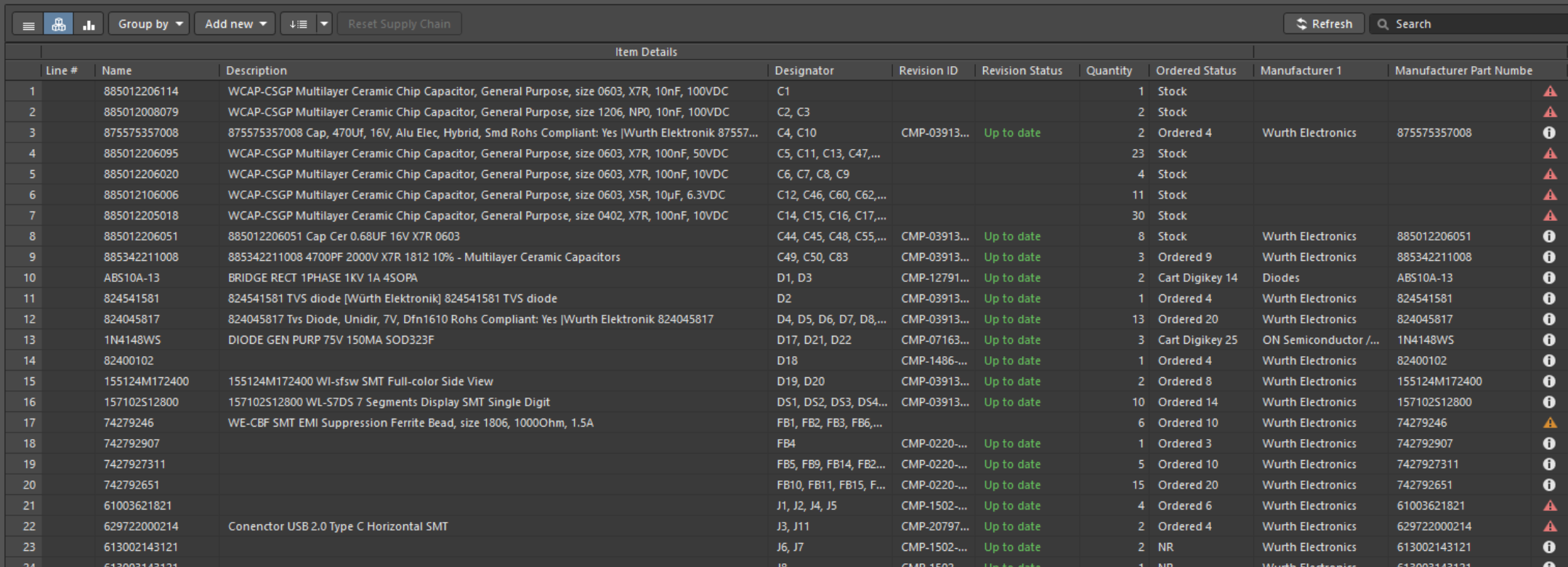
The next thing to manage is the ordering of the Electronics BOM, a.k.a the components that you'll need to solder on the PCB. Surely for some parts you can opt for an alternative e.g. the passive component, but others such as IC and sensor you might not be able to identify the alternative. I publish the complete EBOM both in this Hackaday page as well as in my Github BOM folder. By using the part number you can decide for yourself where to source the parts, and supplier benchmarking tools e.g. findchips or octopart will definitely help you there. In my .xlsx bom sheet you can also see there where I sourced the parts from at the time of building my GKV1.
As I said earlier, majority of EBOM parts are from Wurth Elektronik, they have an amazing web ordering and sampling system where you can easily order and or request sample. For example if you want to get a sample of the PoE Magjack that I use, you can add to cart for a sample here, explain the project, fill the form etc and if all good in a matter of days it should come to you. Apart from the world-leading quality of their components and their free sampling generosity, they also manage a component library for all their parts. In my case their Altium library really did help me a lot. Imagine if I have to build the component footprint etc all by myself in a matter of 1-2 weeks.
The Miscellaneous Parts
On top of the Electronics BOM, there are also some parts that is not necessarily listed in the EBOM files but you will definitely need it. The parts I'm referring too are like the keycaps, the rocket-switch, thumb-cap for the joystick and also including the Nucleo board and LCD. You can leverage your free-will here on some parts e.g. the type of key-caps for your keyboard or the color of the thumb-cover on the joystick but some parts e.g. the Nucleo board and the LCD I suggest you better stick with what I've prescribed. Well unless you prefer to go to the more advance route.
Likewise, the list of the miscellaneous parts you should be able to find in this Hackaday page or on my Github.
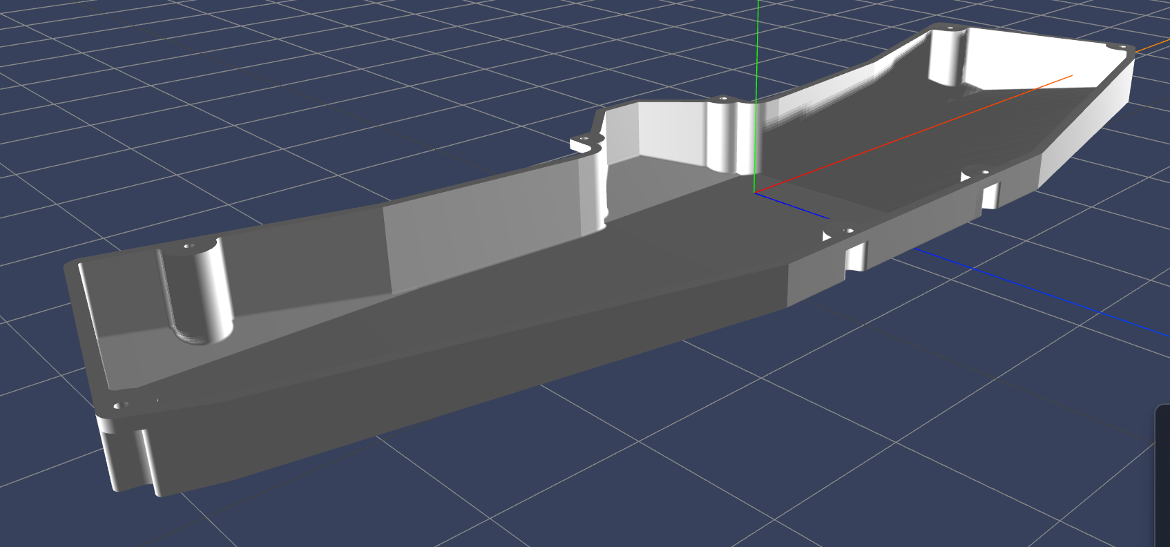
The Housing
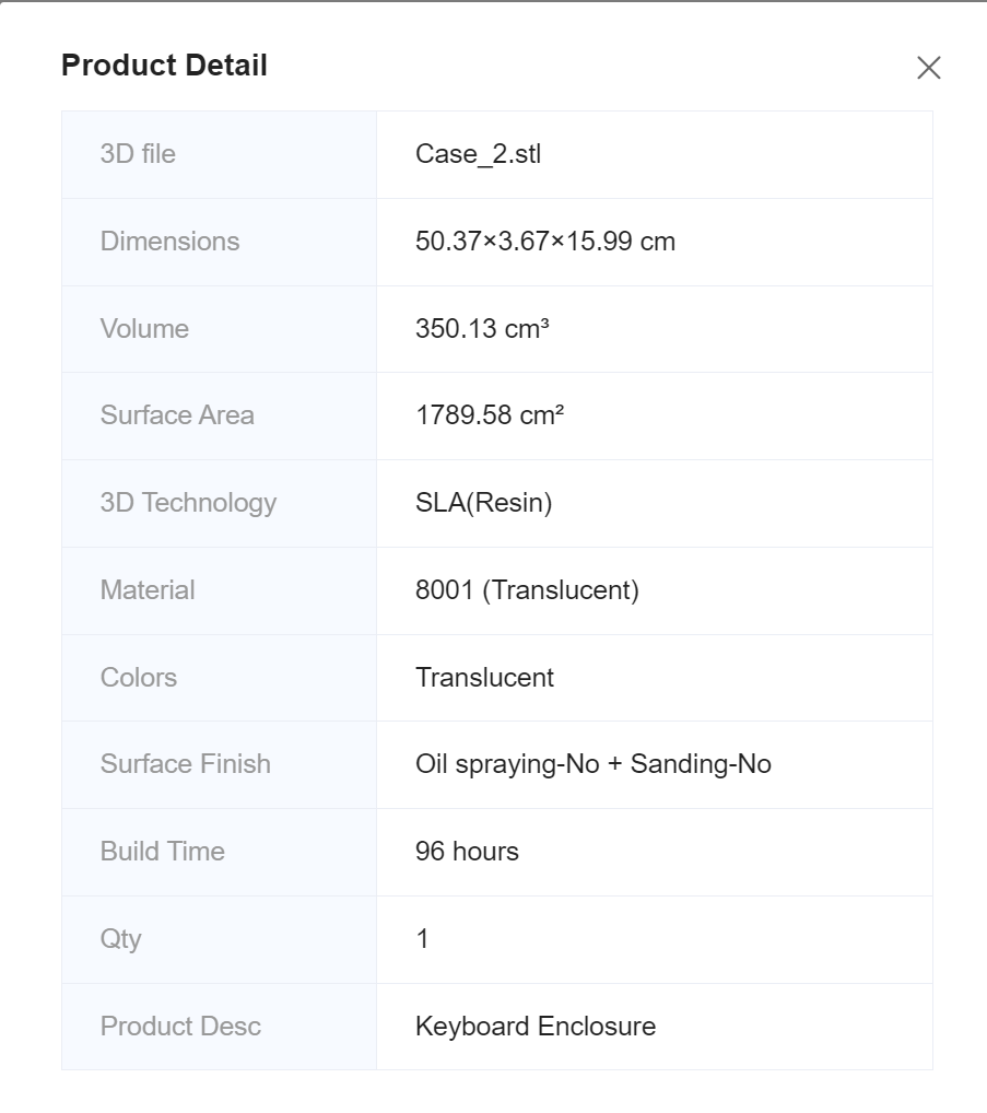
Last but not least I reckon you'd also need a back-housing for your built. This is also the part where you can put out some customization if you will. In my case, I wanted to have it in one solid housing supporting the whole PCB on the top. Furthermore, I wanted it print it in a translucent color such that it can diffuse the light also from the side. Certainly there are plenty of 3D printing service you can use nowadays, in my case instead pf opting to print it locally, I decided to try out JLPCB 3D printing service. Not only it appears to be the cheaper option, but they also deliver it quite fast, within 2-3 days. More importantly in their specification they can print parts larger than 500mm and have it in a translucent.
For me it was a no brainer as I also ordered the PCB from them this time. Below is a snapshoot of my order details. It is certainly a personal preference a well whether you prefer to have it printed in other color, split the housing in 2 parts etc, the choice is yours. If you decided to make modification to the design just make sure you take into account the overall STEP file of the exported PCB design as well, because there are some critical clearance underneath and inside you have to watch-out.
Furthermore, in my case I had to increase the wall thickness by 1.8mm or so to minimize the risk of warp as my design is relatively large. Upon receiving the parts, i do still notice indeed minor warp, but it is not catastrophic so I was quite happy.
-
4Assembly PCB SMT Parts and PSU Related Components
If you decided to follow-my path in terms of having the SMT components assemble, then bear with me here carefully in this step. Otherwise, if you're already familiar with assembling the parts yourself based on an Altium Designer file, you can skip this step.
In general, for the SMT parts assembly I can split it into three phases:
- Paste Screening and Reflow (for mid section only)
- Manual Soldering TOP side (The rest)
- Manual Soldering BOT side
- Manual soldering of PSU (Power-supply-related) components
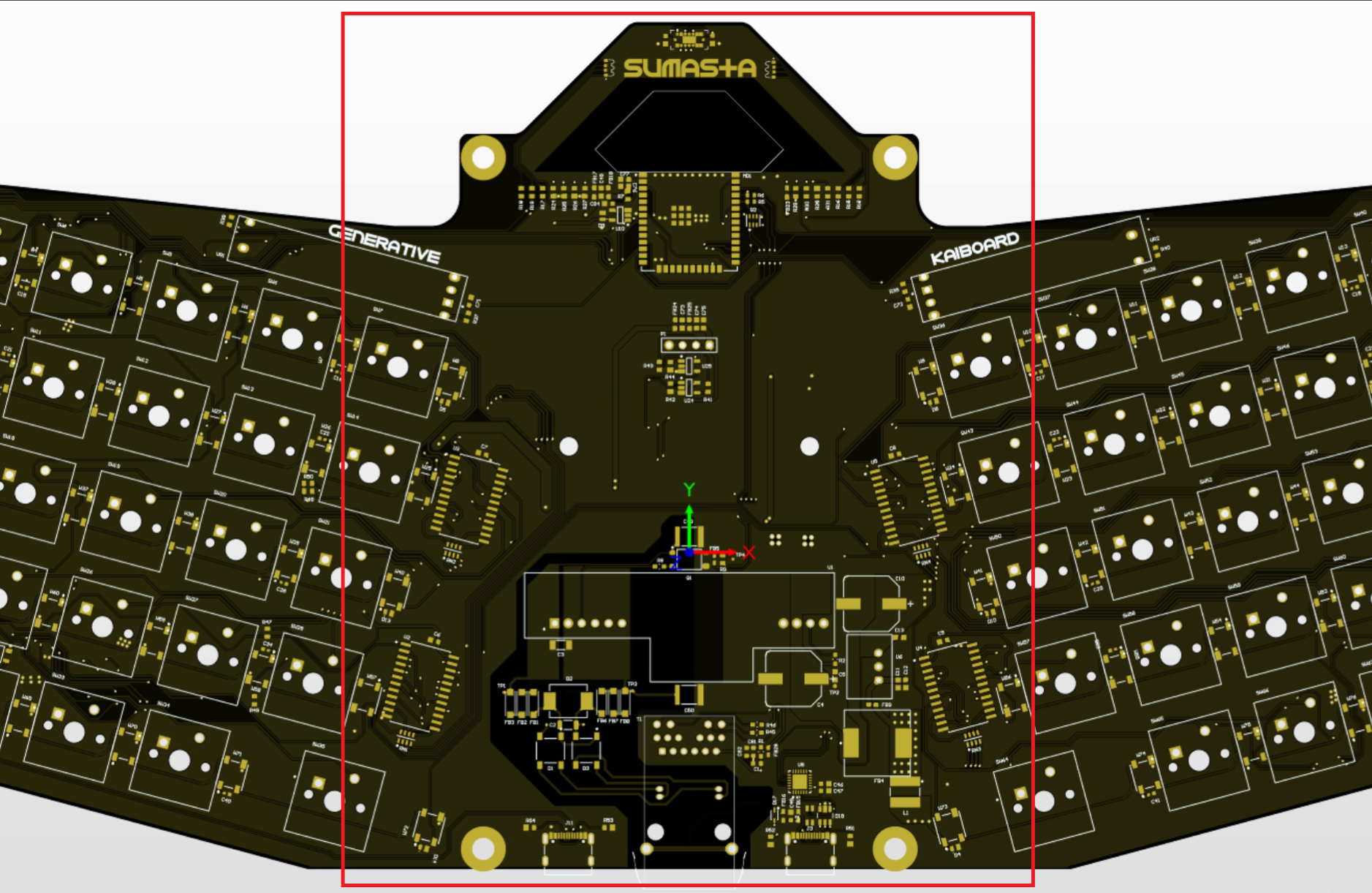
Paste Screening and Reflow (Mid section TOP Part)
As I mentioned in the previous step, in my case I unfortunately had to refrain myself for ordering a large stencil. I decided to crop the stencil only to cover the top mid section of my board while leaving the rest of the board for manual hand soldering. Due to the small area coverage, the screening process also feels easier as you don't have to swipe through a large area. The mid section for screening is approximately as what is shown inside the RED area below.
For this step I assume you have some affinity with handling a manual paste screening process, placing an SMT component manually and have a component reflowed in a reflow oven. So it should be quite straightforward. If you don't have access to Altium Viewer, you can use the assembly pdf files. That way you can easily search where to put each component etc2.
Manual Soldering (Rest of TOP Part)
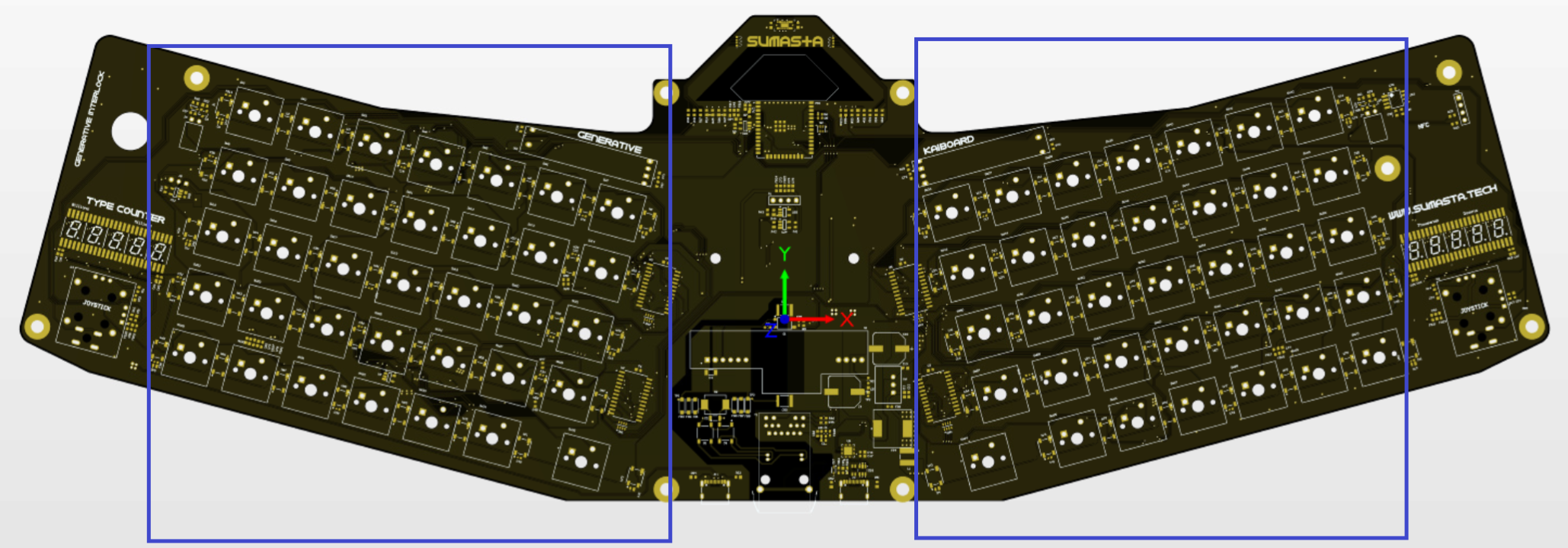
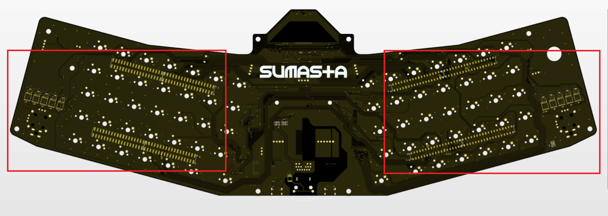
Once you manage to solder the mid section area of the board, you are pretty much has covered more than 50% of the SMT parts. The next big step that I'd highly recommend to do is to solder the LEDs and components located in between the Key-switches. That is mainly because once you've soldered the large key switches, it is quite difficult to reach those parts in between, therefore getting those SMT parts soldered properly and tested is extremely important. So pretty much you have to cover the SMT assembly on the parts in the area marked below inside the blue area.
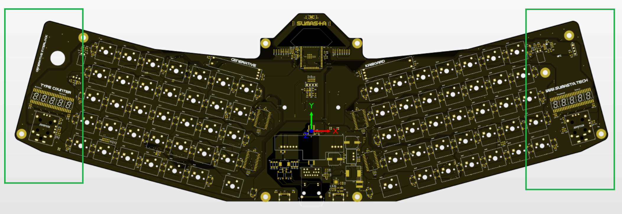
Once you've done that you then follow-up by soldering the SMT parts around the edges of the board. The ones located both on the right and on the left, this mainly covers the 7-segment display as well as few components around. Honestly this is not very critical as you can also do it on the later stage if you prefer. Indicated inside the green area in the preview below.
Manual Soldering (Rest of the BOT Part)
Fortunately there is not much of SMT part you have to solder on the bottom. Primarily are the SMT B2B connectors for the Nucleo board as well as the W5300 TOE shield. Near the side edges of the board however you have to manage some SMT components mainly the shift-registers and some passives. If you've got the right tools and sufficient skills, this should not be very difficult for you. But of course, I can imagine some people will find it quite difficult to solder this, in that case I recommend that you seek help from someone.
Manual Soldering of PSU-related components
Last but not least, once you've completed the SMT parts soldering, I highly recommend that you proceed with soldering few PSU related THT parts such that you can immediately start with sub-system functional test. Those components are:
- PoE Module AG5545 from Silvertel.
- RJ45 Connector MagJack from Wurth.
- SMPS Module 3.3V from Wurth.
All of them are THT parts and should be very easy for you to manage. The parts are highlighted below.
Once you've completed this part you are pretty much ready for initial verification of some board functionalities. I'll detail in the next step. Congrats!
-
5Sub-system Functional Test
Alright, so once you've done the assembly of the SMT parts, I strongly recommend, even insist that you first do some functional verification test before proceeding further. This is important as once you've assembly everything and you just starting to realize that some function are not working, it is going to be much more difficult to debug. In summary I recommend you to follow and do these checks.
- Power Supply / Rails Check
- Co-Processor Programmability and Interface
- WS2812b Check
Three checks I listed above are the bare minimum you have to do prior to proceeding with the next step. Details below.
Power Supply / Rails Check
It is quite obvious isn't it that the first thing to check is the power supply. For those who have worked with PoE design before might find this quite trivial, but for some people perhaps not. First thing first to do is to find a PoE Injector, particularly the ones that is compliant with 802.3AT standard. Watchout for the T at the end there, because that defines the power level of how much the PoE injector can supply. The lowest classification typically states 802.3AF compliant which can supply up to 15W of power. Generally the keyboard will be fine with 15W but you have to put a limit on the WS2812b maximum LED brightness. So if you want to be on the safe side, just get yourself an 802.3AT compliant PoE injector.
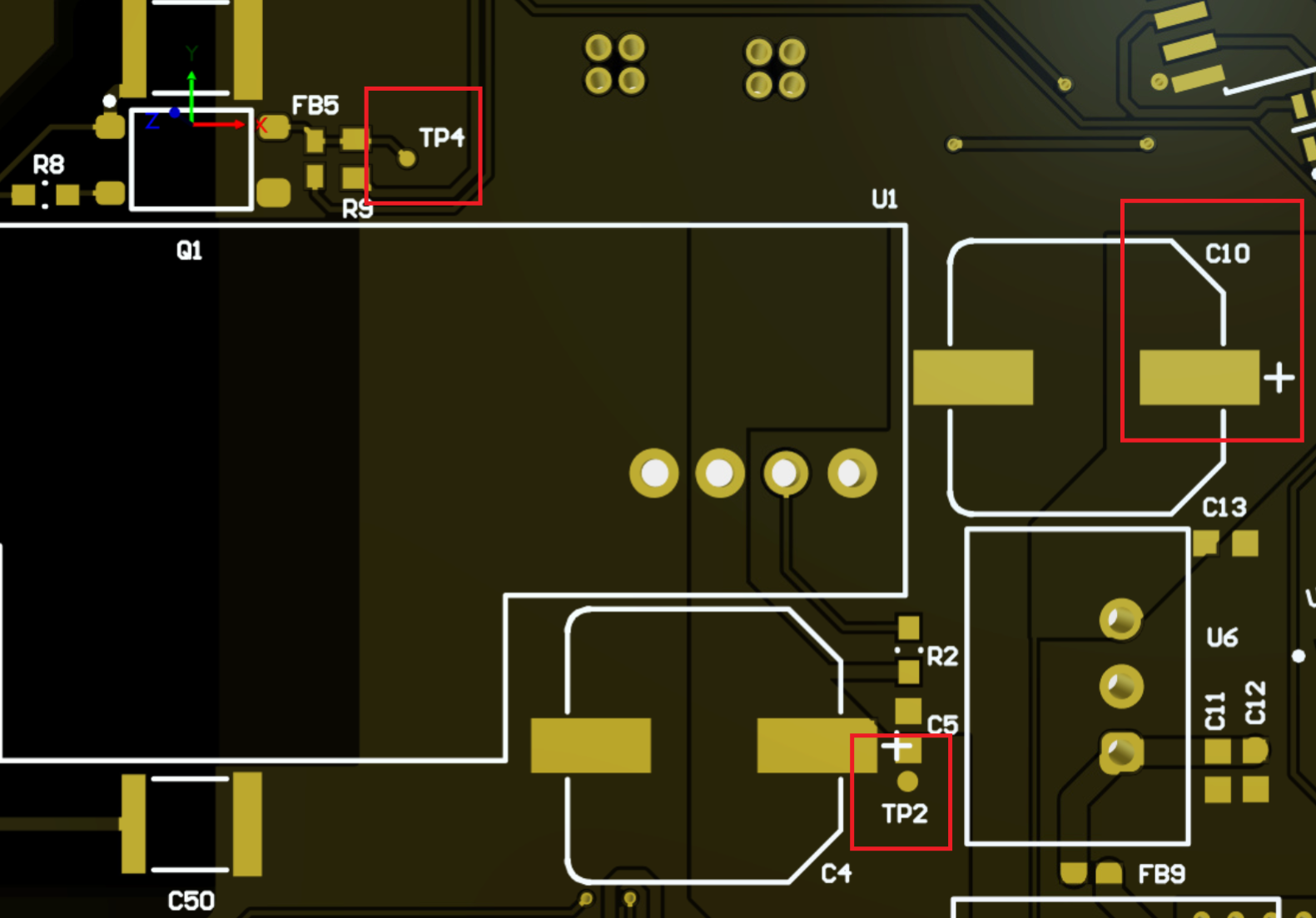
Once you have it in your hand, it should be quite straightforward, you can just plug the output of the PoE injector to the RJ45 jack input on the keyboard. The PoE injector should provide you the power immediately assuming all is ok with the assembly so far. What you need to probe and check are mainly three things:
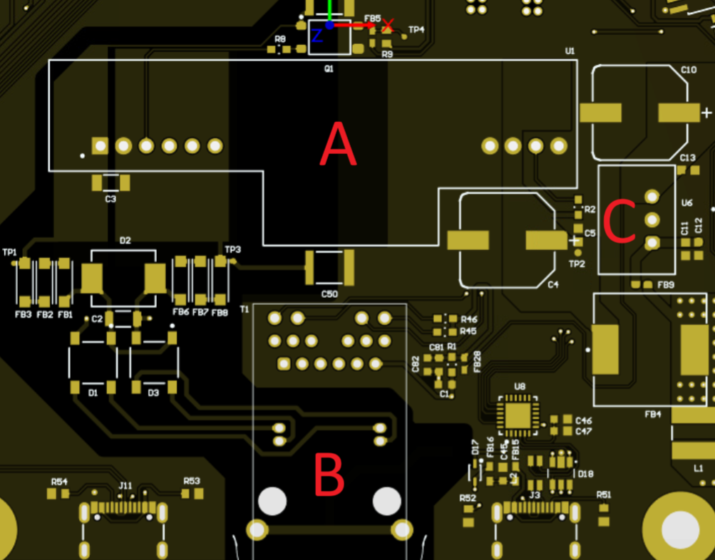
- 5V rails -> output of the PoE module (TP2)
- 3.3V rails -> output of the Wurth SMPS module (C10 + Side)
- AT detect signature -> isolated output of the PoE module GPIO (TP4)
In below picture you can see where to probe those. Measuring the 5V and 3.3V should be straightforward with the multimeter. For the AT detect signature, if an 802.3AT PoE injector has been properly detected, you can expect a 0V on this point. Otherwise if only a 802.3AF PoE injector is detected, this point should show 3.3V.
Co-Processor ESP32 Programming Check
Once you verify the power rails are ok, you can continue with checking whether the ESP32 is programmable and alive. For this step, you'll need a laptop with CP2104 USB-to-Serial driver installed. And I expect also some affinity with programming an ESP32 before. If now please find some tutorial online how to get started with programming an ESP32.
For this test, you'll need a USB-C cable and connect it to one that is on the right side of the RJ45 Jack. This is the one that is connected to the CP2104 USB serial module and ESP32 via a serial interface. First you should be able to detect in your device manager that silicon lab CP2104 is properly detected.
After that you can try to upload dummy code, or even my code for the Co-UC and see whether programming is successful or not. You can configure as though programming just an ordinary ESP32 module etc just for a check. This should be straightforward as well assuming all is ok.
WS2812B LED Check
The next thing I highly recommend to do is to test whether all the WS2812b are working fine. As the principle of this LED is daisy-chain signaling, if one of the LED breaks or not properly soldered, the rest of the chain will not function well or not at all. Prior to continuing with soldering the rest of the PCB, it is important to get it all right, because once you notice some LEDs are broken, you have to de-solder neighboring key-switches first.
Furthermore, for testing the WS2812B you can use generic sample code from FASTLED, or use the sample code of the Co-UC from Github. If you use FASTLED sample code make sure that you use the correct GPIO, set the total number of LED and put some small delay between loop (ESP32 constraint). I recommend you run the Demoreel100 or so from the FastLED Library.
Once you see all LED works and all LED blinks without strange flickering effect, that means you are ready to proceed further!
-
6Assembly PCB THT Parts and Internal Wirings
Well done, if you've successfully reached this part. You are almost there! There are just few more soldering steps left. In short here are the few more things you have to manage:
- Solder the key-switches.
- Solder the Joysticks
- Mount and solder the Interlock Switch and THT Connectors
- Solder the internal wires (Ethernet and USB)
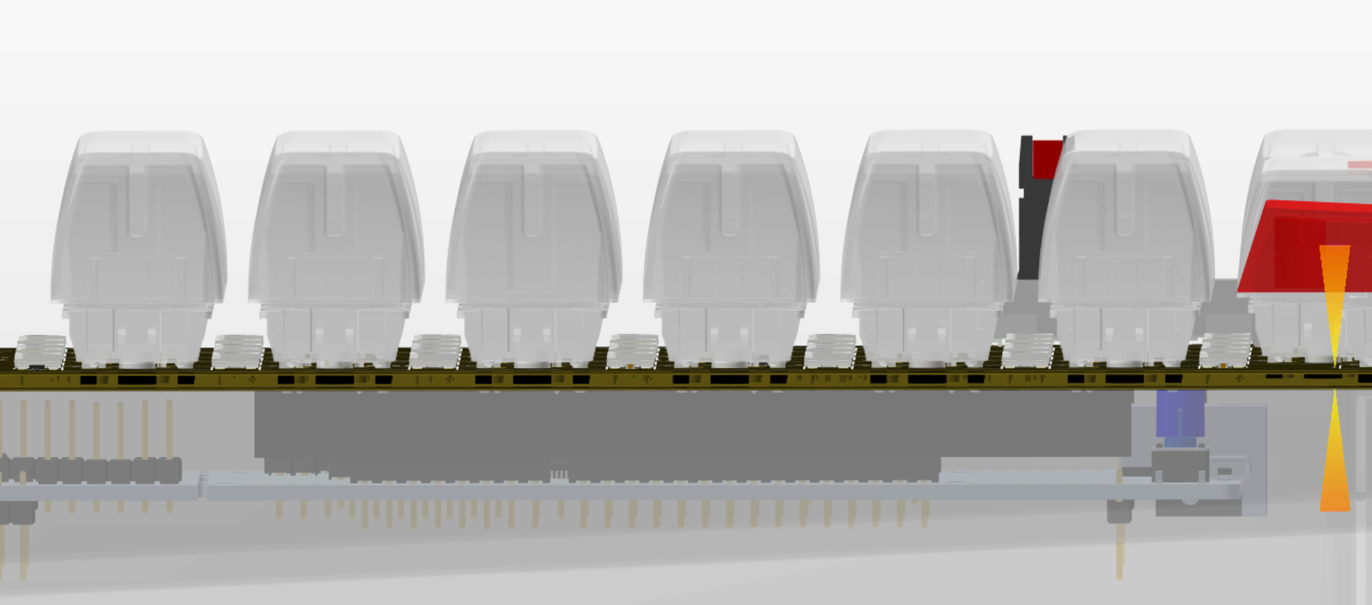
- Install the Light strip on the side (Optional)
Solder the key-switches
Once you fully confirmed that LED fully works and all the SMT components around the key-switches area are soldered, you can then proceed by soldering all 70 of the key-switches. It should be straight forward and easy. What you need to watchout is that if you order for instance the Cherry MX without the additional 2 extra alignment pins, you have to be extremely careful in aligning it during soldering. because it is very easy to misaligned and the holes on the PCBs are not tight-fit. So what I'd do is that you solder first on only one pad, once it is mounted, then you heat-up that one-pad, realign the key-switch and then once it is straight, you start soldering the 2nd pad making it stuck in place. So take care on the part number of the key-switches whether that has alignment pin or not.
Solder the Joysticks
There are Two joystick on each bottom corner of the board. You can simply solder it and make sure that all the pins are flushed inside, and the bottom surface of the joystick touch the PCB completely. Because if you do not place it right the first time, de-soldering or reinserting it is going to take some force.
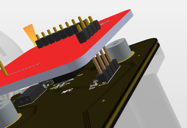
Mount and solder the Interlock switch and THT Connectors
On the left side of the keyboard, as you can see I have a physical switch which is labelled generative interlock. You can mount it through the 12mm hole and solder the 2 pins on to the appropriate connector. It should be straightforward as well, but you need take care about the height of your switch, in my case I had to bend the bottom pins as it is protruding too much.
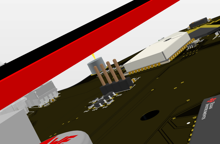
On top of that there are also 2 THT connectors you might have to manage, that is the UART connection connector for communication with Nextion LCD and on top of that the I2C connector for a connection to the NFC module. They are located as shown below:
Well on top of that there are actually two vibration motors that you need to solder as well one on each side.
Solder the Internal Wires
In general there are three internal wires you have to manage, the ST-Link USB programming wire, the Ethernet wires and the Ethernet LED-state wire. The Ethernet LED-state wire is however optional, only if you want to see the Ethernet link activity from the outside through the built-in LED in the Magjack RJ45 connector.
So first thing first is the ST-LINK USB wires that you have to manage. the main purpose of this wiring is to enable programming externally via one of the USB-C, the one located on the left side of the PoE injector. In theory you don't really need this if you are not planning to make modification to the SW of the main controller, the STM32. You can just program it once prior to closing the back housing. I anyway recommend you to do it as it is going to ease your life if you decide to make adjustment along the way.
There are essentially three wires to manage here, the 5V_USB, D+ and D- of the USB. you can in the picture for the connection diagram.
If it's soldered well, you should be able to detect the STLINK via the external USB-C connector.
The next internal wiring to manage is the Ethernet MDI interface. There are essentially 4-pins which consists of 2 x differential TX and RX pins from the PoE Mag-jack to the W5300-Shield. This connection is essentially bypassing the connection from RJ45 Magjack on the Generative kAiboard PCB on to the W5300 shield. What you need to do first is actually to unmount the RJ45 jack on the W5300 Shield. that is mainly due to the mechanical height constraint. If you have the RJ45 connector on the W5300 shield, you will likely have some mechanical clearance issue in the back housing, unless you design a taller housing yourself.
So on the connection-wise you should connect the 4 wires as per below directly from the pin of the Magjack connector on the Generative kAiboard PCB onto the W5300 Shield.
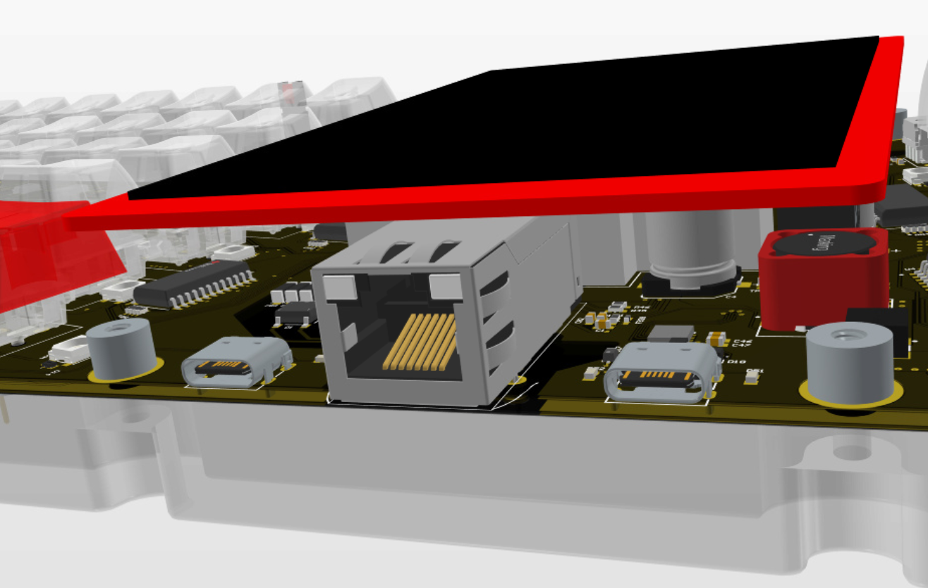
Lastly to enable the LED indicators on the RJ45 Magjack, you can solder the 4 wires directly from the W5300 shield to the LED pins of the Magjack as per diagram below.
Light-strip installation and soldering
I have to say, having a side emitting light-strip was not part of the original plan. My plan was actually to have a flexible filament, single color mounted on the side. But that turns out to be more tricky as I have to manage an external LED driver, PWM control etc etc, so in the end I decided just to add a WS2812 Light-strip that can directly accept 5V and I can feed identical signal as for the WS2812 on the top side.
So this is pretty much an improvisation and you can also do what you want here. In my case I had to use a glue gun, nylon nuts etc to hold the light-strip in place. You can choose here. What's important is to tap the 5V, GND and data connection from the PCB.
-
7Full-system Functional Test
At last, once you sure everything have been assembled, you can then do final complete functional test prior to doing complete final assembly. In summary, the complete the HW functional tests should more less verify each of the part listed below. It is also primarily split into two categories depending on whether that section is connected directly to the main ucontroller STM32 or the co-processor ESP32.
STM32 Main Controller:
- Ethernet Connectivity with W5300 Shield
- Key-Switches and the Multiplexer
- UART Connection to the LCD
- UART Connection to the ESP32
- I2C ToF Sensor
- I2C PN532 NFC
- I2C EEPROM
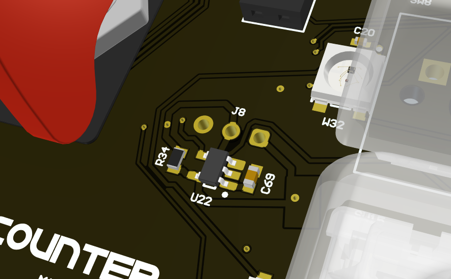
- 7-Segment Display Keycounter
- GPIO GPT Interlock Switch
- Vibration Motor
ESP32 Co-Controller:
- BLE Connection
- Joystick Analog input
- Slider Analog Input
My intention is to provide you with the example test code in which you can run the program and it basically checks each one of the part subsequently. I'll post the code on my Github once it is ready.
-
8Final Full Assembly
At the very end, once you have confirmed that every single part of the board works, you can then do the final assembly which mainly should consist of:
- Assembling the back-housing
- Mount the LCD, connect the wiring and install the speaker.
- Install the keycaps
- Install the joystick keycaps
- Install the NFC tag reader
-
9Follow-up Resources
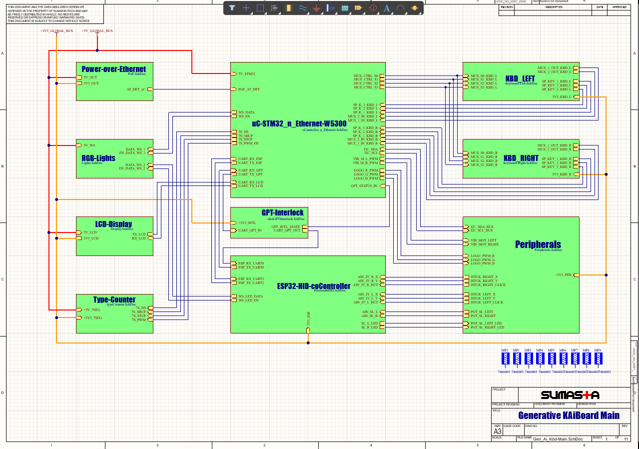
Should you have still some questions, especially in the electrical connections and wiring, best thing to do is to deep dive the schematic. I exported the pdf version of it of course, and below you can see what each of the sheets contains. The Schematic is designed in a hierarchical way, it should be pretty easy to understand if you have never worked with it before.
![]()
So In summary:
- Power-Over-Ethernet Sheet: It's all about safety and power. Shows you how the PoE circuitry works and how it connects to the W5300 shield. Basically, it's your go-to guide for understanding power distribution and Ethernet controller integration.
- STM32 & W5300 Sheet: This one's like the keyboard's wiring map. It spells out how the STM32 and W5300 connect to each other and to the stuff around the keyboard. Think of it as the blueprint for how everything talks to each other to make the keyboard work.
- RGB Lights Sheet: Want to know how those fancy RGB lights are hooked up? This sheet's got you covered. It explains the serial connection setup for the WS2812 RGB LED lights, so you can see how the magic happens.
- Display Sheet: Shows how the STM32 controller connects to the display controller. It's like the visual link between the brain and what you see on the screen.
- Type-Counter Sheet: Ever wonder how that 10-digit 7-segment display works? This sheet breaks it all down, from the connections to the power setup. It's your guide to understanding how the numbers show up on the display.
- ESP32 HID Controller Sheet: Dive into the co-processor's world. This sheet spills the beans on how it works, what it controls, and how it's programmed through USB-C. It's your comprehensive guide to the co-processor's inner workings.
- GPT-Interlock Sheet: Simple switch stuff to keep things secure. It's all about preventing remote shenanigans.
- Peripheral Sheet: Covers all the extra hardware, from joysticks to Time-of-Flight sensors. These sheets show you how they connect and bridge the gap between the main processor and the co-processor.
- KBD Sheets: Get down to the nitty-gritty of those Cherry MX switches. See how they talk to the main processor, and how the signal flow is optimized for quick and accurate typing. It's the secret sauce behind the keyboard's responsiveness.
-
10Still stuck?
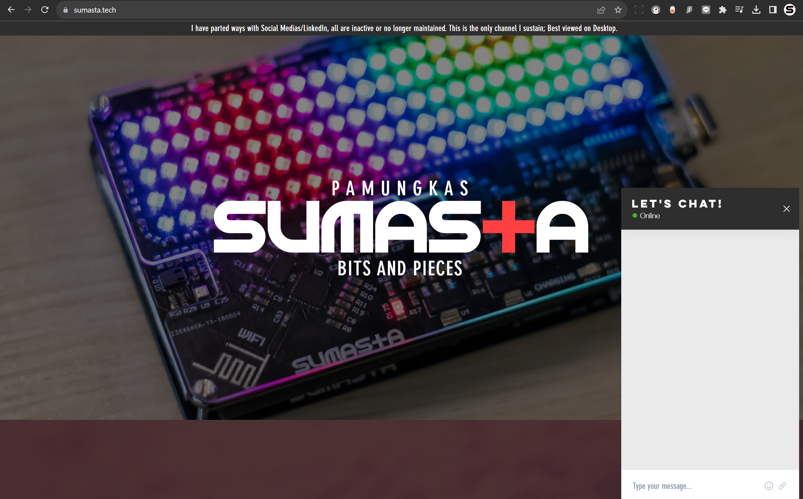
Well if you're still stuck and in need of urgent help, feel free to reach me out directly at my personal website www.sumasta.tech and go to the chat column on the bottom right corner. This goes to my phone directly 24/7 :)
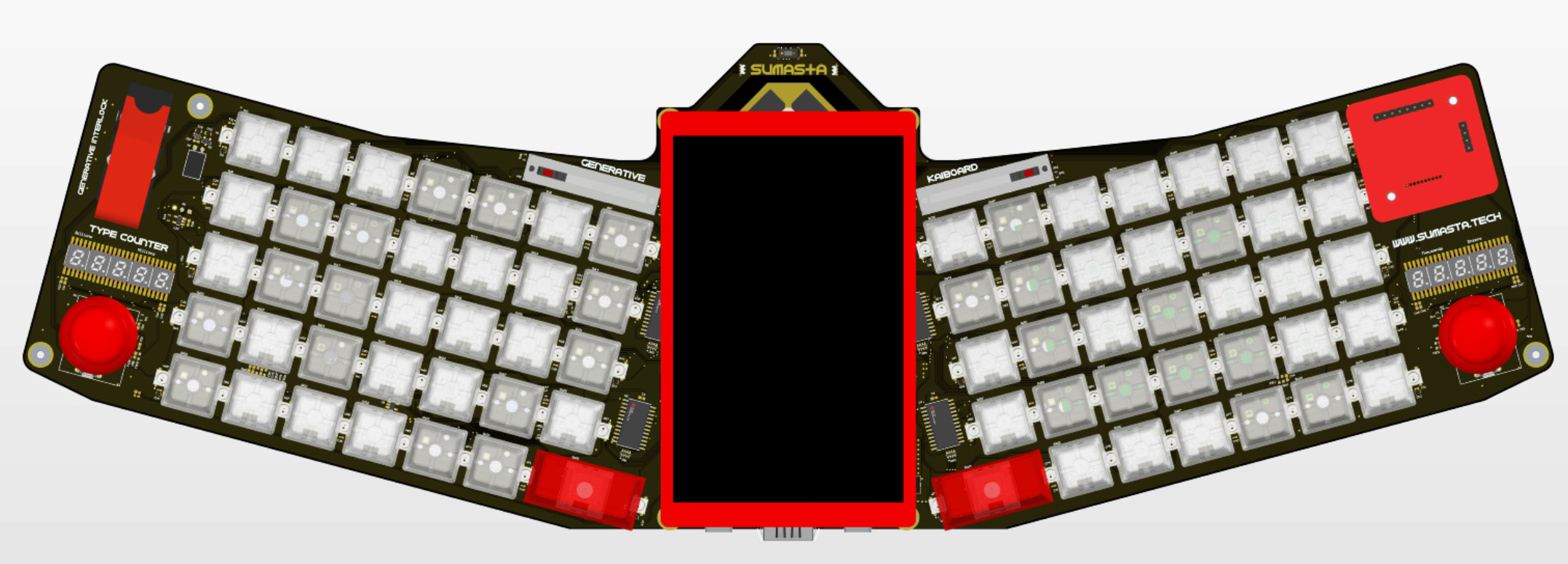
Generative kAiboard
Beyond Typing: An Adaptive Hardware Prompter for the Age of Generative-AI. Internet-connected. Built-in ChatGPT.
Discussions
Become a Hackaday.io Member
Create an account to leave a comment. Already have an account? Log In.