Nyan Keys - Hardware
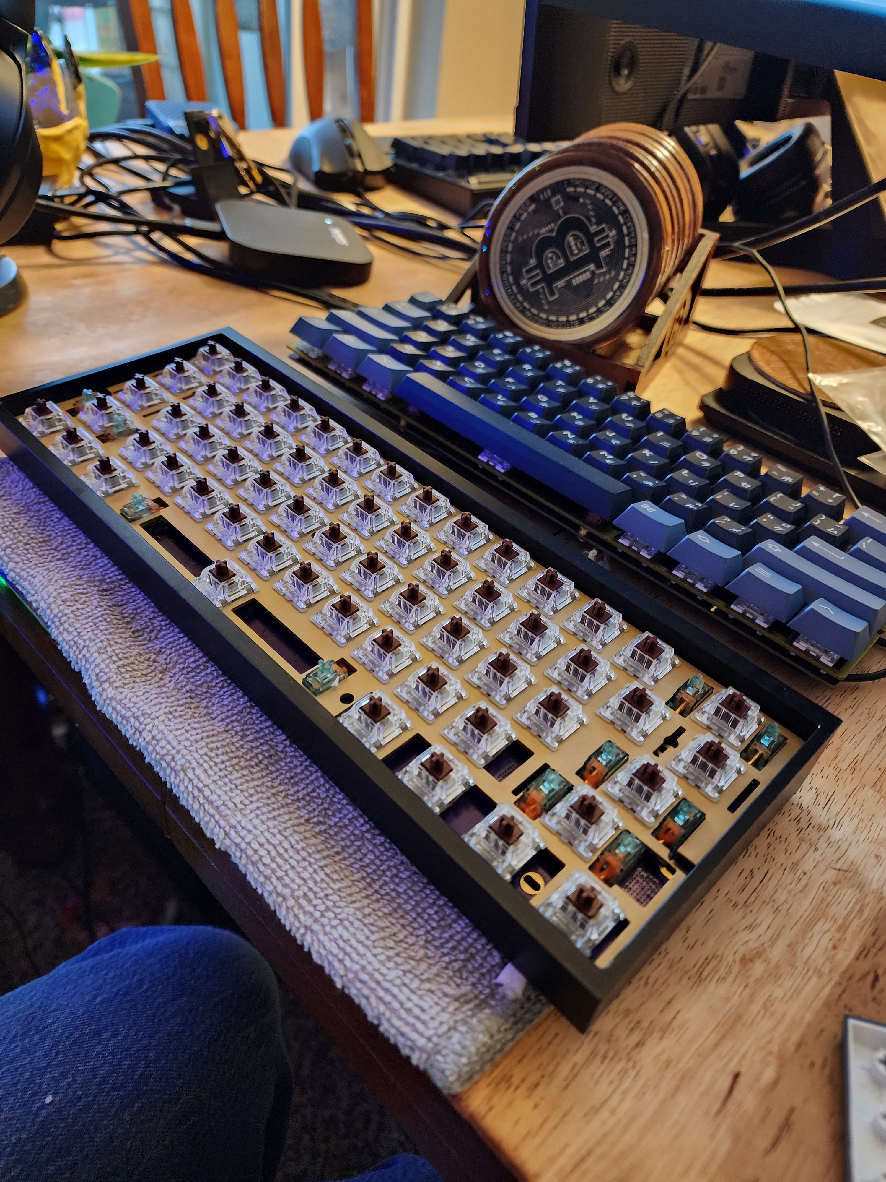
The purpose of Nyan Keys was to engineer the lowest possible latency mechanical keyboard that would accept any Cherry compatible switches, e.x. Kailh and Gateron.
The hardware inspiration came from the Wooting 60HE and Pok3r 60% mechanical keyboards. Where the performance characteristics of the Wooting were desired but with the freedom to use any off the shelf switches of the Pok3r
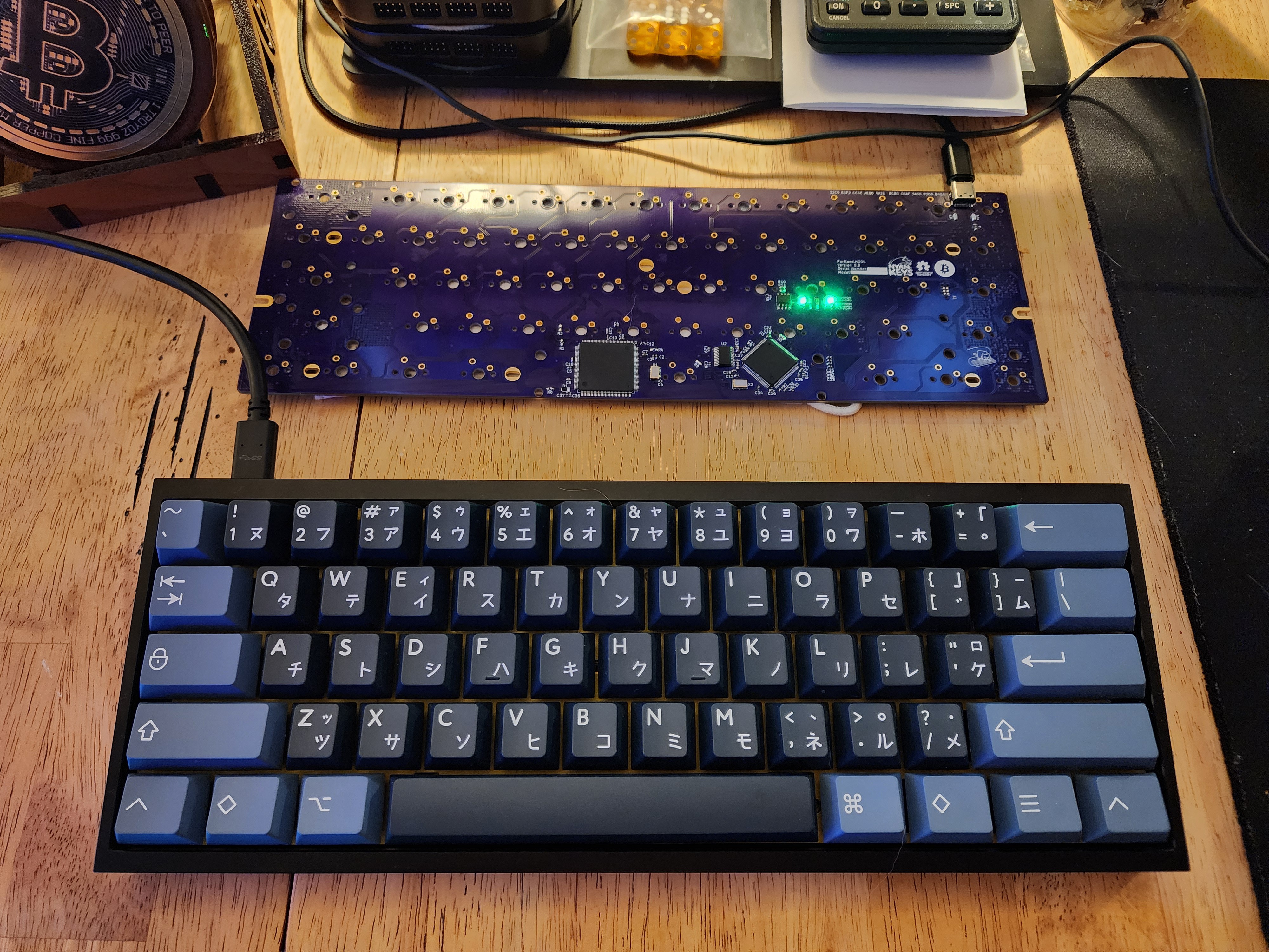
Latency 🚀 (The Numbers)
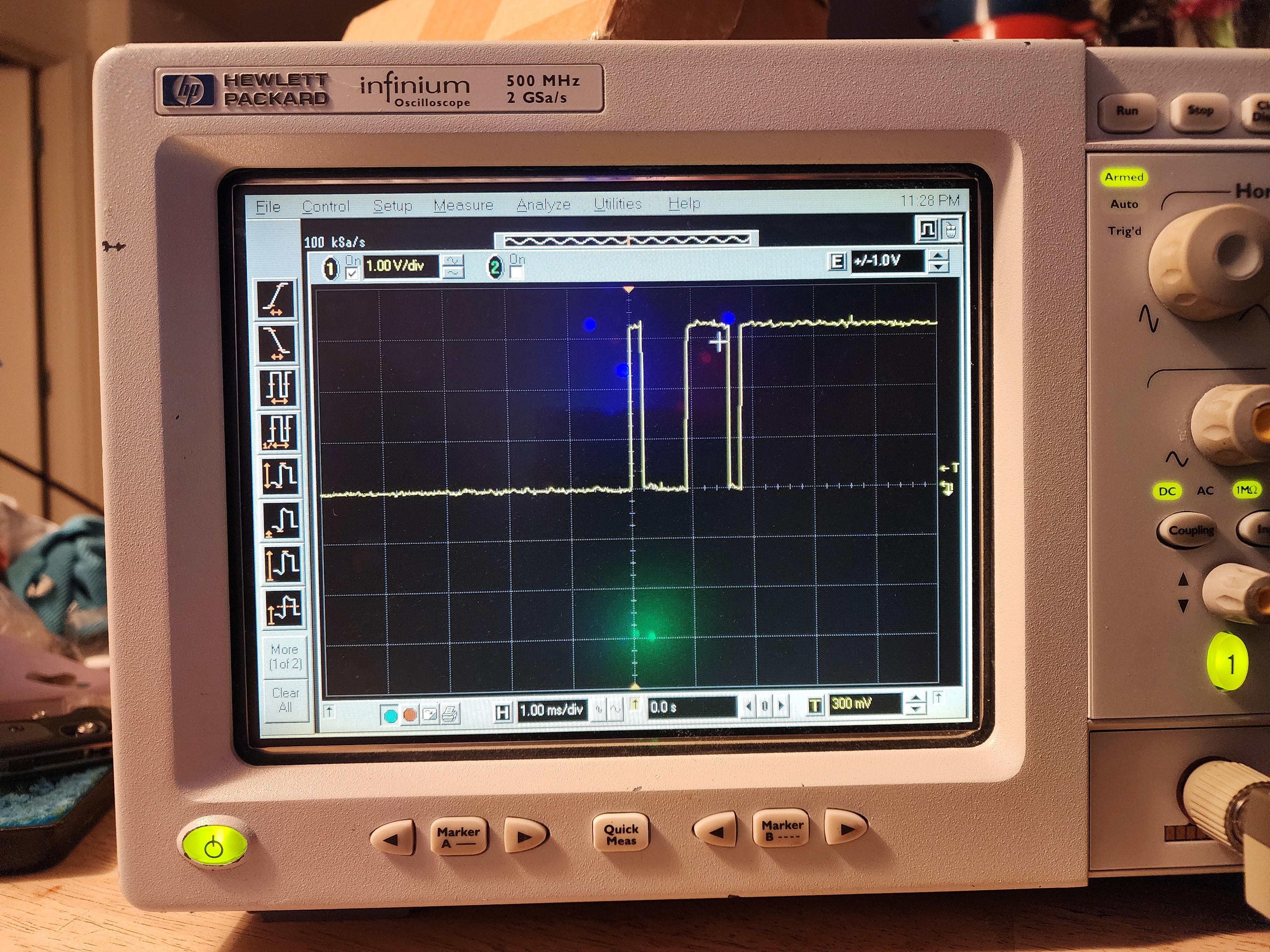
Nyan keys is fast... really fast. Key latency is unmatched at 30µs worst case while the SPI bus between the FPGA and the MCU is running at 12.25Mhz.

The above is a simple test of when the switch logic level goes low how long until the 'USB Frame Transfer Time' line goes from low->high->low. This is the total time between keypress and the the buffer for the next usb interrupt to be set. This is not the end all be all though. the host still has to interrupt the keyboard at 8000hz to get that data that was just set from from the key press. The bInterval of Nyan Keys is set to 1 at USB2.0 HS, which means 8000hz or .125ms. Lets us assume the worst case scenario where the key is pressed right after the last frame was requested and sent to the host. We would take out 30us latency then add that to the 125us latency of the USB Interrupt transfer to get ~155us. This is 6.5x faster than any usb 2.0 FS based keyboard (The current market) which have an interrupt rate of 1ms and you have to also add in the latency of scanning the matrix. giving Nyan Keys not just the win in the most over engineered solution to a problem that .00001% of people would have, but likely the lowest latency solution available.
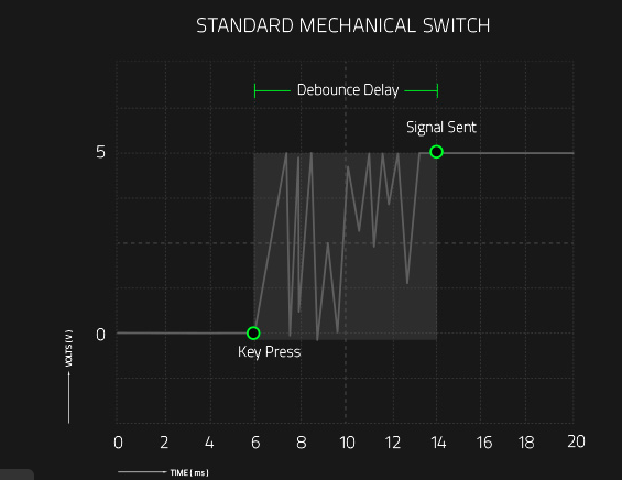
Notice how the switch state is sent before the the switch is even done bouncing. This is because you can arm the debounce counter to prevent a state change after the initial press or release of the key.
FPGA
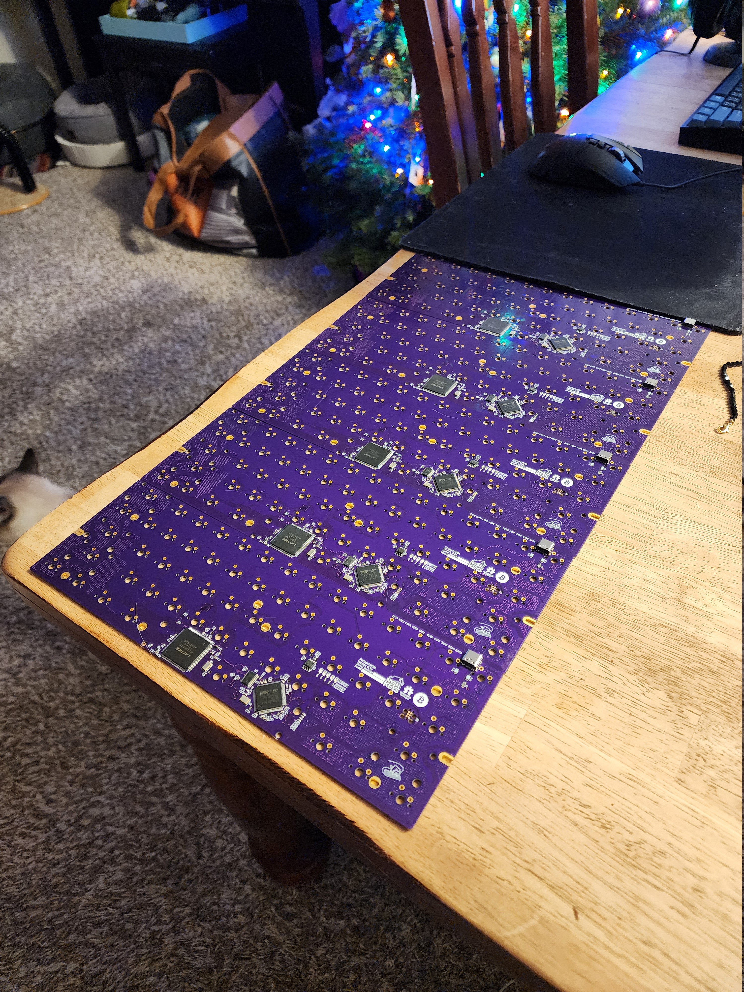
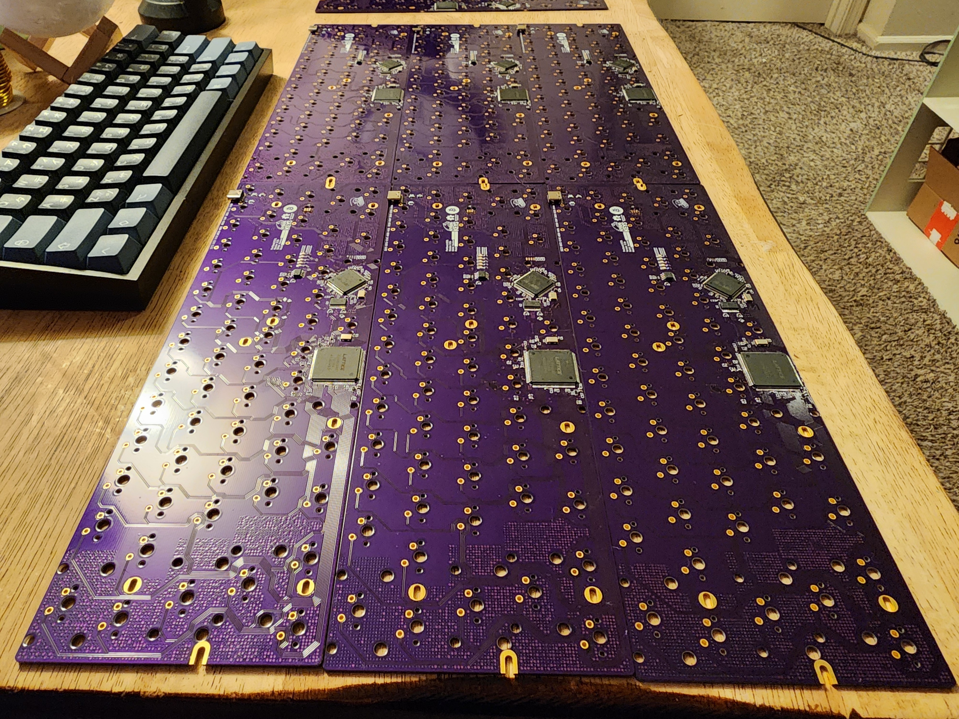
The most novel element to Nyan Keys is the use of an FPGA to handle the debouncing logic and serialization of the parallel keys interface. Using an FPGA had the advantage of being able to wire each switch to it's own IO pin, which could be pulled high with the internal pull-up resistors on the Lattice Ice20HX4K IO block. This design greatly increased the routing complexity but at the same time removed any need for additional components such as diodes with each switch.
Using and FPGA allowed for the ability to give each key (switch) it's own core, which consists of an 8 bit timer. The timer is always counting up to the value of 255, once the counter reaches the comparison value the key can change its state and the timer will reset to 0. While the counter is any value that is not 255 the switch state can not be changed. This is the debounce mechanism.
There are 2 primary advantages of the above method for debouncing. The first is that the key press is able to be instantly registered for the press and release as long as the debounce lockout counter has passed. Second it's very area efficient using ~25-30% of an Ice40HX4K for 61 total keys.
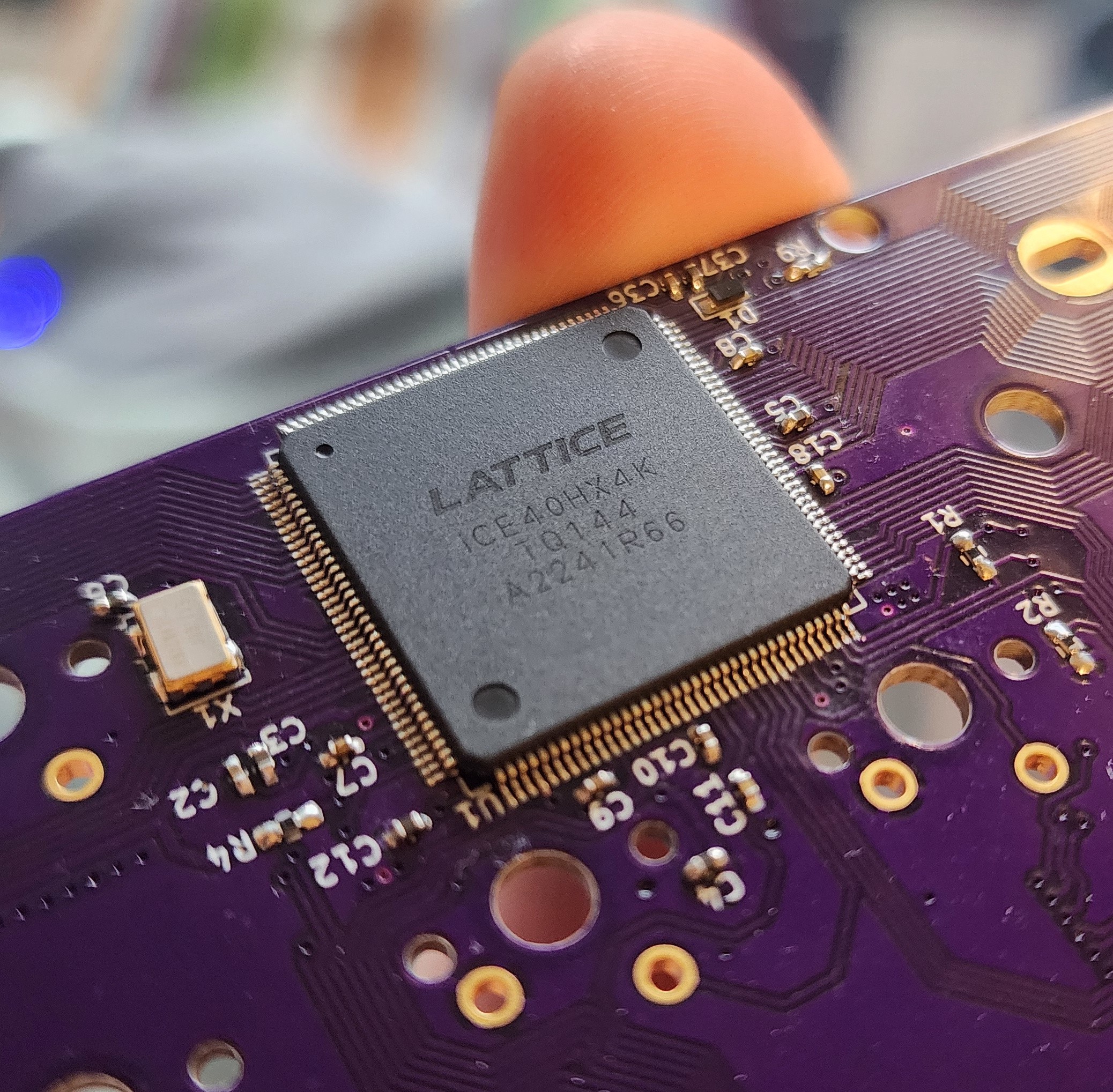
Some of the initial designs were very area inefficient and as such would use a majority of the PLBs of the lattice ICE40 FPGA. This led to the initial versions which had an up AND down counter for the debounce to use more than the available logic blocks on an ICE40HX1K IC. This design was safer from electrical noise and very accidental touches but increased the latency by the time of the counter to even get the switch to change state.
The new revision scrapped all of that an instead just uses an UP counter as such the new logic just uses NUM_KEYS * COUNTER_REG_WIDTH registers and the total area used was reduced by nearly 75% given the same width debounce counters. This can be seen below in the .PNG showing the various elements of the PLB that are used once the verilog is synthesized and routed. This new approach also removed the need to synthesize subtractors and replaced it with much simpler...
 Portland.HODL




 Guy Dupont
 deʃhipu
 Pamungkas Sumasta
I would love to pick one of these up for a build, I sent you a pm and would be great to organise a way to buy it from you