WSX.COM (Portable WordStar driver for the PX-8 version 2.3)
The Filink file set of the V7.11c are:
IRM.COM Integrated Resource Manager version 2.7 for the PX-8)
PIN-DRV.COM (UD-80++ driver version 1.8p)
WSX.COM (Portable WordStar driver for the PX-8 version 3.1)
This suggests V5.21E is intendend for the PX-8 and V7.11c is for the PX-4. The two WSX.COM files are different, which is then expected. But the IRM.COM will not run on a PX-4, as it complains it needs a newer OS-ROM, M25030CB. But this ROM is for the PX-8, not the PX-4. The IRM.COM needs 25 pages of User-BIOS. Text in the file refers to the DS-8.
AFAIK, there is no Portable WordStar for the PX-4. The internal version numbers are different, so both are mostlikely for the PX-8.
The PIN-DRV.COM seems to execute without error on the PX-4 (assuming 4 User-BIOS pages), but does not reroute the console to the UD-80. 'Pine' is the internal name for the PX-4 board. The PX-8 is 'Maple'.
(The 7.11c version is a patch from the original 7.11A, so it works with the Re-UD-80. Otherwise they are identical. the bytes changed are the EF9345 register setting, the banner text and the checksum)
After testing and undoing the sync modification for the 7.11A firmware, one board stopped working (no video output). Comparing some scope signals with a working board the problem was found; a not working 74HCT04 produced a distorted clock for the EF9345. Replacing it with a 74LS04 fixed the issue.
The 74HCT04 was tested with my TTL-tester, and functionally it works OK. Apparantly it doesn't want to work with the 12 MHz crystal! It might have oscillating at 24 MHz, but with other signals interfering.
Below the video signal at the base of the Q1 transistor.
The board is prepared for the classic 9V DC wall-brick, supplied through a barrel-jack 2.1/5.5mm with pin positive. The regulator has the same pin-out as the LM7805. There is little room for a cooling sink, so a switching regulator is advised. On the other hand, power consumption is modest, ~200mA, so it is feasible to power the board directly from a USB charger or power bank. Do not solder a 7805 and short its input solder pad to the output pad and directly connect 5V to the barrel-jack socket. This works quite well. I have yet to add a regulator to a board.
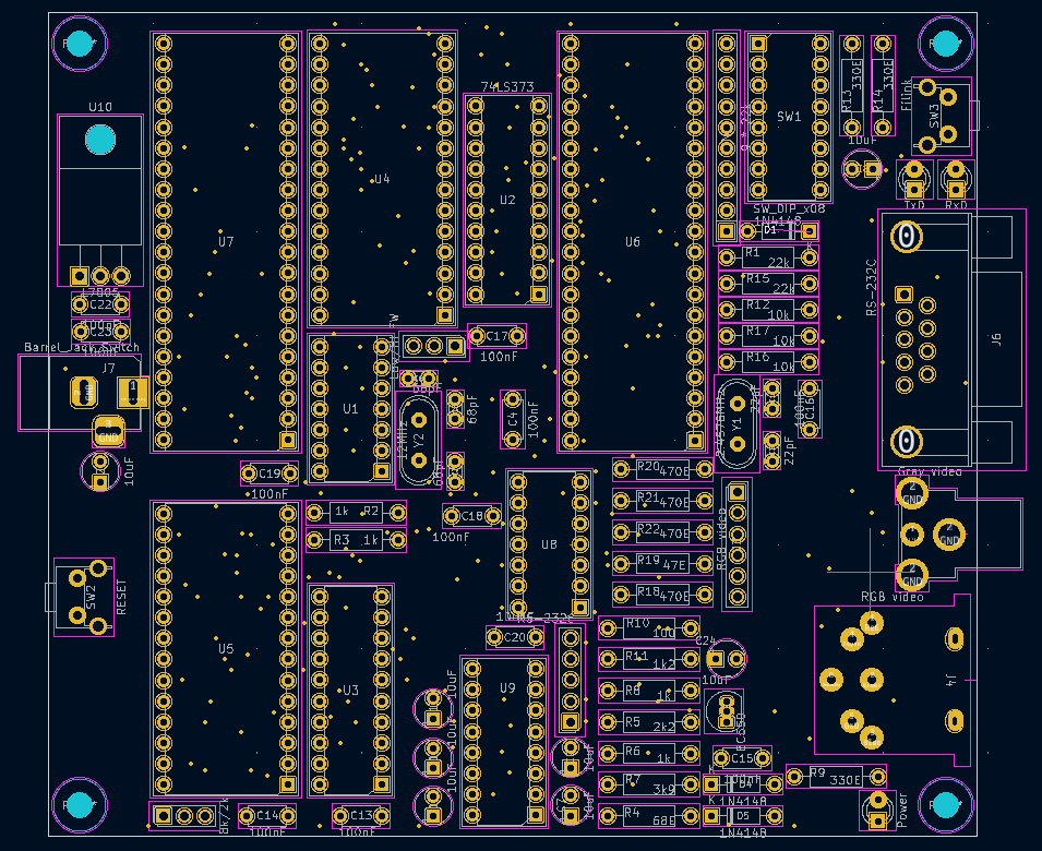
Connectors
See the oval80replicaV0.10.connectors.pdf file (files section) for more info on what connector or jumper should do.
List of unstructured information and observations:
The Re-UD-80 can use both 2k and 8k Byte Static RAM, as this was a jumper option for the UD-80. I am not sure the extra 6 k Byte is actually used. This is jumper J1 on the replica.
The Re-UD-80 can accommodate 27128 and 27256 EPROMs, or the CMOS versions of those. The address range remains 16 kByte, but a larger 27256 can be used to switch between two firmware versions. This is jumper J8.
The RGB video DIN-part is used for color displays. The RCA plug carries a gray-level signal. I have yet to see an indication that color is actually used. Other color-only components: R18 to R22 and C24.
The ROM is in the upper half of the memory space of the 6803, it uses it's internal RAM for housekeeping. The RAM is only accessible by the EF9345. The eight registers of the EF9345 fill most of the lower half of 6803 memory (excluding space reserved for internal RAM and registers).
When the ROM isn't seen by the 6803, the serial LEDs can blink rhythmically. During normal operations they are off. One blink when the Filink switch is pressed, and more during Filink transfer and normal access.
When the RAM isn't seen by the EF9345, a video signal is generated, but filled with random characters.
The R, G and B channels for the gray-level output have different series resistors, which should allow for eight different gray-levels.
The 74LS08 can be replaced by a 74LS32. Not because AND is the same as OR, but all the gates are used as buffers, and the pinout is the same.
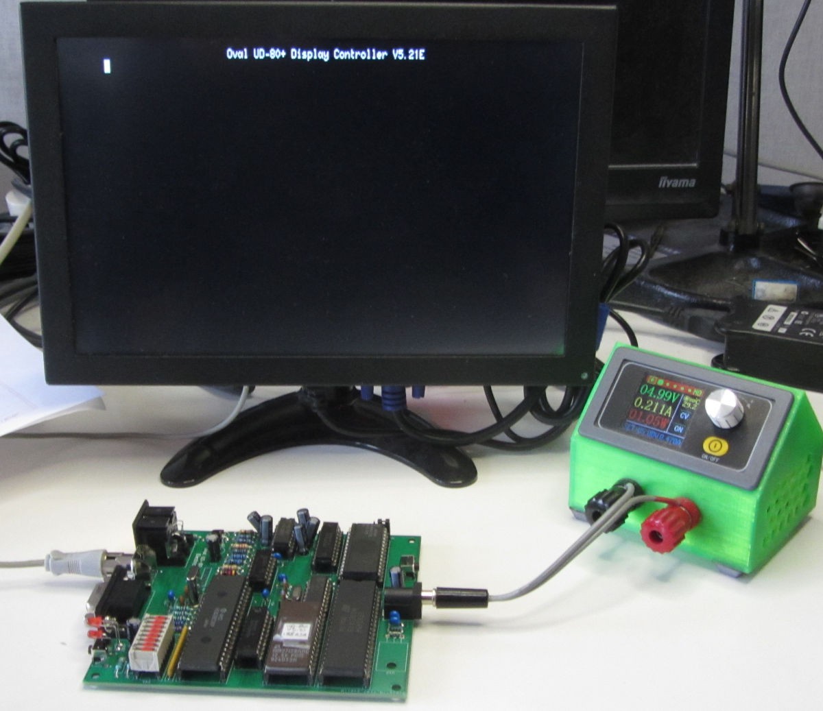
The top line of the screen is reserved by the banner: Oval UD-80+ Display Controller V5.21E
or Oval UD-80A++ Video Controller V7.11c
When you want to test the Re-UD-80 without having the cable to the PX-8 or PX-4, you can connect it to a PC and send characters to the serial to which it is connected; 4800Bd, 8 bits, no parity.
When you cannot find a cheap MC6803 or HD6303, an MC6801 will also work. The 6803 is a limited mode version of the 6801, but capable of the mode used in the Re-UD-80.
As previously reported, the 7.11A ROM didn't work properly with the Re-UD-80 because of the video sync signal configuration. The 5.21E ROM used one pin for both horizontal and vertical sync, the 7.11A ROM used two pins. The board can be modified to work with the 7.11A ROM, but not without loosing5.21E compatibility. Adding a jumper would mean a new board version. Instead I attempted to change the configuration of the EF9345 video controller in the 7.11 ROM to match that of the 5.21E ROM. This was successful, resulting in the 7.11c ROM. The ROM image can be found in the Files section: ud80_rom7.11composite.zip.
In total four bytes are different between the 7.11A and 7.11c version; the TGS configuration byte, one character of the permanent banner and the two checksum bytes.
With this result, I think the project is completed. It might be interesting to explore the features of the UD-80, but that has to compete with other planned projects.
The 5.21E ROM works file with the current board, but the 7.11A ROM uses a different pin for the vertical sync signal. This can be fixed, but then the 5.21E ROM results in no display. Rather than fixing the hardware (with a jumper to be changed when the ROM is changed), an attempt to patch the 7.11A ROM is attempted first. And as a first step, the 5.21E ROM is disassembled. It is smaller, only 8 kByte large, of which 3.6 kByte are the drivers.
One part of the problem is finding the configuration of the TGS Register in the EF9345 where the sync configuration is set.
Another problem is the ROM checksum. This is the part calculating the checksum:
; summate all bytes $8000-$9FFF into B
Z8D3C CLRA ;8D3C: 4F 'O' ; A zerooed
CLRB ;8D3D: 5F '_' ; B zeroed
LDX #M8000 ;8D3E: CE 80 00 '...' ; ROM start address
LOOP ADDB ,X ;8D41: EB 00'..' ; [X] + B -> B
ADCA #$00 ;8D43: 89 00 '..' ; A + [$00] + C -> A
INX ;8D45: 08 '.' ; I++
CPX #MA000 ;8D46: 8C A0 00 '...' ; ROM end address + 1
BNE LOOP ;8D49: 26 F6 '&.' ; loop
LDX #M9FFC ;8D4B: CE 9F FC '...' ; [9FFC] -> X ; NMI handler ? (43 F5)
SUBB ,X ;8D4E: E000'..' ; B - [X] -> B
SBCA #$00 ;8D50: 82 00 '..' ; A - [$00] - C -> A
SUBB $01,X ;8D52: E001'..' ; B - [[$01]+X] -> B
SBCA #$00 ;8D54: 82 00 '..' ; A - [$00] - C -> A
SUBD ,X ;8D56: A3 00'..' ; D - M:M + 1 -> D
BEQ CHKOK ;8D58: 2706''.' ; branch when Checksum is ok
LDX #Z8FB6 ;8D5A: CE 8F B6 '...' ; load Checksum error message pointer
JSR PRTMSG ;8D5D: BD 8C 2F '../' ; print 0 terminated message on screen
The sum over the original 8kByte ROM is 0x0C452D.
When the 0x9FFC and 0x9FFD bytes are zeroed, the sum value of the ROM (0x8000 - 0x9FF) is 0x43F5. This matches the original values at 0x8000 - 0x9FF.
Reversing this for a patched ROM:
set 0x9FFC and 0x9FFD bytes to zero,
add all byte values,
insert the lowest two bytes in 0x9FFC and 0x9FFD.
The crude perl program for getting the checksum (which matches that of the Eprom programmer):
#!/usr/bin/perluse strict;
my $byte;
my $byteStr;
my $address = 0;
my $sum = 0;
my $count = 0;
if ($ARGV[0] eq '') { die"Usage: perl binsum.pl <file.bin>"}
open BFH, "<$ARGV[0]"ordie"binsum.pl cannot open file \'$ARGV[0]\'";;
binmode BFH;
while ( read BFH, $byte, 1 ) {
my $byteVal = unpack("W", $byte);
$sum = $sum + $byteVal;
$count++;
# print (sprintf("%06X", $sum) . "+" . $byteVal . " ");
}
close BFH;
print ("Count: ");
print (sprintf("0x%0X", $count) . "\n");
print ("Sum: ");
print (sprintf("0x%06X", $sum) . "\n");
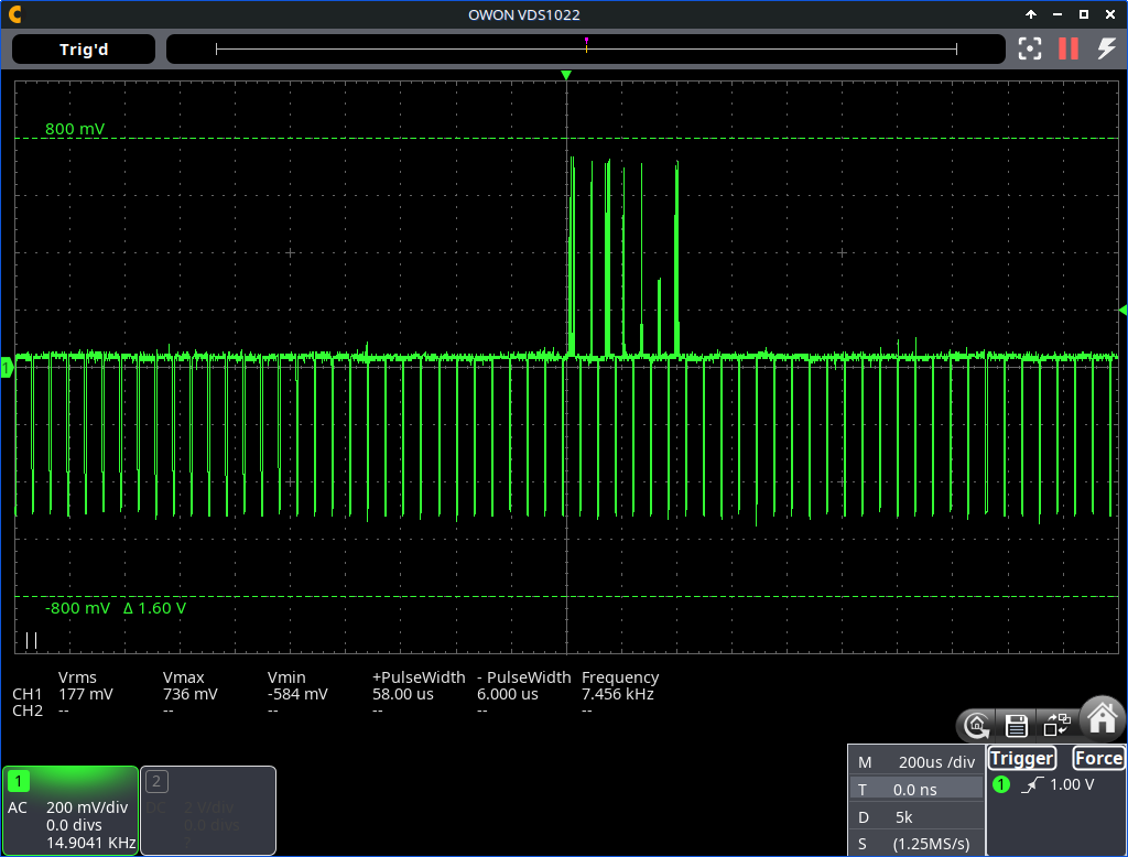
Initial testing was done with the 5.21 firmware, which has the PX-8 driver programs. This firmware uses the EF9345 Display Processor pin 5 (HVS/HS) for the sync signal. When the 7.11 firmware was used for testing, the vertical sync was missing, resulting in a vertical rolling of the screen. The scope confirmed that the vertical sync is present on pin 6 (PC/VS). This led to the fix described below, which ANDs the two signals to a combined sync. But then the 5.21 stopped producing a screen, as pin 6 is low continuously.
The fix for 7.11 broke the 5.21 firmware. Looking at photo's of the original board, it seems pin 6 is not connected at all to the video circuit (it goes to a strip of test points, but stops there).
My solution to this problem is adding an extra jumper to be set or un-set when you switch firmware version. This would mean a new version of the board, which I don't like. An other option would be to patch either ROM to match the sync configuration of the other, but I haven't looked seriously at a disassembly yet.
The problem only exists when you want to switch firmware. For either firmware is a working circuit, but they are not the same.
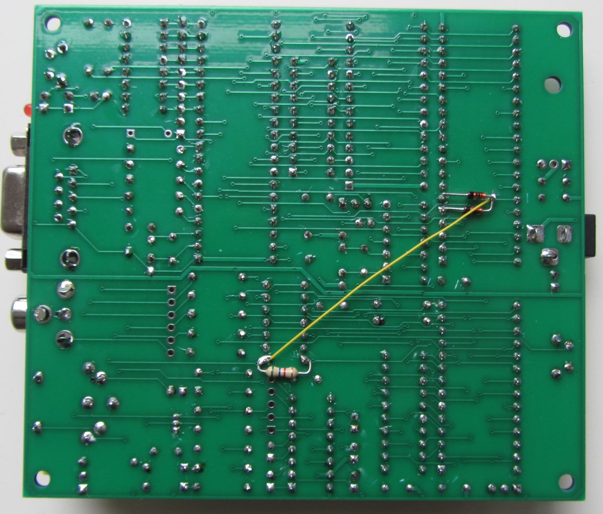
Fix for firmware version 7.11
This is the description of the fix for the 7.11 firmware but will break the 5.21 firmware. An unmodified 0.10 board will work with the 5.21 firmware. With the fix in place, disconnecting the diode from pin 6 will restore the original situation.
The cathode of the diodes is where the band is (usually black or white). The diodes I used were BAT85, but most generic small signal schottky diode will probably work.
Cut the trace between U5-5 and U8-2 (old HS)
Add resistor of 5.6k between U8-14 and U8-1 (pullup resistor)
Add cathode of 1st schottky diode to U5-5 (new HS, horizontal sync)
Add cathode of 2nd schottky diode to U5-6 (new VS, vertical sync)
Connect the anodes of the two schottky diodes (new CS, combined sync)
Add a wire between the two schottky diode anodes to U8-2
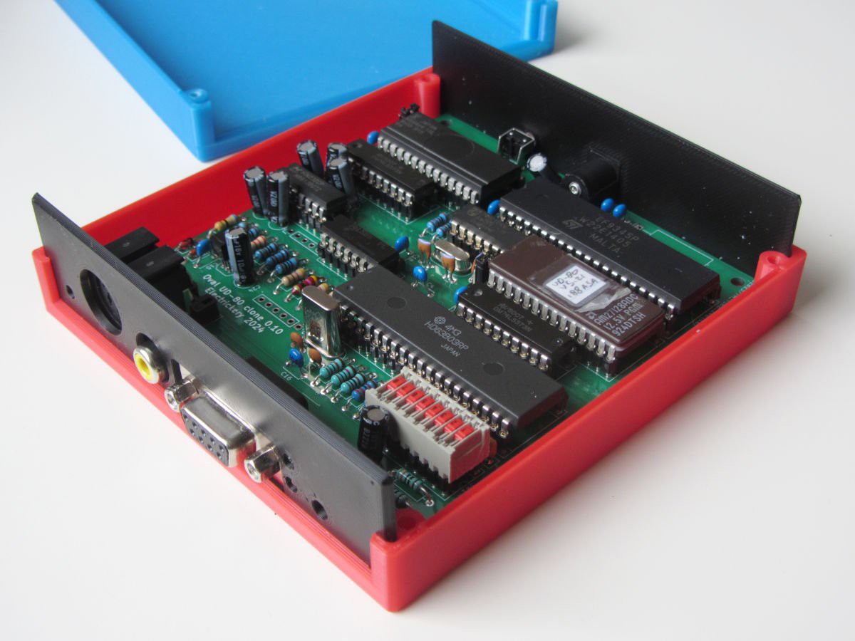
All the components are finally in and soldered to the new 0.10 board. It was mainly my poor component inventory management and distractions why it took so long.
Before testing the new board, I adapted the old 0.8 prototype to the new video circuit, and it looks quite good on my preferred display. Good enough to update the DIP-switche table:
ROM V5.21E:
1. off = 80 char./line, on = 40 char./line
2. ?
3. off = PAL, on = NTSC
4. off = white on black, on = black on white
5. ?
6. ?
7. ? 8. ?
ROM V7.11A:
1. off = NTSC, on = PAL
2-8. ?
The 7.11A version uses the DIP switch only for video mode. At least the 40/80 column mode is moved to software as it is mentioned in the ROM dump. This ROM also contains the intriguing text: "System Utilities Screen".
The 5.21E ROM version configures the EF9345 HS pin for both horizontal sync and vertical sync.
Board update
The 7.11A version uses both the HS and VS pins. This requires a small modification on both the old 0.8 and new 0.10 board for the 7.11A version.
 fjkraan