Skyhawkson
-
Traces and Nets and Pads, Oh My!
02/05/2024 at 21:53 • 0 comments![]()
Yeah, yeah, it's Paint3D. It's better than you think, I swear! With our components pretty much resolved, it's time to answer the question of "how does everything go together?" Well, the step in that is to get a map of the nets on the board, and start assigning them names. Ideally all this info would be captured in schematic form, using a program like KiCAD's EESchema or (🤮) AutoCAD Electrical, but without a solid understanding of what we're looking at here, it's tough to know where to begin.
The Process:
Borrowing a trick from my favorite random electronics disrepairman BigClive, I took high res photos of the front and back of the boards, isolated them onto a white background, and mirrored the backside. There aren't any designators there anyways, and this gives us a picture that's far easier to mentally process, similar to looking through all layers of a PCB in KiCAD's or Altium's layout modes. Since we have no top traces, I only needed to map out traces on one side, so I picked up my bucket and line tools and began filling in all attached nodes to individual nets.
Net Naming:Unfortunately, we have a couple problems. The board designers weren't kind enough to give us a list of signals in the connector, a pin 1 marking, or even a ground plane. We'll have to make some assumptions:
1. Pin 1 on the connector is marked by the green line on the top layer
- We can't possibly know this, but I need some sort of reference2. There are/may be multiple power inputs and returns. We can't trust that only one ground exists
3. This board may be multi channel
- While we don't know the exact function, we can't assume uniqueness or a lack thereof. All nets should be treated independently.4. The board may be AC, DC, or a mix of both
- I'll use the phrase 'power' and 'ground/return' a lot, but there's no actual reason to believe this is DC at this point. I just do it out of habit/convenience.Not very helpful to our investigation, I know. But we have to start somewhere, so we'll name the gold fingers on the edge connector Pins 1 thru 21, name their nets accordingly, and index the remaining nets from 22 onward.
The Result:
After a lot of tedious drawing and labelling, the shape of the board starts to emerge:
![]()
It appears we're looking at 36 unique copper nets, with very few similarities or repeats in shape and design. Hard to deduce anything immediately, but this will give us a basis for a better diagram in KiCAD, and then a SPICE simulation. I have a few observations of my own:
- NET 21 connects to a large number of components and could be a power rail of some kind.
- NET15 thru NET21 are all similarly fanned out, and could be part of a common power or ground bus.
- NET2 connects to both sides of a trimpot, as does NET23 and NET 24. They all probably have the same functionThe next step in the project is to turn this jumbled mess into a proper (or proper-ish) schematic. For that, it'd be a massive help to have a view where we can see all nets and components at the same time. Fortunately, with the magic of transparency...
![]()
With that, it's time to get stuck into some schematics.
-
Components List (Mostly) Complete!
02/04/2024 at 18:46 • 0 commentsFirst step in any reverse engineering process is pretty simple - "What the heck are all of these parts?"
Thankfully, the designers were kind enough to label everything, and while the conformal coat has yellowed with age, it's not completely opaque. So what have we got? Well, an assortment of the following prefixes:R: easy, simple resistors and three trimpots
Q: Transistors, and in lovely labelled cans for convenience
CR: Now that's not a reference I've ever seen used, but a quick Wikipedia reference says 'Diode'. Simple enough.For the most part, this board is pretty considerate to the reverse-engineer. Almost all components are bent such that their PN#, value, or significant characteristics are upright. The conformal coat has browned with age, but is still generally translucent. And while 60+ years of dust and cigarette smoke has left some grime in between components, it mostly wipes off with a paper towel and some 99% isopropyl alcohol. But we still have a few oddities to resolve...
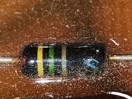
Oddity #1: CR103 and CR104![]()
Get a load of that grime At first glance, a couple of three-stripe, two-lead, all-black components screams "I'm a carbon resistor" with a 20% tolerance. In this case, YEL-GRN-BRN would make it a 450Ω 20%, which is in family with the rest of the board's values. But that's an odd choice; this is a nice board with a bunch of mil-spec resistors, many of which are higher-than-average power rating (up to 3W), and the 'CR' marking still indicates this is probably a diode of some kind. So what gives?
![]()
A little bit of cleaning gives a better (albeit still-dusty) picture. We can see the color bands are probably actually YEL-GRN-GRY, that the body is actually made of glass, and there's a mysterious blue 'S' printed on one end of the device. It was here I learned that back in the day, '1N'-series diodes were often marked with the same color bands, making this a 1N458. I'm still not sure what the 'S' was for, but that seems like our winner.
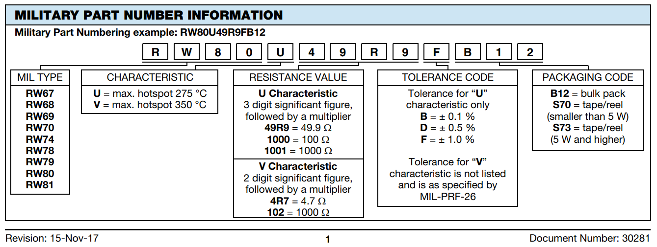
Oddity #2: RW-59 and MIL-R-26
![]()
Check out those gorgeous Texas Instruments TO-5 transistors! All of the large, purple resistors on the board are labelled with the same "RW59 V___" numbering scheme. Not as convenient as color bands or directly writing the specs on the resistor (as DALE so helpfully did on a handful of devices on the board) but it gives us somewhere to start. A quick search indicates these are probably part of the MIL-R-26F standard, which unfortunately isn't available from many reputable sources online and doesn't define an RW59 number. RW59 seems to be entirely relegated to old Ohmite parts, at least if ebay listings are anything to go by, and they have no public info on them. Helpfully, however, Vishay still has plenty of data on other RW-series items, conveniently available on their website, and it seems safe to use this to decode the parts in front of us.
![]()
Thanks Vishay! Given that decoder chart, we can make educated guesses for all resistors in the series. I've included the list of known information in the project files and github.
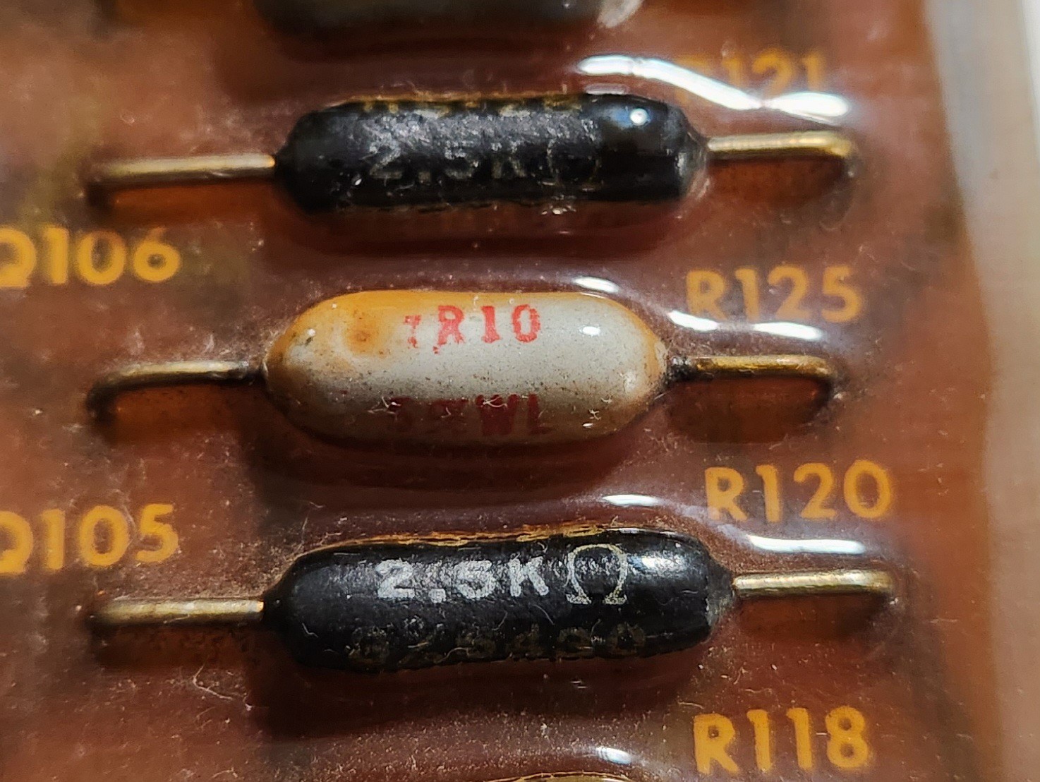
Oddity #3: R125
![]()
R125 is an unfortunate case of old conformal coat obscuring exactly the information I need. While it's also an RW59-series resistor (from what I can see poking up from the conformal coat on the other side), the first digit is completely obscured.
For now, about all we can guess about it is that it's a low resistance (the _R10 implies is a _ .1Ω resistor) and we can see that it's marked 5%. Probably a low value item; it could even be a .1Ω. We'll have to see how it fits in the context of the circuit to make a better guess; I'm trying my best not to damage the board during the reverse engineering process.
Reverse Engineering an Apollo-Era Circuit Card
This is the oldest PCB in my collection, acquired from a scrap sale at an old NASA test stand. What did it do?