Jara
Jara-
Beware of Non-Legit Indiegogo Campaigns
01/05/2025 at 20:37 • 0 commentsThere is an ongoing Indiegogo campaign called “X65GS 65816 Gaming Console“, see screenshot below.
I – as the creator of the x65 project – do not support and do not endorse this campaign.
In the campaign page they reused my own ‘amateur’ photos of that one x65-sbc device, which is right now on my work-desk at home. IT MEANS: they do not have the capacity or knowledge to produce own replicas of the x65-sbc computer for testing and marketing purposes, yet they have the guts to request money from unsuspecting customers!
Think twice before parting with your money. The funding mode ‘Flexible Goal’ (= This campaign will receive all funds raised even if it does not reach its funding goal.) is also telling.
![]()
Since the x65 project is open-source, with all sources and documents available in public github repository, anyone can build their own device. Theoretically, a commercial company could bring the device to market, though I would be rather happier if they cooperated with me before the attempt. Building one replica of the device for personal use may be hard. Making it a series product is on an entirely different level of hardness!
Why do I care about this? Because of my personal brand. When the campaign takes money but fails to deliver goods (or delivers only poor quality of thereof), the unhappy customers will be after me. Or another scenario: when the organizers receive money, they come to me and say: hey Jaroslav, we have money, build us XX pieces! If you won’t, you make lots of people unhappy about your project… and that would be an extortion.
https://www.jsykora.info/2025/01/beware-of-non-legit-indiegogo-campaigns/
-
New x65 Debugger in the textual Framework
01/05/2025 at 20:30 • 0 commentsI started a new debugger tool for my x65 project. Previously I created a dozen of single-purpose python scripts (running on a linux PC) that let me single-step the CPU, read CPU registers, dump memory and so on. The scripts use a common ‘backend’ modules to connect to the x65 hardware over the USB / FTDI interface, but otherwise each script acts on its own.
These python scripts and modules are located in the project subdirectory x65pyhost:
cpuidec.py disable-abrt02.sh do-cpustep.py do-loadbin.py do-poke.py do-vchartest.py do-vlogo.py cpuregs.py do-cpureset.py do-dump.py do-loadprg.py do-readregs.py do-veradump.py enable-abrt02.sh x65ftdi.py dbg.py do-cpurun.py do-i2cdump.py do-memtest.py do-savebin.py do-videotest.py icd.py vera.py
Some of the scripts were demonstrated in my previous post: Reading of 6502/65816 CPU Registers by a PC-based Debugger.
The new debugger tool, called very unimaginatively ‘dbg.py‘, will integrate all functions. It will work as a stand-alone full-screen debugger on the PC host. For the User Interface I decided to use the python framework ‘textual’. Textual is a cross-platform GUI (or rather TUI = text user interface) library which lets me create rich interface while staying in a text console.
The following screenshot shows the current (very early) state of the debugger. The debugger is running on linux PC in a window terminal. The program communicates with x65 board over the USB interface. The screen is divided in two halves. On the left side there is an instruction trace from the CPU (each line is one CPU cycle; instructions typically execute in 2-4 cycles). On the right side there is the current CPU register contents. The empty space on the right will be probably filled with configurable memory dumps and other settings.
![]()
-
A small step: New Font for the Enclosure
11/28/2024 at 20:54 • 0 commentsI did not quite like the original font that I have chosen for the enclosure text in the previous post. It just looks too ordinary:
I wanted something a bit more futuristic, with clear simple lines and curves. Finally I have chose the font called Dune Rise (available on dafont.com):
![https://www.dafont.com/img/preview/d/u/dune_rise1.png]() According to font's author: Dune Rise is a futuristic display font that draws inspiration from the title of the science fiction film "Dune," directed by Denis Villeneuve. Jesta Designs from Fontswan.com created this font using the Canadian Aboriginal syllabary as a basis, which is believed to be the same approach used for the film's logo design.
According to font's author: Dune Rise is a futuristic display font that draws inspiration from the title of the science fiction film "Dune," directed by Denis Villeneuve. Jesta Designs from Fontswan.com created this font using the Canadian Aboriginal syllabary as a basis, which is believed to be the same approach used for the film's logo design.
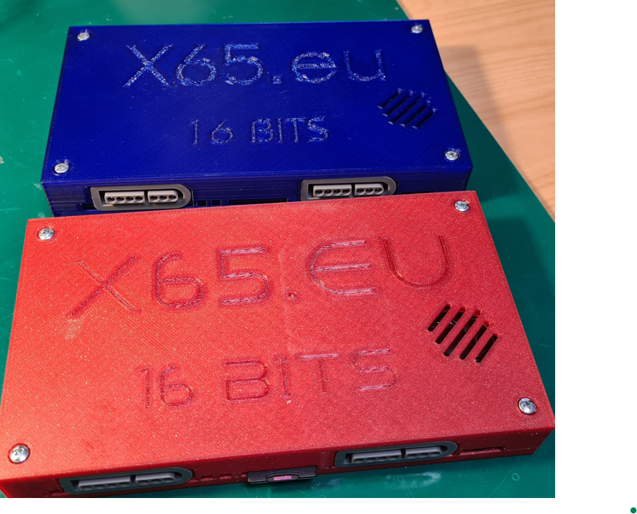
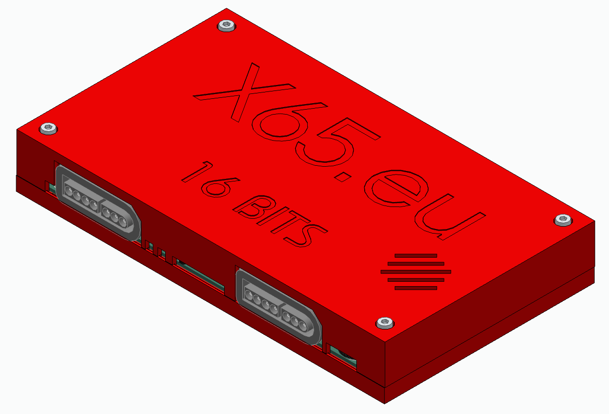
I printed the new variant in a red PETG which unfortunately does not look the best in photo below. The blue one is the original font, the red one is new:(I could also make it turn :-)
![]()
-
Enclosure
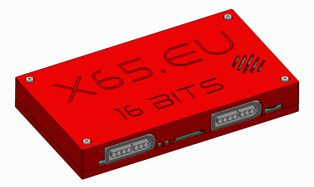
11/17/2024 at 20:23 • 0 commentsI designed an enclosure box for the x65-SBC computer. For modelling I used Siemens Solid Edge 2024 CAD software, of which I have the Employee Edition. (I think it is just similar to the free Community Edition, but I did not verify.)
![]() The enclosure box is composed of 'top' and 'bottom' parts which can be 3d-printed individually. The parts are screwed together with four M3x25 screws and M3 nuts, with the PCB held in the middle:
The enclosure box is composed of 'top' and 'bottom' parts which can be 3d-printed individually. The parts are screwed together with four M3x25 screws and M3 nuts, with the PCB held in the middle:![]() For the first print I have used a Prusa's Carmine Red PETG filament on my MK4. Here are photos of the front and back views:
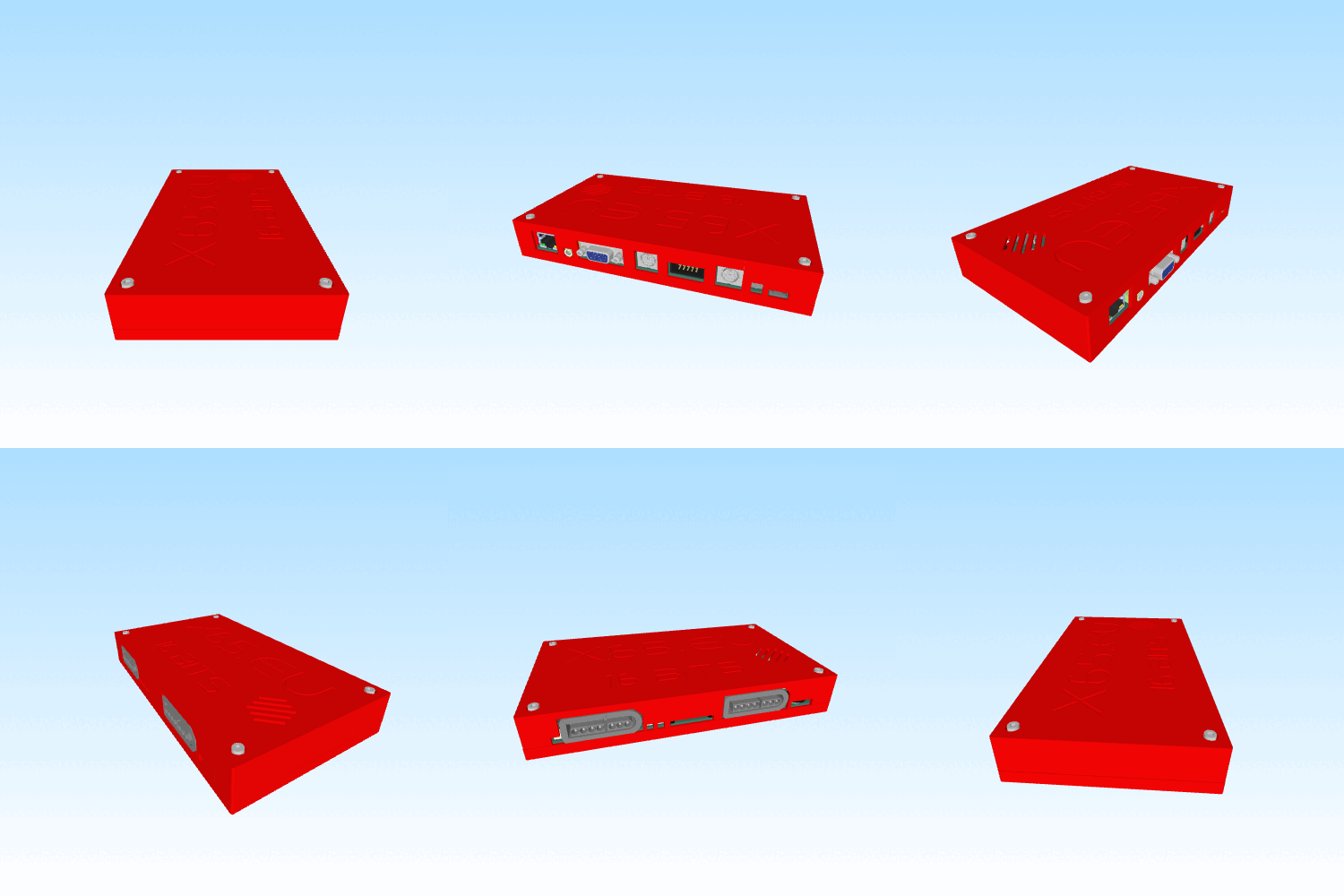
For the first print I have used a Prusa's Carmine Red PETG filament on my MK4. Here are photos of the front and back views:![]()
![]() The mechanical fitting of the PCB to the box is surprisingly good. Following picture is a cut-away view with the SNES connector on the front and VGA connector at the back:
The mechanical fitting of the PCB to the box is surprisingly good. Following picture is a cut-away view with the SNES connector on the front and VGA connector at the back:![]()
![]()
I implemented shadow lines at the interface between the two box parts, shown in the picture above. Shadow lines help the two pieces to come together and make for an optically "clean"
All files are available in the repository github.com/jsyk/x65-mech.
And this is another print in Ultramarine Blue PETG:
![]()
-
Dreamtracker’s Rabbit Hole
10/26/2024 at 13:26 • 0 commentsAs mentioned in previous post, Matej asked me if Dreamtracker app is running on X65. I told him that yes, it should run, but better to test it first myself. I downloaded Dreamtracker in its current version V0.71, fired it up, and well, after a promising start – I could see its main menu for a split second – the program crashed into the Monitor…. Well, that felt embarrasing 😮
This youtube video shows the crashed start:
![]()
The Monitor screen indicates the crash was caused by executing a BRK instruction. In 6502 CPU the BRK instruction has the opcode $00, and the value is typically used as a filler byte in empty regions. The PC=0xFEAC and RO=0x00 indicates the instruction was executed at a location near the end of the first ROM bank.
I wanted to see exactly from where the CPU came to this instruction address. I don’t know how to do that on a regular 6502-based system, but on my X65 it was not so difficult. NORA FPGA already has a built-in In-Circuit Debugger (ICD). The ICD monitors instruction stream executed by the CPU in real time and stores instruction trace in a 512-element ring buffer, which could be read out to a PC over the USB link any time. NORA can also send ABORT signal the CPU when specific conditions in the instruction stream are encountered. Therefore, all I needed was to (temporarily) modify ICD in the FPGA to stop the CPU clock when the BRK opcode (0x00) is executed. This was done and these are the last seven instructions before the faulting BRK opcode:
Cyc #  -25:  MAH: 0 (low :  0)  CBA: 0  CA: 3c3  CD:68  ctr:1f:----  sta:7f:r--emxPDS     PLA
Cyc #  -21:  MAH: 0 (low :  0)  CBA: 0  CA: 3c4  CD:85  ctr:1f:----  sta:7f:r--emxPDS     STA $01
Cyc #  -18:  MAH: 0 (low :  0)  CBA: 0  CA: 3c6  CD:68  ctr:1f:----  sta:7f:r--emxPDS     PLA
Cyc #  -14:  MAH: 0 (low :  0)  CBA: 0  CA: 3c7  CD:40  ctr:1f:----  sta:7f:r--emxPDS     RTI
Cyc #   -8:  MAH: 1 (low :  1)  CBA: 0  CA:372c  CD:a9  ctr:1f:----  sta:7f:r--emxPDS     LDA #$08
Cyc #   -6:  MAH: 1 (low :  1)  CBA: 0  CA:372e  CD:20  ctr:1f:----  sta:7f:r--emxPDS     JSR $feab
Cyc #    0:  MAH:41 (RomB:  0)  CBA: 0  CA:feab  CD: 0  ctr:1f:----  sta:7f:r--emxPDS     BRK #$00
Let’s have a look at the instructions. The first four must be a part of an interrupt handler which ends with RTI, Return From Interrupt. Then we have “LDA #$08” which loads the value 0x08 into Acumulator register and “JSR $feab” a Jump to Subroutine at the address 0xFEAB. At this address the processor encounters the BRK instruction and NORA has stopped it. It really looks that the jump to $FEAB in ROM is intentional in the Dreamtracker code. So I searched the Dreamtracker code source and I found it pretty quickly: in the file x16.inc there are the following definitions of jump addresses:
    ...
    SCREEN_SET_MODE        := $FF5F
    SCREEN_SET_CHARSET        := $FF62
    screen_set_charset          := $FF62
    extapi            := $FEAB    <=== HERE
    i2c_write_byte        := $FEC9
    I2C_WRITE_BYTE        := $FEC9
    entropy_get            := $FECF
    ....
Evidently $FEAB is supposed to be
extapiin the ROM. We can find several references toextapithroughout the dreamtracker code, for example here in the main:; Check for input from the keyboard, and do something if ; a key was pressed (return value is something other than 0) check_keyboard: ;sei ; call ps2data_fetch lda #$08 jsr extapi <=== HERE jsr SCNKEY jsr GETIN ;keyboard beq main_application_loop sta zp_KEY_PRESSEDI searched
extapiin my copy of X16 ROM sources, and found none. Then I searched for $FEAB and found it invectors.s:; *** this is space for new X16 KERNAL vectors *** ; ; !!! DO NOT RELY ON THEIR ADDRESSES JUST YET !!! ; .byte 0,0,0 ; $FEA8 .byte 0,0,0 ; $FEAB <=== HERE :-( .byte 0,0,0 ; $FEAE jmp mciout ; $FEB1 jmp i2c_batch_read ; $FEB4Oh, evidently the vector is not used – in my copy of the ROM. I updated to the latest CX16 ROM version R48 and there it was – the
extapifunction is now defined at that specific address!; *** this is space for new X16 KERNAL vectors *** ; jmp extapi16 ; $FEA8 jmp extapi ; $FEAB <=== HERE :-) .byte 0,0,0 ; $FEAE jmp mciout ; $FEB1 jmp i2c_batch_read ; $FEB4Now I was pretty confident that after a ROM update in the X65 computer the Dreamtracker would start.
In X65 a ROM update is done from a Linux PC via the USB connection, no additional HW necessary. You could either download the released (already compiled) ROM file from CX16 git repository, or you could build it yourself from the sources. In later case the output file rom.bin is found in directory x16-rom/build/x16. In any case this rom.bin file must be copied into x65’s repository directory sw-spiflash/sbl-for-cx16 (or you could modify variable CX16ROM in Makefile in that directory), and after that you must run
maketo wrap it:jara@megalit:~/hw/Open65/sw-spiflash/sbl-for-cx16$ make ca65 -I../../include -I. --cpu 65c02 ../common/../common/sbl.s ca65 -I../../include -I. --cpu 65c02 ../common/../common/isafix.s ca65 -I../../include -I. --cpu 65c02 ../common/../common/vidtext.s ca65 -I../../include -I. --cpu 65c02 ../common/../common/font8x8.s ld65 -C ../common/sbl.ld ../common/sbl.o ../common/isafix.o ../common/vidtext.o ../common/font8x8.o -o sbl.bin ca65 -I../../include -I. --cpu 65c02 ../common/sbl.s -l sbl.lst ca65 -I../../include -I. --cpu 65c02 ../common/isafix.s -l isafix.lst ca65 -I../../include -I. --cpu 65c02 ../common/trampoline.s -l trampoline.lst cat sbl.bin rom.bin >img.bin
This sequence has built a Secondary Bootloader (SBL) for X65 and appended CX16 ROM as SBL’s payload. The SBL provides a splash screen while the CX16 “ROM” is loading, and a startup wrapper code to kick off the CX16 “ROM” in correct parts once it has been loaded in the X65 RAM. The next step is to write the complete file
img.bininto the flash memory of X65. This is done bymake prog_imgas follows:jara@megalit:~/hw/Open65/sw-spiflash/sbl-for-cx16$ make prog_img ../../x65prog/x65prog -N -o 256k img.bin init.. cdone: high reset.. cdone: low flash ID: 0xEF 0x40 0x15 0x00 file size: 253952 erase 64kB sector at 0x040000.. erase 64kB sector at 0x050000.. erase 64kB sector at 0x060000.. erase 64kB sector at 0x070000.. programming.. done. reading.. VERIFY OK cdone: high Bye.
With the R48 ROM ready and flashed in the X65 computer, I did not expect further problems. What a surprise then, when it did not boot at once!
After some head-scratching and google-googling, I had a hunch that this problem might be related to CX16’s latest addition of the support for the 65816 CPU. The discussion in this thread tells us how the ROM newly distinguishes between the 6502 and 65816 processors. It is using the following instructions in hex: $18, $E2, $01. The code is interpretted by 65c02 as:
CLC                 ; clear carry flag
NOP  #$01           ; a 2-byte no-op
While 65c816 interprets the same code as:
CLC                 ; clear carry flag
SEP  #$01           ; sets bit 0 of the processor status register, which is the carry flag
The resulting carry flag is zero (cleared) on 65c02, and one (set) on 65c816. Any code that follows can use this information to possibly switch the processor in 16-bit mode, if 65816 has been detected, or use an alternate 8-bit code on 6502.
In case of X65 I got some in-between behaviour. The ROM apperantly detected that it is running on 65816, and then did something unexpected – which I have not so far had the time to investigate. Sorry! There is an information in the CX16 thread that no addressing into different bank than the BANK $00 takes place, but one could not be sure. The original CX16 does not decode the BANK bits of 65816, so a program bug in this case would go invisible.
To get the latest ROM running quicky while not spending my time an another annoying reverse-engineering task at that point, I got creative and hot-fixed the issue in the NORA FPGA. The FPGA has already support for observing the processor instruction stream as it is going, and throwing an ABORT exception whenever a “banned” instruction is about to execute. “Banned” are attempts to run 65816-only instructions while the processor is in the Emulation mode. So far I have used this feature to filter out the RMBx, SMBx, BBRx and BBSx opcodes, which have a completely different meaning in 6502 versus in 65816. For these instruction NORA FPGA raises the ABORT exception in the 65816 processor, and a handler emulates the “banned” instruction step-by-step in software code. Newly I have added the opcodes $E2 (SEP xy) and $C2 (REP xy) to the list of banned opcodes in the Emulation mode. (Note that when the 65816 is in the Native mode (8-bit or 16-bit), no opcodes are banned by NORA – we assume clean code then). Exception handler for banned instructions has been updated to just skip the 2 bytes ($E2 $xy, and $C2 $xy), thus exactly emulating the behaviour of 6502 on 65816 processor in Emulation mode as NOPs. This way we fool the CX16 ROM in thinking it is runing on the “good old” 6502, and it attempts no switching into the Native mode. And yes, after this FPGA hot-fix the ROM started with no problems. We will investigate why it had failed sometime later.
Finally I could run Dreamtracker 0.71 and amuse myself with some of its tones:
So yes, Dreamtracker V0.71 with CX16 ROM R48 runs well on X65.
-
The X65 Saga Continues
10/03/2024 at 18:34 • 0 commentsIt's Autumn again and I am revisiting my Project X65. My list of to-do tasks is endless and growing still :-)
* finishing tests of the A1 prototype
* load BOM to Mouser
* testing the USB interface
* better ESD concept
* indication of stopped CPU
* consider new extension connector
* consider if SDMMC power should be switched
* feasibility of machine assembly of prototypes
* check the new SMC code in CX16
* check the new 65816 code in CX16
* In-Circuit Debugger (ICD): describe in a post, add breakpoints support, describe ISAFIX, implement GUI for debugger...
* 3D box design...
* posibilities for own software besides CX16: Forth OF816 (partly implemented), Fastbasic, Mad-Pascal, GeckOS...
* update x65.eu landing page
* and so forth...During the summer I have received a couple (2) of emails with comments: by Eric from France and by Matej from Slovakia.
Eric would preffer the X65 in an ATX form-factor: an X65 ATX motherboard that could be inserted in a standard PC case, with many extension slots for plugging of extension cards. He would like to use such computer for automation. He could develop control programs in Basic or C, and he plans to develop own expansion cards: mainly for communication but also for audio processing. The computer would be used as an input/control/display front end.
The PMOD connector, which the X65 SBC supports in HW, is not stackable and lacks mechanical fixing points. It is not suitable for deploynment of an application to a customer and it is very "timid" opening to the outside world.Matej owns Atari 130XE with many extensions (1MB RAM, 2x Pokey sound, SD-Drive, VBXE graphics card).
He is interested in CX16 but he is disappointed with low availbility/long waiting times in the e-shop and relatively high cost. He is interested in running Dreamtracker on CX16. He can write software in MadPascal. He offered to design a 3D-printable box for X65. He requests if I could send him a prototype of the X65 SBC; we agreed that I would build one for him for the cost of components. -
Video-Terminal for the Forth OF816 Interpreter
04/09/2024 at 19:43 • 0 commentsIn the previous post I have mentioned that I am working on a port of the 32-bit Forth interpreter OF816 to my X65-SBC, an 8/16-bit retro computer that I am building. The software runs on the X65-SBC in the 65C816 processor, but the user textual input and output was so far realized via the USB/UART interface terminated on a host PC in a terminal emulator (e.g. putty).
As the next logical step, shown in the demo below, I have implemented a video text terminal using the VERA chip and the VGA output from the X65-SBC. VERA is the computer’s video chip implemented in an FPGA. VERA has 128kB of internal VRAM and could be configured in various graphics modes, typically generating a 640×480-pixel resolution screen. For the purpose of a textual terminal output I am configuring VERA to display 80 columns by 60 rows of visible characters. Each character is 8×8 pixels, and each character can have one of the 16 foreground and background colors.
The following short demo shows the OF816 code running on the X65-SBC computer with the video terminal output from the VGA port (for the purpose of a youtube demo the VGA signal is captured in a PC and displayed in a live window). The text input to the OF816 software is (still) provided over the USB/UART (putty); this is a work in progress to utilize the PS/2 keyboard of the computer, next time.
Demo VERA Mode Configuration
VERA is configured in the 80x60 character text mode with this code snippet (65c02 assembly):
    ; DCSEL=0, ADRSEL=0
    stz   VERA_CONTROL_REG
    ; Enable output to VGA 640x480, enable Layer0
    lda   #TV_VGA | LAYER0_ENABLE
    sta   VERA_VIDEO_REG
    ; DCSEL=0, ADRSEL=0
    stz   VERA_CONTROL_REG
    ; characters are 8x8, visible screen 80 columns, 60 rows.
    ; Complete screen is 128x128 characters, 8x8 font
    ; # Layer0 setup: Tile mode 1bpp, Map Width = 128 tiles, Map Height = 128 tiles
     ; ==> 16384 tiles, each 2B => 32768 B
    lda   #MAP_WH_128T << 6 | MAP_WH_128T << 4 | BPP_1
    sta   VERA_LAYER0_CONFIG_REG
    ; map entries start at address 0 of VRAM, and occupy 32kB
    lda   #mapbase_va
    sta   VERA_LAYER0_MAPBASE_REG
    ; tile (font) starts at 32kB offset
    lda   #(tilebase_va >> 11) << 2
    sta   VERA_LAYER0_TILEBASE_REG
The “map” size is 128×128 characters (tiles), but only 80×60 is visible on the screen. Using registers VERA_LAYER0_HSCROLL_REG ($9F30) and VERA_LAYER0_VSCROLL_REG ($9F32) it is possible to smoothly scroll the 80×60 viewport over the larger 128×128 map. This feature is typically used in 2D scrolling games. VERA allows map widths and heights from 32 to 256 tiles (32, 64, 128, 256). Tile width and height could be configured to 8 or 16 pixels; for the textual display we use the 8×8 pixel tiles.
Memory requirements for the map are: 128 * 128 tiles = 16834 tiles. Each tile consumes 2 Bytes of the VRAM, for the total tile-buffer memory 32768 B = 32kB. VERA supports multiple Tile Modes that differ in colour depth and in the support for additional features (e.g. V-flip, H-flip). For the textual display the most suitable mode is the “Tile mode 1 bpp (16 color text mode)“, as described in the VERA documentation:
![]()
In this mode the first byte of each map tile is the 8-bit character index (ASCII code), and the second byte contains a 4-bit background and a 4-bit foreground colour of the tile. To display a text in the 80×60 characters screen grid you just set the character index and colours for particular tiles.
Font Data
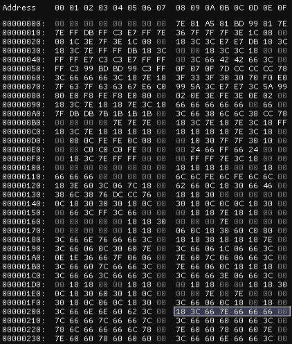
The 8-bit character index in each tile points to an 8×8-pixel “picture” (glyph) that shall be drawn at the tile position. This is the font data, and the font needs to be loaded in VERA’s VRAM during initialization phase. Each character in the font is 8×8 monochrome pixels, i.e. 8*8=64 bits, and that is 8 Bytes. The font has 256 ASCII characters, so the font data is 256 * 8 = 2048 B = 2 kB in total. The picture below shows the first 576 Bytes of the font that I am using:
![]()
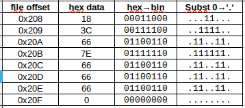
In the picture I have highlighted 8 Bytes at the position 0x208 to 0x20F: 0x18 0x3C 0x66 0x7E 0x66 0x66 0x66 0x00. Since each character glyph takes 8 Bytes of the bitmap, by dividing 0x208 by 8 we get the character index (ASCII code) for the glyph: 0x208 / 8 = 0x41 = 65 decimal, which is the capital ‘A’ letter. We can visually decode the glyph bitmap data in a spreadsheet by converting each data byte to its binary representation, and (for better visibility), replacing each ‘0’ with a ‘.’, as shown below. Now you can seen the bitmap that VERA would draw to the screen for each tile referencing the 65th character index.
![]()
Loading of Font Data to VERA in 65C02 vs. 65C816 CPU
The 2 kB font data must be loaded to VERA during each system initialization phase from a RAM. Let’s compare how this can be done in software of the X65-SBC, depending if the computer is equipped with the 8-bit 65C02 processor or the newer 16-bit 65C816 processor.
The first presented code snippet is for the 16-bit 65C816 processor:
.P816     ; this is a code for 65C816.
    ; configure addressing ptr at the font data (tilebase), autoincrement
    lda   #<tilebase_va
    sta   VERA_ADDRESS_REG
    lda   #>tilebase_va
    sta   VERA_ADDRESS_M_REG
    lda   #((tilebase_va >> 16) & 1) | (1 << 4)
    sta   VERA_ADDRESS_HI_REG
    ; configure CPU register widths:
    rep   #SHORT_I  ; 16-bit index regs X, Y
    sep   #SHORT_A          ; 8-bit memory and accu
    .i16
    .a8
    ; copy font data to VRAM
    ldx   #0                ; X := 0
loop_font_cp:
    lda   _font8x8,x        ; A := _font8x8[x]
    sta   VERA_DATA0_REG    ; store A to VERA VRAM
    inx                     ; X++
    cpx   #SIZEOF_font8x8   ; X compare with 2048
    bne   loop_font_cp      ; branch back if not equal.
After the VERA setup code at the beginning, which takes 6 instructions, the main copy loop (beginning at loop_font_cp) takes just 6 instructions. The highlighted loop is executed 2048-times, i.e. for each byte of font data.
Now lets have a look at the same program but implemented in the assembler for the 8-bit 65C02 processor:
    ; configure addressing ptr at the font data (tilebase), autoincrement
    lda   #<tilebase_va
    sta   VERA_ADDRESS_REG
    lda   #>tilebase_va
    sta   VERA_ADDRESS_M_REG
    lda   #((tilebase_va >> 16) & 1) | (1 << 4)
    sta   VERA_ADDRESS_HI_REG
        lda     #<_font8x8
    sta     PTR
    lda     #>_font8x8
    sta     PTR+1
    ldx     #0                 ; X := 0
loop_font_cp:
    ldy     #0                 ; Y := 0
loop_font_cp_inner:
    lda     (PTR),y            ; A := PTR[Y]
    sta     VERA_DATA0_REG     ; store A to VERA VRAM
    iny                        ; Y++
    cpy     #0                 ; compare Y to zero
    bne     loop_font_cp_inner  ; branch if not zero yet
    inc     PTR+1               ; PTR := PTR + 256
    inx                           ; X++
    cpx     #SIZEOF_font8x8/256   ; compare X to 2048/256
    bne     loop_font_cp          ; branch if not equal yet.
The copy loop starts at the label loop_font_cp. This time, however, we need two nested loops utilizing both the X and Y registers, and an additional 2 Byte variable PTR in the RAM (in zero page). The 8-bit X and Y registers together implement a 16-bit loop counter, in fact.
The cause of this “complexity explosion” in the assembler is the limited 8-bit width of all registers in the 65C02 CPU. To implement a loop that runs 2048-times, you need (for example) the X and Y registers, and then you need an additional variable to keep track of the source array position (the processor could do just 8-bit index, which is too less).
In comparison the 16-bit 65C816 CPU is much easier and efficient to program in the assembly language (at least in this case). The 2048-time iterated loop can run with just the X register, which is 16-bit wide now, leaving Y reg. unused, and utilizing a 16-bit indexed access (lda _font8x8,x) to get a byte from the font data into the accumulator. This coding efficiency is the reason why I prefer using the X65-SBC computer with the 16-bit CPU 65C816, and do not look back at the 65C02.
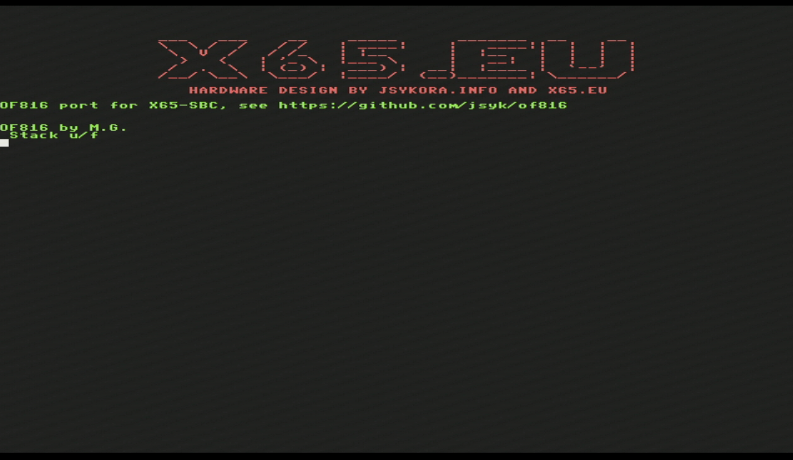
In the end I am relatively satisfied how the terminal output turned out. (Note below the inconspicuous error message “Stack u/f” from OF816 => there is more to explore here! 😎)
![]()
-
32-bit Forth for the X65 with 65C816 CPU
03/22/2024 at 21:11 • 0 commentsI am working on a port of the 32-bit FORTH interpreter OF816 for my X65-SBC computer with the 65C816 CPU. The OF816 was created by mgcaret and is available on github. I made a fork of the OF816 project and added a new branch for my work: x65-sbc.
The OF816 already supports a couple of 65C816-based systems: GoSXB, Apple IIgs, Neon816 and the W65C816SXB. I added a new subdirectory X65 in the platforms directory and initially copied from the Neon816 port, because it seemed the simplest.
The initial support for X65-SBC was not difficult to program. I modified the `_system_interface` routine in the `platform-lib.s` to work with the USB/UART registers that are implemented in NORA FPGA on the X65-SBC. After adjusting memory addresses in a linker script, I was surprised that this minimal OF816 port worked on the first try.
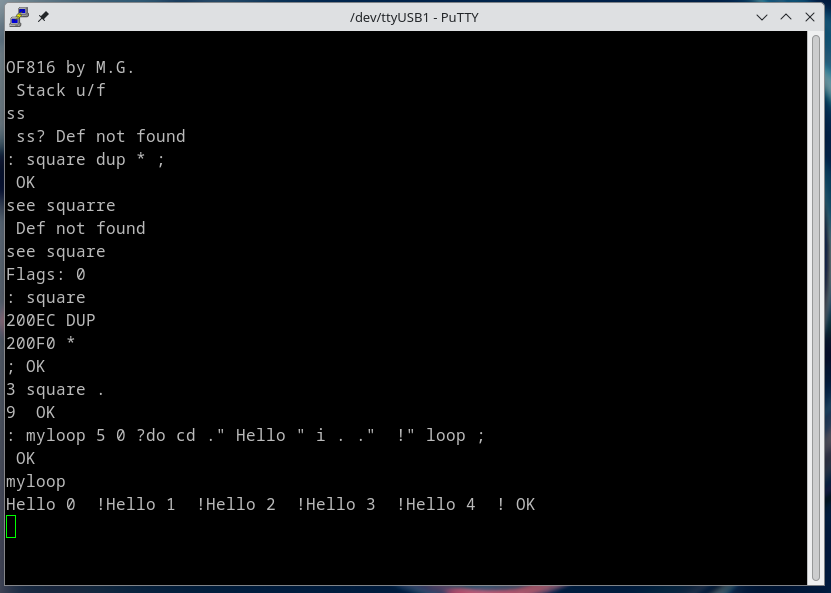
![]()
The screenshot above shows a terminal emulator on Linux PC connected over USB/UART to the X65-SBC computer running the OF816 FORTH interpreter. Since I am just a beginner in the FORTH language, it took me a few lines to enter and run a Hello World loop.
This OF816 FORTH port currently communicates over the UART on the X65-SBC. Therefore the user interface is on the host PC for now, and the keyboard and video output on X65-SBC are not utilized.
This is just temporary as I am already working on a basic virtual terminal (i.e. screen editor) for the X65-SBC and the first "client" will the OF816 interpreter. -
Reading of 6502/65816 CPU Registers by a PC-based Debugger
03/03/2024 at 20:08 • 0 commentsModern microcontrollers and microprocessors have built-in facilities for external debuggers to read/write registers, set breakpoints and generally fully control the CPU. This is one of the main usecases of the standard JTAG interface. The 6502 and 65816 CPUs were created more than a decade before the first version of JTAG was even defined. They contain no support for external debuggers whatsoever.
To overcome the lack of debugger support, the system bus controller "NORA" in X65 implements the necessary functions for a debugger running on a host PC (with Linux or Windows) and connected over the USB-C port. With this support in NORA a debugger can control the 6502/65816 CPU at the instruction level.
One of the basic functions of a debugger is to read out the contents of the programmer visible CPU registers. This log entry describes how this is done in the X65 computer. ....
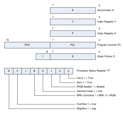
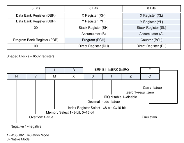
---------- more ----------For the 8-bit 6502 CPU these are: A, X, Y, S (= SP) (all 8-bit), PC (16-bit), and flags (8-bit); shown below:
![]()
For the 16-bit 65816 CPU these are: A, X, Y, S (= SP) (all 16-bit), PC (24-bit), DBR (Data Bank Register, 8-bit), Direct Register (DH:DL, 16-bit), and the flags (8-bit); shown below:
![]()
Block Diagram of NORA's In-Circuit Debugger (ICD)
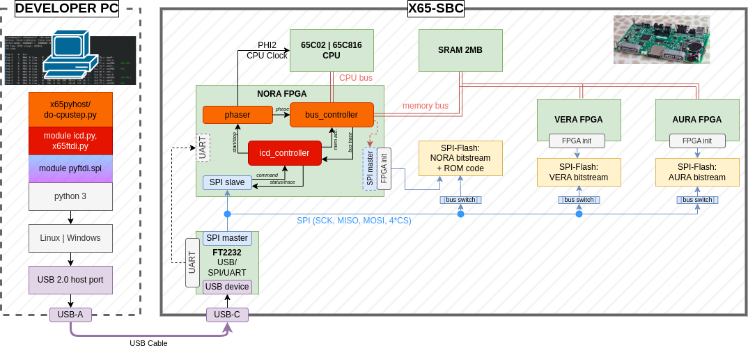
The block diagram below shows the concept of the In-Circuit Debugger (ICD) in the X65 computer. NORA FPGA implements all interfaces between the 65xx CPU, and the memory bus with SRAM, VERA and AURA FPGAs. The particular verilog module in NORA that implements the CPU/memory interface is called bus_controller. Another module, the phaser, generates the CPU clock signal PHI2 and additional internal timing signals that must be in sync with the CPU execution. The third module mentioned in the picture is the icd_controller which controls the bus_controller and phaser during debug sessions, and during system startups, but othertimes it is idle.
![]()
The icd_controller itself responds to commands received from an SPI Slave port, which is connected to physical SPI pins on the FPGA (signals ICD_CSn:in, ICD_MOSI:in, ICD_MISO:out, ICD_SCK:in). These pins are connected on PCB to the FTDI USB/SPI+UART converter (FT2232H), and from there via a USB cable to a host PC with a debugger software.
Debugger software for X65 is implemented in Python 3 (with the pyftdi module) and it is available in the
git repository in subfolder x65pyhost. For simplicity of development, debugger commands are not yet integrated in an IDE but they are available as individual programs called from a command line.
The most commonly used commands (= python scripts) are listed in the table:Command (script) Description do-cpureset.py Reset and stop the 65xx CPU do-cpurun.py Run the CPU do-cpustep.py Stop the CPU and step it for the given number of instructions or CPU cycles do-dump.py Memory dump (including IO areas) do-loadbin.py Load a binary from specified host file into X65 memory do-loadprg.py Load a C64/CX16 program from a .PRG file into X65 memory do-poke.py Write memory location in X65 memory (incl. IO area) do-readregs.py Read CPU registers (the CPU must be stopped) Register Reading Sequence
Reading of 65xx CPU internal registers is implemented in the do-readregs.py and do-cpustep.py scripts that communicate with the ICD module in NORA FPGA over the USB/SPI bridge implemented on the PCB of X65 computer. Lets discuss how the registers are obtained from the CPU by NORA. As mentioned previously, the 65xx CPUs have absolutely zero support for external debuggers wishing to access internal registers outside of a program running in the processor.
The access is gained by forcing a predefined sequence of instructions to the CPU and observing signals on the CPU Data and Address Buses. At each CPU cycle, the 65xx processor accesses the external memory for either a read or write. By observing CPU status signals VPA and VDA (or SYNC), it is possible to determine if any given cycle is an opcode fetch. If it is an opcode fetch cycle, the debugger can instruct the ICD in NORA to force an alternative opcode to the CPU than what would be read from a memory, thus altering the program flow at will.
The following instruction sequence is forced from the debugger to read out all registers:
orig_pc:
    PHP             ; we get PC, SP, Flags
    PLP             ;
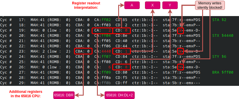
    STA $2          ; block writes; We get A, and on 65816 we get B depending on flag M, and we get DH:DL (DPR) on address bus
    STX $4440       ; block writes; We get X, and on 65816 we get XH depending on flag X, we get DBR from CPU Bank Address.
    STY $6          ; block writes; We get Y, and on 65816 we get YH depending on flag X
    BRA orig_pc     ; jump back to the back to leave CPU registers in the original state
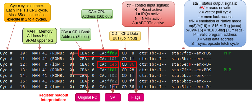
The code (PHP-PLP-STA-STX-STY-BRA) is position-independent: it could be execute at any CPU state. The first two 65xx instructions are *PHP* (Push Flags to Stack) and *PLP* (Pull Flags from Stack). NORA captures the trace of the the CPU Data Bus, Address Bus and Status signals while these instruction execute and the debugger uses the trace to reconstruct the original PC (Program Counter) address and the SP (Stack Pointer) address, and the flags register.
Screenshot below shows the trace output of *do-cpustep.py* (on Linux PC) when the 65xx CPU (actually 65C816 in Emulation Mode) is executing the opening PHP-PLP sequence. The screenshot is annotated at the top with explanations of trace columns, and at the bottom with the trace fields that correspond to exposed CPU internal registers:
![]()
The original PC (Program Counter) is the op-code fetch address of the first instruction. The SP (Stack Pointer) is the write address in the third CPU cycle (Cyc #12), and the CPU flags are the data value written to the memory at that cycle. The instruction PLP is necessary to restore the contents of SP inside the CPU to the original value.
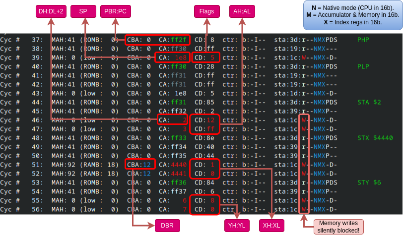
The next screenshot shows the trace of the remaining instructions in the sequence: STA-STX-STY-BRA. The contents of registers A, X and Y is obtained from the data bus write cycles during the execution of the STA (Store Accumulator), STX (Store X-reg) and STY (Store Y-reg) instructions. To not disturb the original memory contents by these writes, the memory write signal is silently blocked by NORA, although this is not reflected in the trace buffer.
![]()
The final instruction BRA (Branch Always) is necessary to restore the original contents of the PC register; it instructs the CPU to jump five instruction back.
65816 CPU
So far we discussed how to obtain registers from the 8-bit 6502 processor. The 16-bit 65816 processor has the common registers extended to 16-bits, plus it has some additional registers. The traces shown above were obtained on the 65816 CPU running in the 8-bit *Emulation Mode*, where the processor is behaving like the 8-bit 6502. (Emulation Mode is indicated by the "e" in the "sta" field of the trace. Mode information is available on an output pin of the processor.)
When the 65816 processor switches to the 16-bit *Native Mode*, the additional registers DBR (Data Bank Register), PBR (Program Bank Register, part of PC) and DH:DL (Direct (Page) Register) get activated. The traces above mark where these registers are exposed as well. Then, depending if the new M and X flags in the CPU Flag Register are cleared, also the Accumulator and Index Registers X/Y are extended to 16-bits. The M-flag controls the width of the accumulator (A -> AH:AL) and of the memory accesses (in all LD and ST-type instructions), and the X-flag control the widths of registers X (XH:XL) and Y (YH:YL). These three important flags (Emulation or Native mode, M-flag, and X-flag) are available on CPU pins, therefore they are always visible in the trace buffer.
The screenshot below shows the trace of the sequence PHP-PLP-STA-STX-STY in case the 65816 CPU is in the 16-bit *Native Mode* and also the accumulator and index registers are switched to the 16-bit mode (i.e. M-flag=0, X-flag=0). (The BRA instruction is not shown for brevity, but it is also part of the forced sequence.) We can see that the execution of the STA, STX and STY opcodes gains one additional CPU cycle during which the upper parts of the A/X/Y registers are written to the memory (these writes are blocked in NORA), and exposed for the debugger. The contents of the new address registers PBR, DBR, and DH:DL is meanwhile also available on the address bus.
![]()
Integration
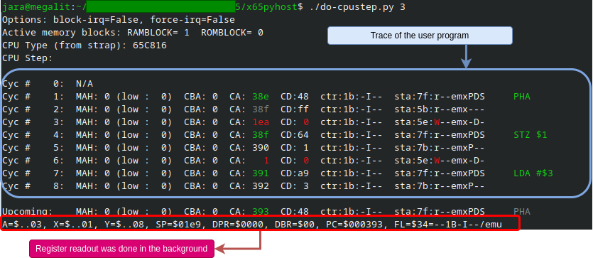
The complete register readout sequence is integrated in the script do-cpustep.py. This script dumps the 65xx CPU trace buffer and then executes a user-specified number of following instructions. Finally, the script executes the readout sequence in the background and prints the CPU register values. The forced readout sequence is not shown in the printed trace, of course.
The screenshot below shows the user interface when the command "./do-cpustep.py 3" (step for 3 instruction) is started on a Linux host PC connected with a USB cable to the X65 computer. The last line is the CPU register contents after the last instruction executed (and before "Upcoming", which has *not* been executed yet, it is just the prediction of the debugger based on PC). Notice how the displayed contents of the A register ($03) in the last line corresponds to the LDA instruction (LDA #$03), and the contents of the SP register ($1e9) corresponds to the push-address in the first PHA instruction ($1ea = the SP is decremented AFTER pushing).
![]()
Conclusion
In embedded systems reading of processor registers via a JTAG connection from a host PC is the basic functionality that we take for granted. Using the "NORA" FPGA as the system controller in the X65 computer brings this functionality also to the world of 6502/65816 processors.
X65-SBC
Single-Board Computer based on 65C02 or 65C816 CPU with 2MB RAM, VGA graphics output, PS/2 ports, and high-quality sound.


 According to font's author: Dune Rise is a futuristic display font that draws inspiration from the title of the science fiction film "Dune," directed by Denis Villeneuve. Jesta Designs from Fontswan.com created this font using the Canadian Aboriginal syllabary as a basis, which is believed to be the same approach used for the film's logo design.