Yann Guidon / YGDES
-
eBTB v2.0
07/03/2024 at 01:13 • 15 commentsThe last log introduced a modified, explicit Branch Target Buffer. It has evolved again since then and is taking a new life of its own...
As already explained, it totally changes the ISA, the compiler strategy, the coding practices, almost everything, but it is able to scale up in operating frequency, or with CPU/Memory mismatch, provided the external memory works with pipelined transactions. The new ISA exposes some of this and lets the compiler handle parts of the overlapping of prefetches.
So the jump system works with two phases :
- The program emits a prefetch operation: this associates a jump address to a fixed ID. The visible ID is 3 bits, there can be up to 8 simultaneously ongoing prefetch operations. For each ID, there is one 8-instruction cache line that is stored close to the instruction decoder, for immediate access. It usually takes several cycles to fetch the desired line and store in in the BTB.
- The actual "jump" instruction selects one of these 8 lines (with the 3-bit ID in the instruction) and checks the (possibly complex) condition. If the condition is verified, the selected line is chosen as source of instructions for the next cycle, and the PC starts to prefetch the next line(s) in its double buffer.
You can see this system as exposing a register set dedicated to instructions addresses. Each register is a target, so let's call them T0 to T7. You can only perform an overwrite of these registers with a prefetch instruction, or a "loopentry" instruction for example : there is no fancy way to derail the CPU's operation.
Each line has one of 4 states:
- absent/invalid
- fetching/checking
- failure/error/fault
- valid
This system mirrors the already studied mechanism for accessing data memory, but the BTB is much more constrained : Each data fetch address is explicitly computed and stored into a dedicated "Address register" (in Y32: A0 to A7), which triggers the TLB and cache checks, such that "a number of cycles later" the corresponding data is available in a coupled/associated "data" register (in Y32: D0 to D7). The #YASEP already uses this split scheme for 2 decades now.
And now, a similar decoupling scheme is also provided in the Y32.
So we get 8 visible registers : they must be saved and restored through all kinds of situations such as function calls, IPC or traps... yet there is no way to read them back to the general register file. The only way to get them out and back in is with the control stack, which can save 2 entries in one cycle.
So the pair T0-T1 can be saved and restored in one cycle, for example : it seems easier to pair them as neighbours. A whole set of targets can be saved in 4 instructions, 4 cycles. It still consumes a half-line of cache...
All the pairs of targets can be freely allocated by the compiler, with some hints and heuristics: the short-lived and immediate targets would be in the high numbers (T4-T7) while targets for later would be in the lower addresses (T0-T3). This makes it easier to save the context across the functions, as the buffer would be defragmented and there are fewer chances to save a register that doesn't need backup.
...
Another thing I didn't mention enough is that the control stack (its neighbour) also has hidden entries in the eBTB. Let's say 8 more lines (or even pairs for the double-buffering) which are allocated on a rolling basis. The stack manages the allocation and prefetch itself. Usually, these hidden lines are a copy of the current instruction buffer and its double/prefetch buffer, so there is only need of prefetch when the stack is emptying.
...
But the v2.0 goes beyond that: it manages the call/return and others, without the need for explicit saving/restoring by discrete instructions. These spill/unspill instructions are still possible but they take precious space (hence time).
What call and IPC now do is accept a 2-bit immediate (on top of the 3-bit target, the condition flags, the base address...) to say how many pairs of targets to push/pop automatically on the control stack.
But each pop or push takes a whole cycle, right ? Call already takes some time to push the PC and the context/base address.
The solution (which might sound familiar to Duane for example) is with a register window. In our case of 8 targets, 16 actual lines are actually implemented and addressed in a circular buffer. This means that a "base index" is added to the instruction's 3-bit Target ID to get the actual number of the physical entry.
What call/return do is simply add their 2-bit amount to the base index (shifted by 1) to make new entries available, while the old entries (now out of reach) can get saved in the background on the control stack, during the following cycles.
The granularity of 2 entries per cycle simplifies a few things, such as the computation of the effective index of the target/line, since the LSB is not changed. The instruction provides 3 bits but only 2 must be added to the current index, which is 3 bits as well but the LSB is implicit. That's a matter of a few XOR at most, so not a critical performance hog, unlike with a more classical register set in SPARC for example.
- Addressing a line from an instruction's target ID field is relatively simple: of the 3 bits, the LSB is preserved (pass-though) and the remaining 2 MSB (0-extended) are added to the 3-bit Target Based Index. Carry out is not calculated, it's a simple wrap-around.
- call instruction : 0-extended 2-bit field is added to the 3-bit TBI.
- ret only pops the destination, then also re-executes the call instruction to see how many levels must be restored, as well as which base register to restore.
Initially I was thinking that the 3-bit Target Based Index should be saved in the PC's MSB but it is not necessary if the stack is correctly emptied/spilled on the control stack. This TBI could be any value as long as the data is appropriate on the lines. It's all relative so who cares now ?
The control stack has a more straight-forward, direct addressing scheme, with 3 bits in the PC's MSB, next to the type field.
A typical function call would look like :
; main function:
  pf.t7 subfunction ; (a 24-bit immediate and 3 bits for TID)
  ; .. fill with some useful work if available
  ; while target #7 is being prefetched
  call t7, condition, a6, 2
  ; t7 : target line 7
  ; condition : the call can be "always" or check some flags
  ; a6 : the context/base pointer for the current function, to be saved.
  ; 2 : save 2 pairs of target lines, for reuse later.
  ; ... the rest of the function


subfunction:
  ; ... do something
  ; all 8 of the target lines are available
  ;   and can be overwritten/spilled/unspilled if needed.
  ret ; (eventual condition)
That's ... quite short, right ? Of course I didn't show the passing of parameters, which are moved/prepared in the sequence just after the prefetch instruction.
The function may choose to spill 0, 2, 4 or 6 targets across the call. During traps and/or IPC, it should be possible to also spill all the 8 current targets.
The depth of 16 entries is just enough to make the system work OK. 32 entries would use a lot more room for a smaller speedup.
The other very cool thing about this "target window" system : you can repeatedly call a function and the intermediate targets will remain in cache, in the window, speeding things up even more. There is a small stacked context, not just on the control stack but also the eBTB. This increases cache hit rates, frees some memory bandwidth in repetitive cases without programming efforts...
-
Second sketch
06/26/2024 at 14:49 • 0 commentsI have the drawing somewhere but it's not very different from the first one. There are two significant changes though.
The first change is the "instruction buffer", ex-Instruction L0, now called "explicit branch target buffer" (eBTB). It's a big change that also affects the instructions so I'll cover it later in detail.
The second change is the instruction decoder that is now meant to decode 3 instructions per cycle, instead of two. It uses an additional third slot in parallel with the 2 other pipelines (each inside one glob) to process the control stack, the jumps, the calls, the returns, and other instructions of the sort.
I couldn't... I just couldn't resolve myself to make a choice of which pipeline had to be sacrificed or modified to handle the jumps. And the nature of the operation is so different that it makes no sense to mix the control flow logic with the computations.
Ideally, the instructions are fed in this order : Glob1-Glob2-Stack. Any "slot" can be absent, so the realignment is going to be a bit tricky, and it increases the necessary bandwidth for the memories (FSB and caches). But the ILP can reach 3 in some cases, and is better than if I mixed the stack decoder with the Glob2 decoder, as this would create slot allocation contentions.
So the overall effect is a reasonable increase in ILP, the glob decoders remain simple, a special dedicated datapath can be carved out for the stack's operation and the "control" slot only communicates with the globs through status bits.
...
The other change, as alluded before, is with the instruction buffers that cache the L1, which are now explicitly addressed (at least at a first level). Most jumps work with a prefetch instruction that targets one of the lines, then a "switch" instruction that selects one of the lines for execution (and may stall if absent yet).
I have allocated 3 bits for the line ID. That makes 8 lines for prefetching upcoming instructions for a branch target. More lines (4?) are also dedicated-linked to the control stack.
Another line is the PC, which is actually implemented as a pair of line for double-buffering.
A direct Jump instruction acts as a direct prefetch to the double buffer, but it will stall the pipelines.
The targets for function calls, loops, switch/case, IF, and others are easy to statically schedule a few cycles in advance most of the time, leading to an efficient parallelism of all the units. Then a variety of branch instructions will conditionally select a different eBTB line ID, which gets virtually copied into Line #0.
So the eBTB has 2+8+4 lines working as L0 with specific ties to other units. More are possible using indexed/relative addressing of the eBTB.
This scheme mimics what is already happening with the data accesses : the core is decoupled from the memory system and communicates through registers. Instead, here, there is no register even though the lines virtually count as 8 address registers. But you can't read them back or alter them.
- A given target line can only be set with a prefetch instruction.
- A target line's address can be saved on the control stack (SPILL) and restored (UNSPILL), under program's control.
- Target lines are invalidated/hidden/forbidden across IPC/IPE/IPR because the change of the module makes the address irrelevant. However the addresses remain in cache and the stack keeps some extra metadata to keep the return smooth.
So the Y32 behaves as a 3-pipeline core, with one register set per pipeline, where the 2 short data pipelines (read-decode / ALU / writeback) can communicate with each other and memory, but the control/jump pipeline can't readback or move outside of its unit, to preserve safety/security/speed. The only way to steer execution of the control unit is:
- with explicit instructions containing immediate data,
- or by reading flags and status bits from the other pipelines.
The recent reduction of the PC width (now 24 bits) changes a lot of things compared to a classical/canonical RISC CPU and this enables certains instructions and combinations, while also reducing the computation's critical datapath.
Compared to YASEP32, the core is larger but has higher ILP and can reach higher operating frequencies due to finer pipelining, Y32 is also more capable of keeping a high throughput because it is designed to better handle cache memories from the ground up.
-
First sketch (and discussion)
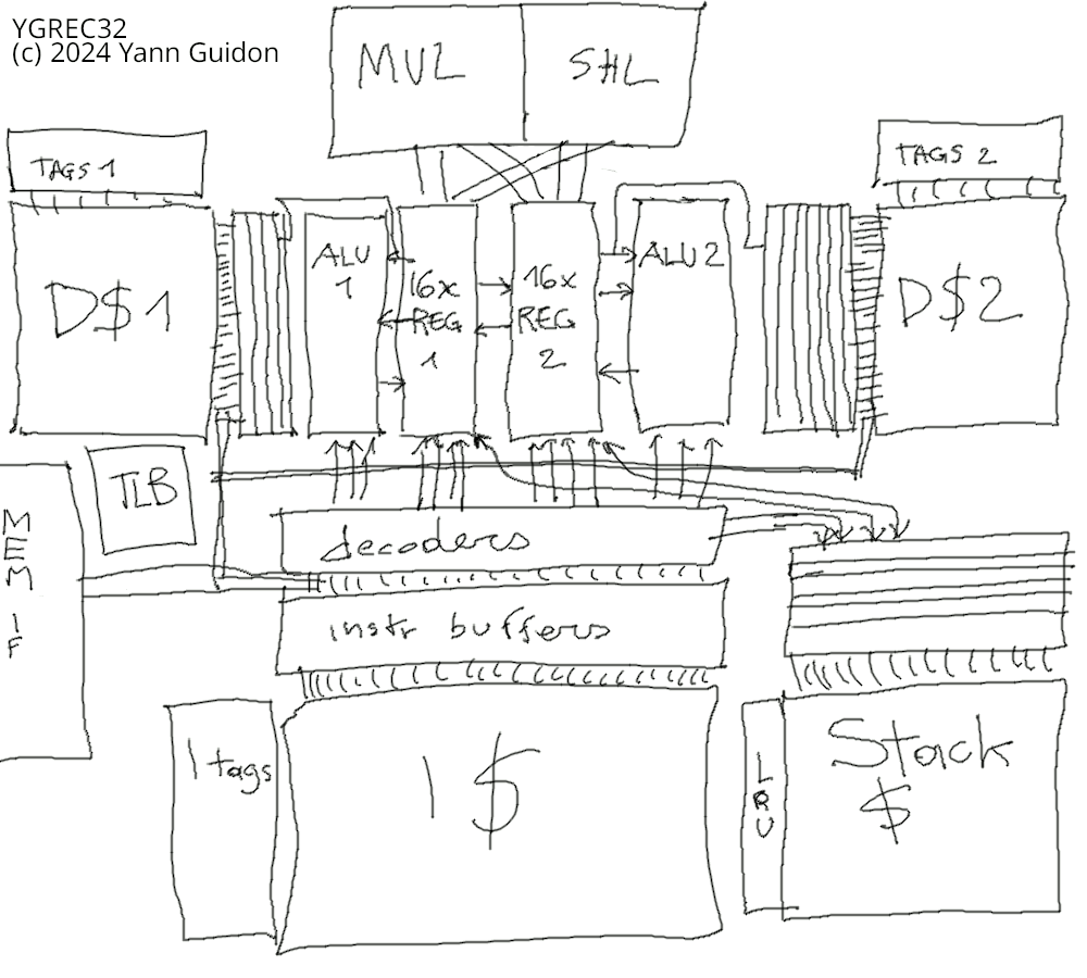
05/10/2024 at 02:34 • 0 commentsThat's about it, you have the rough layout of the YGREC32:
![]()
Sorry for the quick&dirty look, I'll take time later to redraw it better.
It's certainly more complex than the YASEP32 and it looks like a simpler but fatter F-CPU FC0.
There are a number of differentiating features, some inherited from FC0 (don't fire a winning team) and some quite recent, in particular the "globule" approach : a globule is a partial register set associated with a tightly coupled ALU and a data cache block. Copy&paste and you get 32 registers that work fast in parallel, which FC0 couldn't do.
YGREC32 has 2 globules, FC1 will have 4, but a more classic and superpipelined version can be chosen instead of the 2-way superscalar.
Scheduling and hazards are not hard to detect and manage, much simpler than FC0, with a simpler scoreboard and no crossbar. Yay! Most instructions are single-cycle, the more complex ones are either decoupled from the globules (in a separate, multi-cycle unit), or they pair the globules.
A superpipelined version with a unified register set would simplify some aspects and make others harder. Why choose a superscalar configuration, and not a single-issue superpipeline ? In 2-way configuration, a sort of per-pipeline FIFO can decouple execution (for a few cycles) so one globule could continue working while another is held idle by a cache fault (as long as data dependencies are respected). This is much less intrusive to implement than SMT though the advantages are moderate as well. But hey, it's a low hanging fruit so why waste it? And doing this with a single-issue pipeline would almost turn into OOO.
Each globule has a 3R1W register set that is small, fast and coupled to the ALU. More complex operations with more than 1 write operation per cycle (such as barrel shifting, multiplies and divisions) are implemented by coupling both globules.
2 read ports of each register set go directly to the ALU and the memory buffers (L0) that cache the respective data cache blocks. The 3rd read port is used for exchange between the twin globules, and/or accessing the stack.
The pipeline is meant to be short so no branch predictor is needed. Meanwhile, the hardware stack also works as a branch target buffer that locks the instruction cache, so the return addresses or loopback addresses (for example) are immediately available, no guessing or training.
I didn't draw it correctly but the tag fields of the instruction cache and data caches are directly linked to the stack unit, to lock certain lines that are expected to be accessed again soon.The native data format is int32. FP32 could be added later. Byte and half-word access is handled by a dedicated/duplicated I/E unit (insert-extract, not shown).
Aliasing of addresses between the 2 globules should be resolved at the cache line level and checking every write to an address register against other address registers of the other globule. I consider adding a 3rd data cache block with one port for each globule to reduce aliasing costs, for example to handle the data stack.
-o-O-0-O-o- I posted the announcement on Facebook:
Yes I haven't finished all the detailed design of Y8 but what's left is only technical implementation, not logical/conceptual design: I can already write ASM programs for Y8!
OTOH the real goal is to define and design a 64-bit 64-register superscalar processor in the spirit of F-CPU. But that's so ambitious...
F-CPU development switched to a different generation called FC1 which uses some of the techniques developed in the context of Y8 (which is a totally scaled down processor barely suitable for running Snake). Between the two, a huuuge architectural gap. But I need to define many high-level aspects of FC1.
So there, behold a bastardised FC1 with only 32 bits per registers, only 2 globules and 32 registers, but without all the bells and whistles that F-CPU has promised for more than a quarter of century!
Duane Sand shared interesting comments:
It looks like your intent is a dual-issue in-order RISC with a shallow pipeline. Using a design that could scale up to a 4-issue VLIW. The main register file is physically split up between ALU globs, a bit like how later DEC Alphas were implemented. You split up the data cache into 3 or 7 caches that run in parallel, rather than a unified dcache with 3 or 7 r/w ports.
What happens when two or more globs address the same cache line in memory? What happens when a glob writes into a shared cache line? I think programming the globs to use totally disjoint variables and proc frames and heap objects would be challenging and not scale to general purpose computing.
The stack cache would be very complicated, if its stacked values are ever the target of indirect loads and stores. Some stack machines simplify that problem by flushing all stack regs into memory while doing proc calls.
I didn't skim the FC1 notes enough to understand the functional split here between address regs and data-val regs. That part reminds me of CDC 6600 and of Motorola 68000.
I think your goal was for one glob pipeline to remain unblocked and continue computing ahead, when another glob pauses on an innermost-cache miss. How does the ifetch path support that and do the steering? Does the programmer and compiler see all this as a plain sequential processor?
In the FC1 notes, I totally didn't get how the machine helps your goal of capability-based secure computing.
This design reminds me of the Rational R1000 cpu which had two globs. One for executing the program's data calcs and branches. And the second glob for concurrently executing implicit datatype checks. Both globs were driven by a single wide microcode engine. Only the microcoders had to deal with the 2-glob physical nature of the machine.And here are my replies:
Thanks for your thoroughness 😃
The goal of splitting the data caches is many-fold, in particular increasing the number and speed of the individual blocs, since a larger bloc is slower and adding ports makes it worse. This also reduces thrashing (though I'm also working on a LRU system that also provides MRU policy). But also I want to seriously increase cache-reg bandwidth. This last part is partly provided by the L0 lines/buffers between the L1 blocs and the respective "globs".
Aliasing is an old inherent problem, particularly for FC1. the problem is less severe for Y32 there but it's still present. Part of the solution comes from the very mechanic of addressing: the address is not computed during a load/store instruction because it does not exist. The address is explicitly computed and written to an address register and at most 2 results are computed for each cycle, so it's easy to compare the tags of both cache blocks. Eventually, a unified cache tag array could do the magic here.
Another aspect is that the reference for memory coherency is the L0 buffer, not the cache, and these buffers (say 4 or 8 lines per cache block) can communicate faster than when addressing the large array.
I am still examining the split and I consider having a third L1 cache that is shared between the globs for use, indeed, with the data stack frame. So each glob could have 3 memory ports, 2 for the local bloc and 1 to the shared bloc.
There is already a protected control stack that is under active design right now and will be published. Yes it's a bit complicated BUT it resides in its own addressing space, out of reach of the user application so aliasing is absolutely not a concern, and it prevents many common flaws that still make headlines today (iconv flaw, ROP gadgets, stack smashing in general...)
There are no indirect load or stores on the protected stack, or at least not how you might imagine. The stack cache "plays along" with the other stack blocs to "freeze" cache lines associated with its entries, so it acts like a "branch target buffer", among other things. The complexity comes from other parts of the ABI/design though.
---------------------- Duane Sand said: "Some stack machines simplify that problem by flushing all stack regs into memory while doing proc calls."
yg: In this case, it's different : the stack cache is dedicated to certain features only and pushes only a few registers in a very limited number of cases, because the many data cache ports available to the globs make it faster to dump there.
(extra note: Y32 is not a stack machine and no "data" is processed or resides on it)
This is not a general purpose stack and the "frame" is located in the data L1, where the normal registers can access data. However the control of execution flow never leaves the decoding/stack complex and can't be hijacked, in part with techniques like "branch target identification": you can't return to an address that is not a call instruction.
As for FC1, the online notes are still quite vague but you can see some early implementation in the YASEP. Yes there is some CDC6600ness and I am aware of the 68k. My motivation here is that like the CDC machines, memory is slow. Cache is the exception when the worst case happens. You have to load a whole DRAM row in a buffer to start executing the code or use data. So the A/D registers are a sort of window to the buffers (L0). This is not very relevant for old/slower designs but the faster CPU internally split a load or store in two microops anyway. Here, llike the CDC6600 I give an opportunity to statically schedule a "prefetch" before accessing the data itself when the operation takes place.
---------------------- > "I think your goal was for one glob pipeline to remain unblocked and continue computing ahead,"
Yep, I entertain this idea of decoupling the "globs", maybe with a little FIFO that splits the instruction streams after they are demuxed and deemed independent.
A depth of 4 sounds reasonable but it's not a priority, it is an opportunity of enhancement for later. It's still far from the efficiency of a pure OOO core but the price to pay for this small adaptation (8×32 bits) is small and does not change the overall processor structure. This would become a bigger headache for FC1 with its 4 parallel globs, though. But let's focus on making it work before optimising it.
But yes the decoupling keeps a strict coherent instruction flow, so the same binary can work on a single-issue superpipelined core or whatever people want to play with. The only user-visible constraint is the separate control stack (you can't pop or push to the hardware protected stack and mess with it) and the registers are tied to one glob. There is no need to recompile if you update the CPU.Capability-based computing : it's still in its infancy for now, I'm slowly working on it, maybe I'll have a definitive answer in a year 😛
Rational R1000 : you made me discover it less than a week ago so I can't say much. I can say that I have programmed the Pentium to reach 98% of its peak efficiency through extensive manual optimisations, and I collected countless notes on how to do something and not to screw the programmer. I recently found a description of the MIPS R5000 that has some similar features as well. But like the Alpha, the 2 pipelines have a dedicated way for the FP units, limiting the throughput. Y32 and FC1 are more symmetrical and can execute most arithm/mem operation anywhere, except for the jumps and rets that would ideally be in the 2nd slot (for efficiency reasons).
---------------------- Duane Sand "shallow pipeline"
yg: that's spot on!
The BTB indirectly provided by the stack helps absorb some latencies, a one-cycle bubble is considered harmless so a branch predictor is not needed.
Performance is very affected by the memory latencies so there is a strong emphasis on prefetch, hinting, caching "right", splitting address generation and data use...
The philosophy, like in the original FC0, is to squeeze as much performance with a simple and smart design without going OOOe. FC0 used "out of order completion" (a bit like CDC6600) and it was already a warm mess. It is reasonable to consider an in-order core as much easier to implement and to "get working right" faster, then only can we optimise. Y32 is a step in this direction, not the destination---------------------- For a two-issue, two-ALU machine, I think it would be adequate to support just one write-to-dcache operation per cycle. And maybe just one read-or-write to data cache, per cycle. The 2 or more globs do not have to be functionally identical.
Your stack cache is exposing and leveraging the hidden hardware call/return stack that is implemented by branch predictor boxes in all high-perf cpu cores. Nice! Besides holding frame pointers and return branch addresses securely, it could hold the unexecuted portions of code cache lines of recent callers. Maybe giving zero-time returns.
Some secure machines use tag bits on every individual memory word to protect the critical words. Other machines segregate all those critical words into their own segments or pages, protected by segment- or page-level tag bits in the TLB. You are using protection at that segregated level, with separately addressed control frames and data frames. That could be enough. You don't need to have dedicated physical caching of that info too, in a minimal implementation. Sharing the L0 dcache structures would work, maybe augmented by a small buffer.
Most RISC machines use (reg)+immed as their primary addressing mode. This handles C stack frames well and global variables. But it adds an additional pipeline stage. AMD's forgotten AM29000 RISC arch of 1988 had reg-indirect as its only addressing mode. Just like in microengines. This required a separate add-immediate or load-immediate instruction for most loads and stores, but the pipeline was shorter. Another advantage is that the TLB conversion to physical addresses or the he tag probe could maybe be started sooner or done only once.
Controlling when DRAM rows get activated is a very hard problem now, with cpu cores cycling 350 times faster than DRAM. Controlling DRAM row actions from the instruction stream is hopeless. At best, the address registers can be hints to the cache mechanisms. With some kind of simple predictor monitoring successive DRAM cache line requests coming from the outermost cache. Or let the programmer hint this via I/O operations, for raster ops or float pt vectors.
yg:
only one port for cache, shared by the globs ? no way.
This plagued the Pentium for example. There is no benefit to limit the ports, unless you are severely constrained by the silicon area.
Think of saving/restoring the whole register set without a register window...Furthermore Y32 is not a load-store machine, but more like the CDC660.
except that the CDC reserved some registers for writes and other for reads.Y32 has relatively few registers, maybe 16 or 20 GPR, the rest are address and data registers, but they map directly to L0 and they can act as a "register window" if you modify the associated address register.
This is consistent with the purpose of the machine which is not destined for heavy duty computations.There is also a high chance that Y1 would be implemented in a silicon process that is not well exploited, where the bulk of the cache ram array is relatively slow.
The Y32 compromises the GPR space, where others (MIPS, ARM) will cache data from RAM, with a direct window to memory. Change the address of the window, tadah you have your data immediately as a register (unless you cast it or change the format, then the GPR must cache the result).Load/store bandwidth is a critical resource. And with FC1 it will be even more critical because I intend to do even crazier (but the method is not yet well formed enough to give authoritaive replies).
The register-mapped memory practically decouples the core(s) from the memory and can be designed less tightly.
..........
> "The 2 or more globs do not have to be functionally identical."
Of course it's not a hard requirement and there will be slight asymmetries so a pair of consecutive instructions will be able to perform 4R2W operations for example, with each half doing some of the work.However in practice, and for the sake of the compiler writers' sanity, orthogonality and symmetries are very, very much desired. Already the asymmetry due to the split caches creates a memory allocation constraint that is not usual and I don't want to increase the burden.
The principle of the globules is that they are identical, small, simple, tailored for speed, and copy-pastable as required. Each does the minimum, more complex operations are shared across the cluster keep the globules as fast as possible. And of course memory access is vital.
One globule would be able to compute the next address while a data item is also read from the data register. Since the starting address comes from a valid register, the new address with a small displacement only needs to be checked if it exceeds a page boundary, relieving the TLB.
.......
> "Your stack cache is exposing and leveraging the hidden hardware call/return stack that is implemented by branch predictor boxes in all high-perf cpu cores. Nice! Besides holding frame pointers and return branch addresses securely, it could hold the unexecuted portions of code cache lines of recent callers. Maybe giving zero-time returns."
That's exactly the point.
maybe not zero cycle, but significantly close to it.
Behind the curtain it's a bit more messy but I want to keep latency as low as possible, which is compatible with the "minimalist" theme of the group 🙂Branch predictions are hard. A Pentium-like branch predictor is nice but uses real estate, has some quirks, requires training... and the same effort (in penalties) is mostly the same for training and untraining.
I try to leverage other sources of context from the program's structure and the stack is perfect for this as it handles:
* if/switch
* loops
* call/ret
* try/throw
* syscalls
(ideally)Handling the first 3 items is already a significant gain, and I keep the usual conditional branch instructions for the cases where the "structured" version does not work but there will be a penalty.
> " Controlling DRAM row actions from the instruction stream is hopeless. "
yes, but it depends on the application and target.
Initially, the YASEP would run at maybe 10 or 100MHz and steer a SDRAM chip directly. It's a perfect match in this case. That's all that was required of that microcontroller.
In the extreme mismatch cases that you mention, latencies are absorbed by huge renaming files, hundreds of instructions remain in flight... and branch prediction is critical.
I'd rather use 2- or 4-way Simultaneous Multithreading, which is compatible with the Y32 since the globules have a very small number of registers. So extending each globule to 32 or 64 registers would not impede the frequency too much. It remains quite scalable. A monolithic register file would soon become too large and slow the pipeline down (this was an issue with FC0 that the blobules try to address).Realistically, at this moment, I think that I can handle a CPU that runs at about 200MHz FSB. I have matching pipelined SSRAM and the PCB design is still not too hard. 1MB or 2MB SSRAM at 250MHz can be found on eBay, the kinds of chip you can find loitering around an Alpha or R10K CPU. Maybe I can double-clock the core to 400Mhz eventually. This is compatible with a recent FPGA or a cheap fab run on 350nm, if I can't access the 180nm of GloFo or Skywater. All I have to do is make sure I have enough L2 onchip!
So for now I'm not too concerned about extreme RAM delays. There is more important for now, as I have not even defined the instruction set format.
YGREC32
because F-CPU, YASEP and YGREC8 are not enough and I want to get started with the FC1 but it's too ambitious yet.