Close
0%
0%

RPi Pico Video4

A RPI Pico RP2040 board with 4 composite video outputs, 8 inputs and switched power

Similar projects worth following
The Pico Video4 Display is a stand-alone RPi Pico RP2040 board, connected through USB-C.
This board provides up to 4 analog composite video display interfaces with integrated frame buffer memory accessible through SPI. The 4 video outputs are accessible through 1 RCA connector and 1 VGA DB15-HD connector that uses the red, green and blue channels for the composite signal.
The heart of this design is the VLSI VS23S040 chip. PAL and NTSC output formats are supported. Currently 4 resolutions are implemented: NTSC 320x200 or 426x200 with 256 colours and PAL 300x240 or 500x240 with 256 colours. The chip has a 1Mbit framebuffer per channel, unused memory can be used for graphics tiles, which can be copied into the image data by the internal fast memory block move hardware.
A 16 Mbit SPI FLASH memory is available on-board, loaded with a character bitmap, a Amiga Boing Ball demo, and 9 images ready to display.
It has 8 inputs that are voltage compatible to the input voltage; up to 12 V.

  • Operating supply voltage 5.0 V – 12 V
  • Raspberry Pi Pico with 16 Mbit Program Flash memory
  • USB-C connector for 5 V power and communication/programming
  • SWdebug header
  • 4x Composite Video Output
  • Maximum resolution 720x576 in 4 colours
  • Implemented resolutions: NTSC 320x200 or 426x200 with 256 colours and PAL 300x240 or 500x240 with 256 colours
  • Crystal: NTSC 3.579545 MHz or PAL 4.43618 MHz
  • Communication interface: SPI up to 38 MHz
  • Video Frame Buffer: 4x 1 Mbit = 4x 128 KByte
  • Data Flash: 16 Mbit = 2 Mbyte
  • QWIIK I2C connector
  • 8 inputs, high voltage up to input voltage level 5-12 V, with LED indicator
  • 8 dip switches to simulate the inputs
  • LED and 2-pin jumper for status and control
  • Power output, switched and fused with 500mA polyfuse
  • TH prototyping area
  • Size: 85mm x 100mm (3.3" x 3.9")

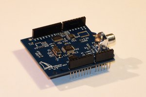
This board is the continuation of my 2 Arduino Shields NTSC/PAL Video Display Shield | Hackaday.io and VGA Shield Wing | Hackaday.io.

ASSY P42-Pico_Video4 rev1.pdf

Assembly drawing

Adobe Portable Document Format - 912.55 kB - 07/21/2024 at 19:08

Preview

SCH P42-Pico_Video4 rev1.pdf

Schematic designed in KiCAD

Adobe Portable Document Format - 1.28 MB - 07/02/2024 at 00:31

Preview

  • 1 × RP2040 RaspberryPi Pico MCU
  • 1 × VS23S040 VLSI 4x video composite video chip
  • 1 × USB-C
  • 1 × RCA connector

  • Meandering traces of (not so intelligent) autorouters

    MagicWolfi11/07/2024 at 01:15 0 comments

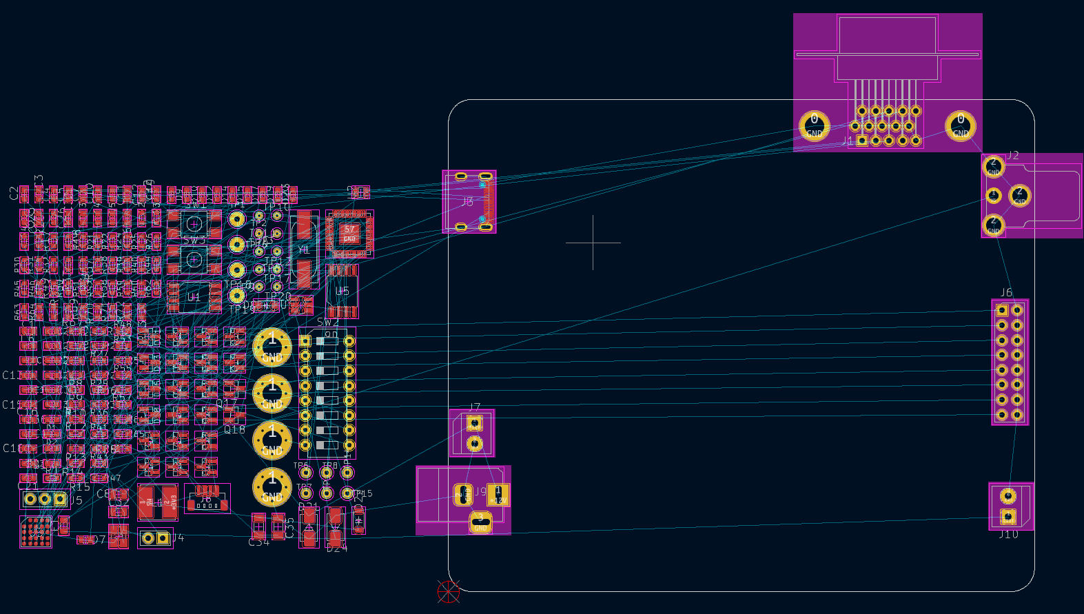
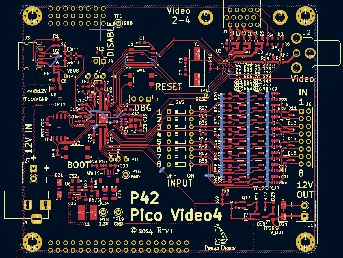
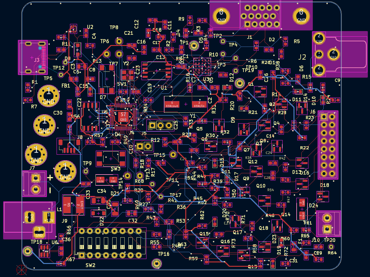
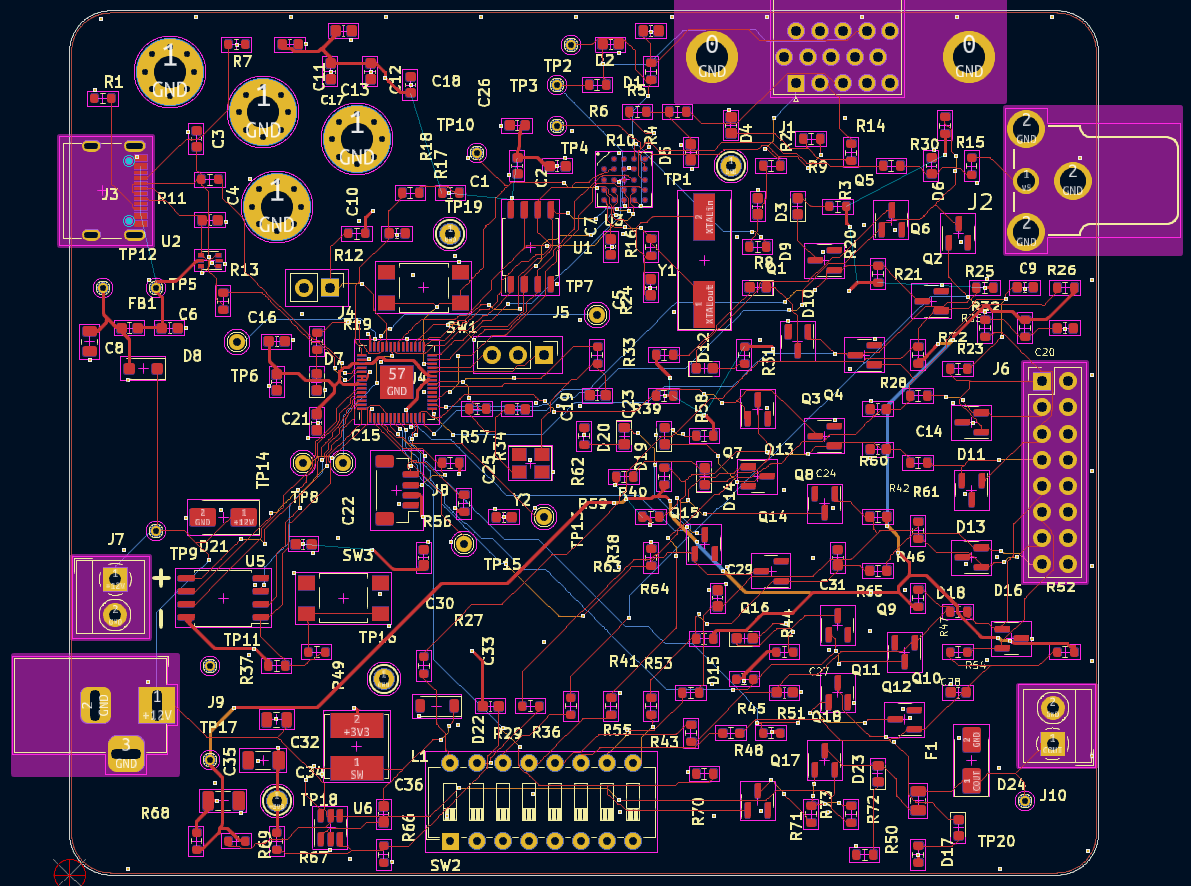
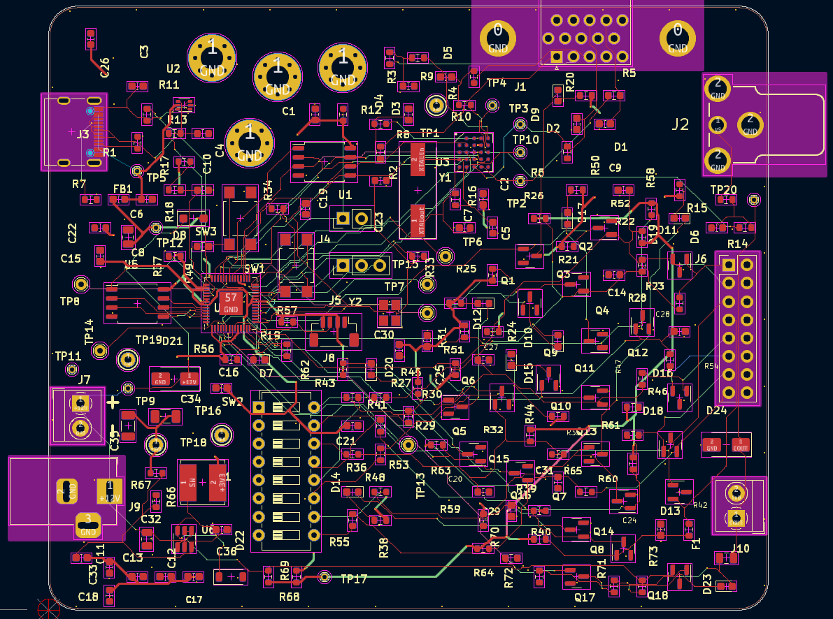
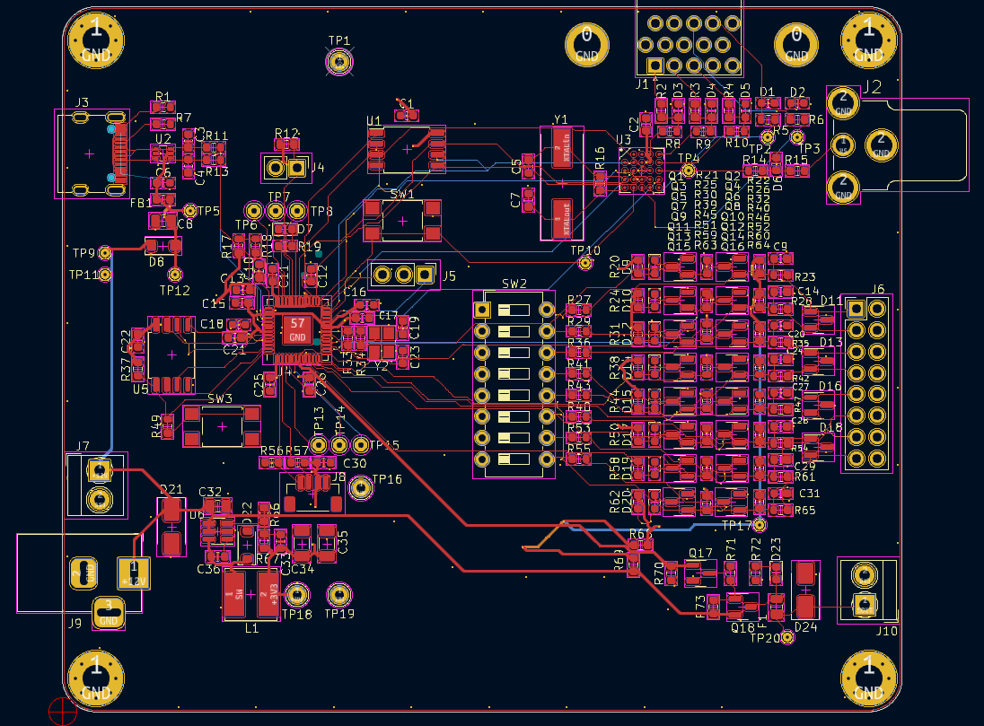
    I am writing the log mostly because I used this project PCB in some exercises of testing a new kid on the autorouter-block.

    Inspired by an interview of the founder of the Quilter autorouter [Sergiy Nestorenko], and just having finished to layout my Pico-Video4 board, I spend some time comparing the results of my efforts to an AI approach.
    My design was not perfectly in their 'sweet spot' but not too complicated either. To give everybody a fair chance I locked the connector positions. Not locking the mounting holes  was an experiment to see if the AI could make sense of those and ended up in some especially funny results. Highly recommended /s.

    I won't comment on the pictures, the results speak for themselves. I disabled the copper pours to give a better visual on the tracks. Quilter did put put GND pours on every outside and inner layer of the design.

    The starting position:

    My final result 2-layer:

    Quilter, fewest layers 2-layer

    Quilter, shortest tracks 4-layer

    Quilter, no constraints 6-layer

    Quilter, routing only with my pre-placement 4-layer

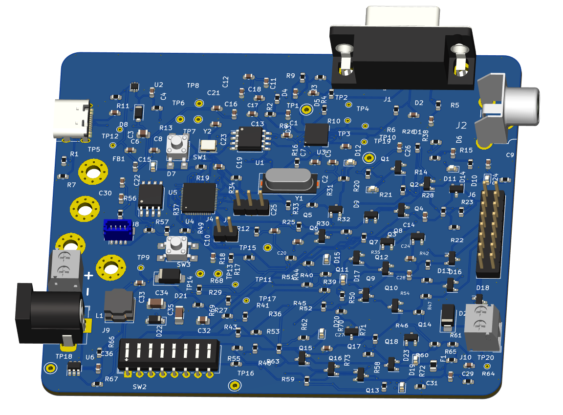
    The layer view just don't do justice to the results, here is a 3D view of the 'fewest layers' board.

    I really would like to have some sponsoring to build one of those boards and see if it works at all. The geometry of the placement alone is beyond me, but looking at functional blocks makes it even worse. 2 examples are a SMPS ( U6 bottom left) and the crystal for the microcontroller Y1-U5 (center upper-left). I really should give it another try without the connectors being locked, maybe that helps.

  • Demo Firmware

    MagicWolfi07/07/2024 at 16:47 0 comments

    3 Demo firmware packages will be available soon:

    1) A memory test that checks for I2C EEPROM, SPI Flash and writes a character set, a Amiga Boing Ball demo and a test image into Flash memory.

    2) A graphics demo that displays the following test routines on all 4 channels:

    • full colour default palette
    • demo image from package 1)
    • Mandelbrot set on channel 0 only
    • colour bars in YUV and RGB colour space
    • all characters from the set written to Flash in package 1)
    • a C-64 inspired start screen
    • the Amiga Boing ball demo, showcasing the block-move (blitter) function of the VS23S040 chip.

    3) A serial port command line application, geared towards storing and displaying BMP images. Some test images are shown in the image gallery for this project.

    Here is a list of implemented commands:

    w[1-8] Write Image into Buffer 1-8
    w0     Write Logo Image into Memory 128x128 px^2
    i[1-8] Colour convert and write Image into Buffer 1-8
    i0     Colour convert and write Logo Image into Memory 128x128 px^2
    s[0-8] Show Image[0-8] on screen
    m[0-8] Show Memory Dump of Image[0-8] 'x':Exit 'anykey':next page
    d[0-9] Delete memory section of Image[0-9]
    c      Clear Screen
    v      Show Version
    ?      This help command

     Images [1..8] are also displayed, when a respective input is set. If one input is active, the power output of the the board is active as well.  

  • Todo list for rev 2

    MagicWolfi07/05/2024 at 01:05 0 comments

    1) Change D11,D13,D16,D18 to common anode ESD diodes LCSC C122858 MMBT15VA
    2) Change R19 and R72 to 10K, to adjust LED brightness 
    3) Move RCD matrix away from J6 to make room for shrouded conn
    4) Change 12V IN label to 5-12V
    5) +12V fill top layer straight line
    6) Change buttons to something more user-friendly
    7) Change R16, R33 to 1MOhm in the Mfr PN field.
    8) Move GPIO15,21,22 testpoints to the top as proper TH testpoints
    9) Make the housing pads of J8 larger to the outside and fix the "QWIIC" spelling error.

    10)Adjust TH rows of VGA connector for low profile version

    11) Fix pin mapping on QWIIC connector J8 (For obvious compatibility reasons you must follow the same pinout: GND / 3.3V / SDA / SCL.)

    12) Add an uSD card slot for a boatload of storage (use SPI, not SPI1)

View all 3 project logs

Enjoy this project?

Share

Discussions

Similar Projects

Does this project spark your interest?

Become a member to follow this project and never miss any updates