-
Video and CPU sharing memory
09/05/2018 at 11:49 • 0 commentsIf the video display and CPU are to share the same RAM, then some way is needed for them to concurrently access it. The video data has to be written out to the screen on a fixed schedule as that pixel will be expected by the display at the correct instant. The CPU can wait for data to be read or written - there is no hard deadline.
The RAM has only a single read/write port and can only do one thing at once and takes a fixed amount of time to do this.
One way to allow the video to not operate on such a fixed schedule is to use a FIFO - the video data is read out of the RAM "whenever possible" into the FIFO. The FIFO then has data extracted from it on a fixed clock whenever a pixel is needed. If data is not added to the FIFO in time then there will be an underrun and the image data will have a temporary corruption.
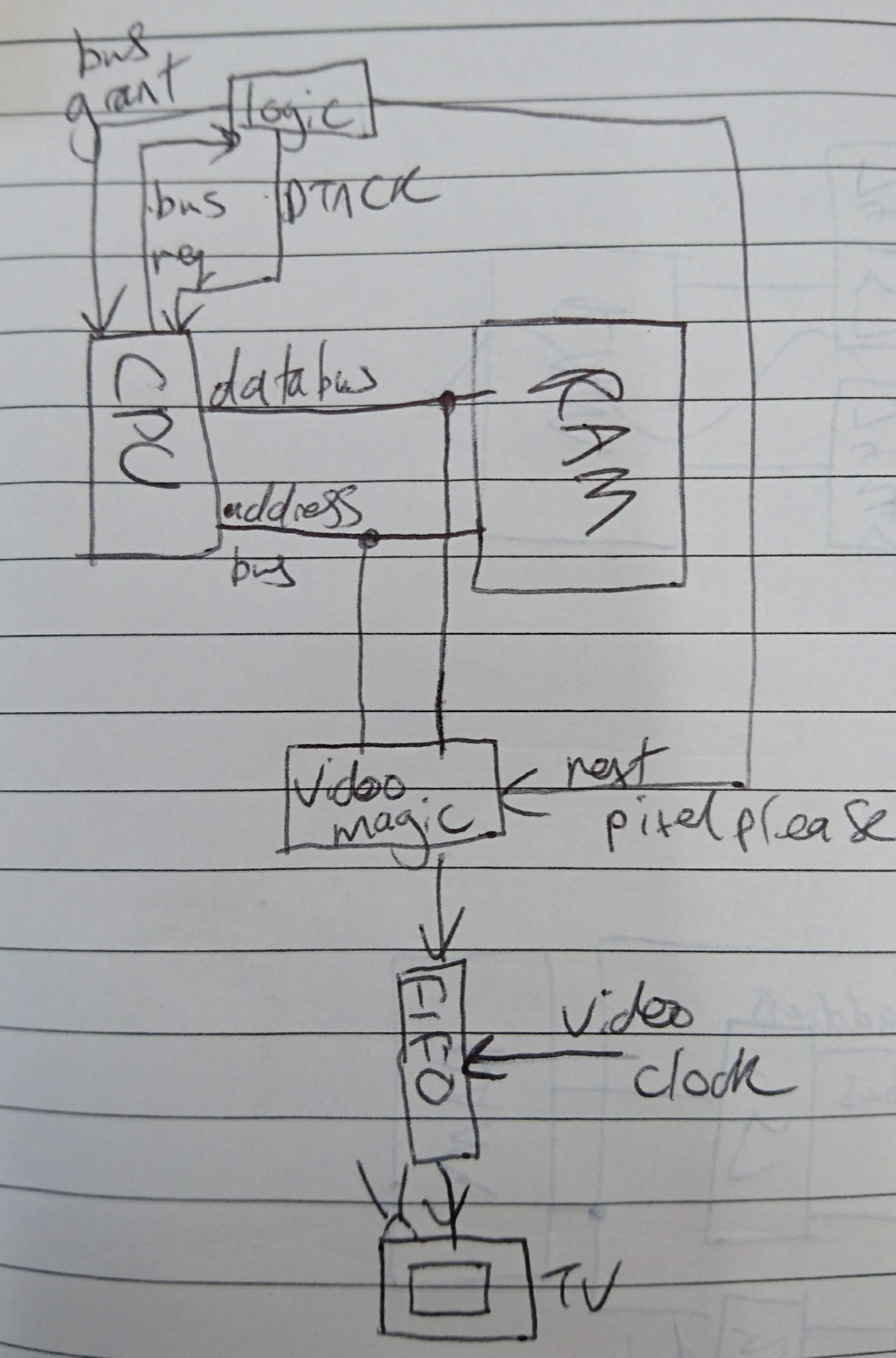
If we get the CPU to relinquish the bus and go to high-impedance whenever we need data, then we can read out a pixel and add it to the FIFO.
The CPU provides a mechanism to arbitrate for the data and address busses via the "bus grant" and "bus request" pins. This takes a certain amount of clock cycles though and gives an unpredictable latency depending on what instruction the CPU is performing. It does require the FIFO though, but doesn't require other circuitry to lock out the bus (as the CPU is doing the high-Z for you).
In retrospect I wish I had looked a bit more into this idea - it's not the way I went in the end.
The route that I chose instead was to not use a FIFO and allow video to be directly scanned out from the RAM at the exact time required. This then meant using a lock on the bus and delaying DTACK until the lock was lifted and the CPU's data dealt with.
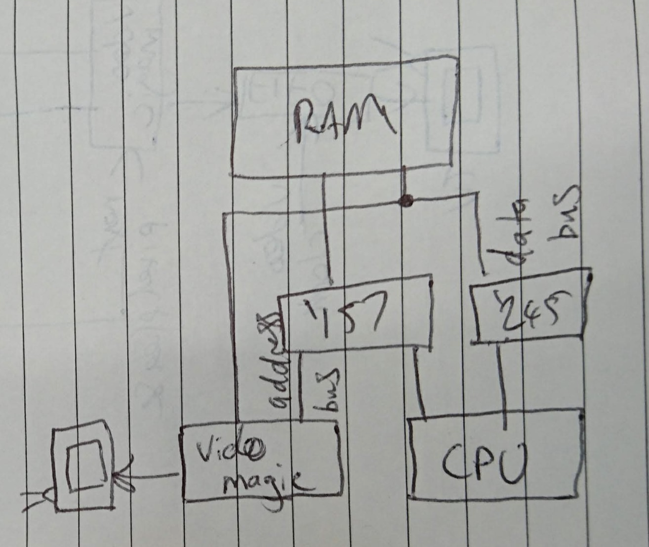
There are two elements to this lock: the data bus and the address bus.
The data bus
If you consider the data bus, the CPU both reads and writes data to the RAM. The video hardware only reads from the RAM.
If we use a 74'245 octal bus transceiver between the CPU's data bus and the RAM's data bus, we can use it's high-Z feature to disable the CPU's data at any point. If the CPU is driving the bus (ie it wants to write to memory) we can simply disable it via the '245's "output enable" (OE) pin.
This allows the video hardware to access the RAM at any time. Just deassert the OE pin on the '245.
When the CPU is granted access to the data bus the OE pin is asserted and 'direction' (DIR) is controlled with the CPU's R/W pin. If it wants to read from the RAM DIR is set such that the signal is driven from the RAM side to the CPU side. If it wants to write the signal is driven from the CPU side to the RAM side.
A single '245 controls eight bits at a time. Our 68008 has an eight-bit data bus so we only need one. Happy days. The video hardware only ever reads, so no additional hardware is needed - it is connected directly to the RAM's data bus and only latches data when we want it to (so if it 'sees' CPU data there's no worry).
The address bus
Both the mystery video hardware and CPU both drive the address bus in order to select which byte they wish to access (and they will both do it at the same time). So depending on which has precedence, we need to pass just one of these addresses (and the corresponding read/write signal) to the RAM. We will do this with a 2-to-1 multiplexer. Given two inputs we will select one of them to be the output, based on some other signal.
The RAM is 512 kB wide - 19 bits - and these '157s select four bits at a time so we will need five of them. That leaves a pin free to also pass through our read/write signal.
Those '157s will then use a common signal from the control logic to either select the address from the CPU (and its R/W pin) or the address from the video hardware (and its fixed 'read' signal).
The logic
The logic within the system will need to select the video hardware on a fixed timer, and then choose to lock out the data bus, to switch the address bus and finally to control DTACK.
A key part of the "video hardware" is just a binary counter which holds the address (in bytes) of the active region of the screen. As this increments it points to a different pixel/group of pixels within the framebuffer, stored in the RAM. Every time the video hardware is selected by the control logic, the counters count up by one.
-
Wow so it has been ages
09/05/2018 at 10:33 • 0 commentsWhen I originally made this blog, I was writing retrospectively - adding logs a few months after I did some work. At some point I got a bit behind...and the rest is history! In the mean time hundreds of hours of work have been done and lots has been learnt though success and failure.
Time to fill you guys in!
-
What video interface?
07/16/2017 at 18:25 • 0 commentsSo having decided to add video, the next question would be: what kind of of output would be necessary to connect to the display? Again there are some choices depending on how much you want to do yourself and how much you want to hand off to a pre-made chip. Making this I wanted to learn as much as possible and do it all myself so I think this really boiled down to three options.
- Composite video. One signal wire which has the both control values and the actual video data modulated together. Interlaced. Colour is problematic. Upper resolution limit of 10 Mpix/s. One scanline required every ~64 us (512 clock cycles at 8 MHz). Input not present on my TV. Similar restrictions apply to S-Video.
- YPbPr component video. Three signal wires, with control plus signal combined with the Y signal. Complex encoding. Good image possible; interlace not required.
- VGA. Not present on most TVs. Good picture quality, high resolutions possible. Easy encoding. Lots of signal pins. 640x480 minimum standard nearer 20 Mpix/s. One scanline in ~32 us.
I chose composite, but if I were to do it again I'm not sure I would make that choice. I have a composite to HDMI adaptor so that removes a lot of complexity (plus I only need to make the signal work with that one device). Also the Arduino tv-out library was an excellent starter for providing the carrier signal. Finally a number of other choices meant higher resolution and bit depth/colour were not relevant to me. Getting composite to work has been challenging enough!
Looking a bit more in depth at these specs, YPbPr would be doable. You would just require the CPU to write data encoded in that fashion directly into memory. I'm not sure what circuit I would use to turn RGB into YPbPr!
VGA is probably too fast for this CPU, assuming synchronised clocks. Or if a double-rate clock was used, the memory would need to be considerably faster. Though to be fair the pixel rate is flexible, but the vertical resolution is not. If the pixel clock were halved we could have 320x480. Or one quarter, it could be 160x480, but these strange rectangular pixels would not be very nice.
Composite it is.
-
Adding video - decisions
07/16/2017 at 10:17 • 0 commentsIt's time to add video-out to the circuit...but how! There are a lot of different options but - considering I've never done anything like this before - the simpler the better.
There are three main choices:
- Have a framebuffer that the CPU can write into, which gets scanned out to the display by another piece of hardware. This is a bitmap, held in memory where each location's value represents the colour or luminosity for a particular pixel on the display.
- Pros: complex images can be drawn with ease as the CPU can build up a picture independently of the display hardware. The CPU can take as long as it likes.
- Cons: requires memory. If it's from the main pool of memory then a way needs to be made to arbitrate CPU/scan-out access. If it's an extra pool of memory, how does the CPU write into it?
- Have a one-line virtual framebuffer, like the Atari 2600. This design does not require any memory (or no more than one pixel's memory) and the CPU directly writes each pixel's value from registers straight to the TV.
- Pros: requires no memory, simple circuit.
- Cons: requires all the CPU time just to make the picture. Free time only available in the hblank or vblank. Hard to make complex images due to the limited time per pixel.
- Have an abstract command-based image generator. For example, you can buy LCD panels which have a simple GPU included. You write the "draw pixel at" or "draw circle at" commands to this GPU and it gets on and does it. This GPU manages the connection to the LCD itself.
- Pros: requires no memory (in our circuit), simple circuit, complex images possible, high colour and high resolution possible. No need to worry about the actual video interface.
- Cons: low performance...unless you just want to draw loads of lines and circles on the screen. Less fun - nothing to learn!
So I have decided to go with #1. Having a framebuffer. Lots of stuff to learn, the most flexibility and the most CPU time free. We are trying to make a simple games console so getting useful graphics out onto a TV is a must!
Next time: more decisions.
- Have a framebuffer that the CPU can write into, which gets scanned out to the display by another piece of hardware. This is a bitmap, held in memory where each location's value represents the colour or luminosity for a particular pixel on the display.
-
Some pictures
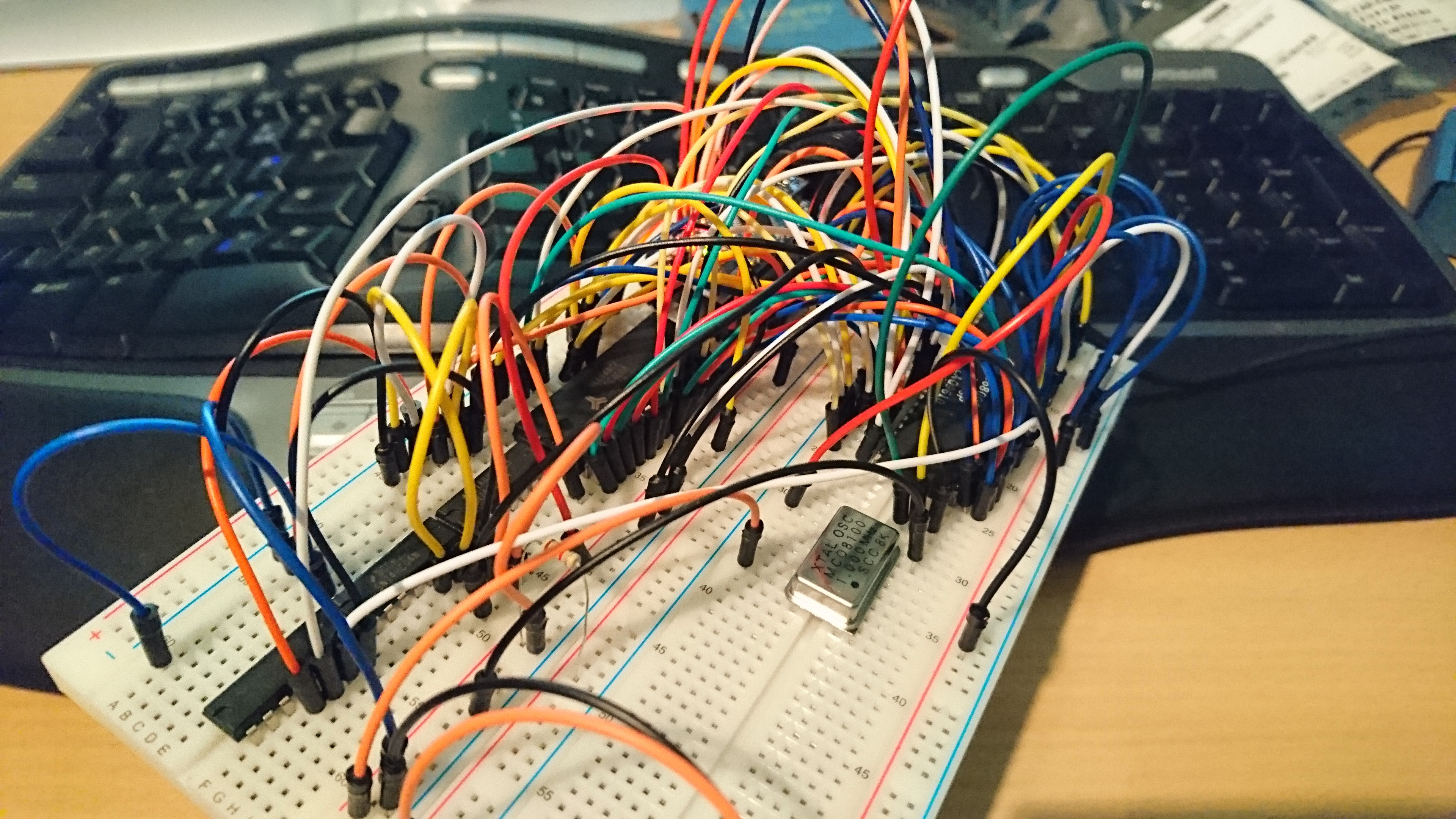
07/16/2017 at 09:30 • 0 commentsAssuming everything has gone to plan, and you've wired up the circuit as described, you're left with something looking like this!
Along the top row: three 74-series logic gates performing the address decoding, the static RAM and then the Arduino.
Along the bottom row: the quartz crystal oscillator and CPU. Also includes a dreadful reset circuit!
![]()
![]()
Here's a video of it in motion so you can see the structure.
-
Address decoding
05/17/2017 at 22:09 • 0 commentsTwo posts ago our CPU was demonstrated connected to an Arduino to provided memory-mapped I/O. This MMIO space could hold code, other board-level I/O functions or perform functions on the host PC. The 'memory' area of this MMIO space was slow - each access had to be interpretted by code running on the Arduino.
In the next post the Arduino was taken away and replaced with memory that went as fast as the bus could drive it! But it had no I/O and no code to run on it.
Let's combine the two. This is pretty easy. To recap the signals required for each device. The changes we need to make are highlighted in bold.
SRAM
- write-enable (WE) is connected directly to the CPU's R/W signal
- output-enable (OE) is tied low
- chip-enable (CE) was tied to the CPU's (address strobe) AS signal, to activate the read/write operation when all the inputs are ready. The CPU's AS signal will assert regardless of the address chosen. We need to restrict this CE signal to be only when the addresses we are interested in are in use
- the 8-bit data bus is connected directly to both the CPU and SRAM. When the CE is not asserted the RAM's inputs will go into a high impedance state, allowing other devices on the same bus to drive a signal.
- the 19-bit RAM address bus is connected to the CPU's A0-A18 address bus, continuing to leave A19 unused by the RAM.
- the CPU has its DTACK signal grounded when the RAM is in use, to indicate no wait states. The RAM is fast enough to satisfy the CPU.
Arduino
- the CPU's R/W signal and a number of address lines are connected to a 74'165 shift parallel-in serial-out shift register. When the Arduino wants to read one of these signals, it captures them all in the register then shifts them in one at a time.
- the 8-bit data bus is connected directly to eight of the Arduino's digital data pins. When the Arduino is not in use, these pins are in a high impedance state allowing another device to command the data bus.
- the Arduino's interrupt pin was tied to the CPU's AS signal, to activate the read/write operation when all the inputs are ready. The CPU's AS signal will assert regardless of the address chosen. We need to restrict this signal to be only when the addresses we are interested in are in use
- when the Arduino is in use, the CPU has its DTACK signal connected to an output from the Arduino. It holds it high until the operation is processes, then grounds it for one clock cycle.
Address decoding
So the set-up of two devices is pretty similar. We really only need to do two things - send AS to the right place and receive DTACK from the right place. This place will depend on which address is on the address bus.
In the previous post, as only A0-A18 were connected to the RAM and A19 was left free this turned our 1 MB address space into two 512 KB mirrors of the same RAM. If for instance we only triggered the RAM's chip enable with AS when A19 was low - ie the low 512 KB of the address space - the upper 512 KB could be used for something else. Or vice versa - if the AS signal triggered CE when A19=1 then the 512 KB RAM would appear in the top 512 KB of the address space and the bottom 512 KB would be undefined. There would be no data on the bus and the CPU would read junk.
The same thing applies to the Arduino. Suppose on our shift register we shift in the CPU R/W signal and eight bits of address (A0-A7), if the Arduino interrupt was triggered on every AS then the Arduino address space would mirror every 256 bytes from address zero to the top address: 1 MB. If this signal was only triggered when A19=0 then the Arduino MMIO space would only exist from address zero to the middle of the address space - 512 KB in. The top 512 KB would be undefined.
With a tiny bit of logic we can make ourselves some address decoding. Let's map the Arduino into 256 byte mirrors in the bottom 512 KB and the 512 KB SRAM into the top 512 KB.
Here's a truth table for the chip selects. Remember that AS and the two chip enables are active low.
CPU /AS CPU A19 SRAM /CE Arduino /interrupt 0 0 1 0 0 1 0 1 1 0 1 1 1 1 1 1 Using this solver we can make ourselves some logical equation for this.
and a truth table for the /DTACK signal that goes to the CPU. Also active low.
CPU A19 Arduino /DTACK CPU DTACK 0 0 0 0 1 1 1 0 0 1 1 0 /DTACK = !A19 && /ARDUINO_DTACK
Adding some gates
In order to implement our three equations we will need some logic gates. We could just use NAND or NOR gates but perhaps let's just use the logical operations described by the equations above: NOT, OR and AND.
For NOT I'm going to use a 74'04 - six NOT gates in one package.
For AND I'm going to use a 74'08 - four two-input AND gates
For OR I'm going to use a 74'32 - four two-input OR gates.So far I've been using the "HC" variants of these chips. Compatible with TTL logic, can use a ~5V power supply and reasonably fast switching times. Mine are all from Texas Instruments.
Schematics
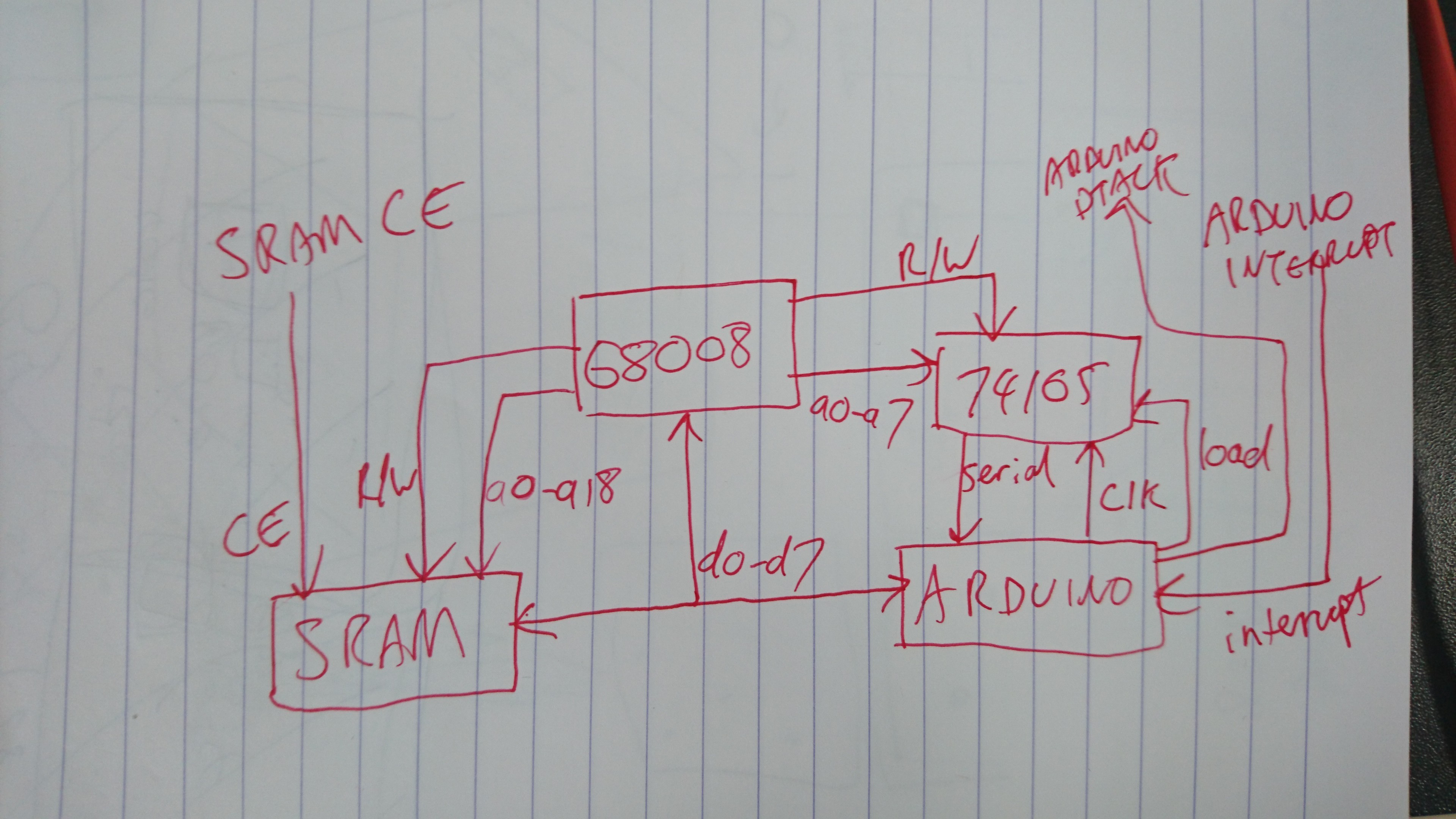
Wire this up. This is the CPU, SRAM and Arduino connection (along with the Arduino's shift register).
![]()
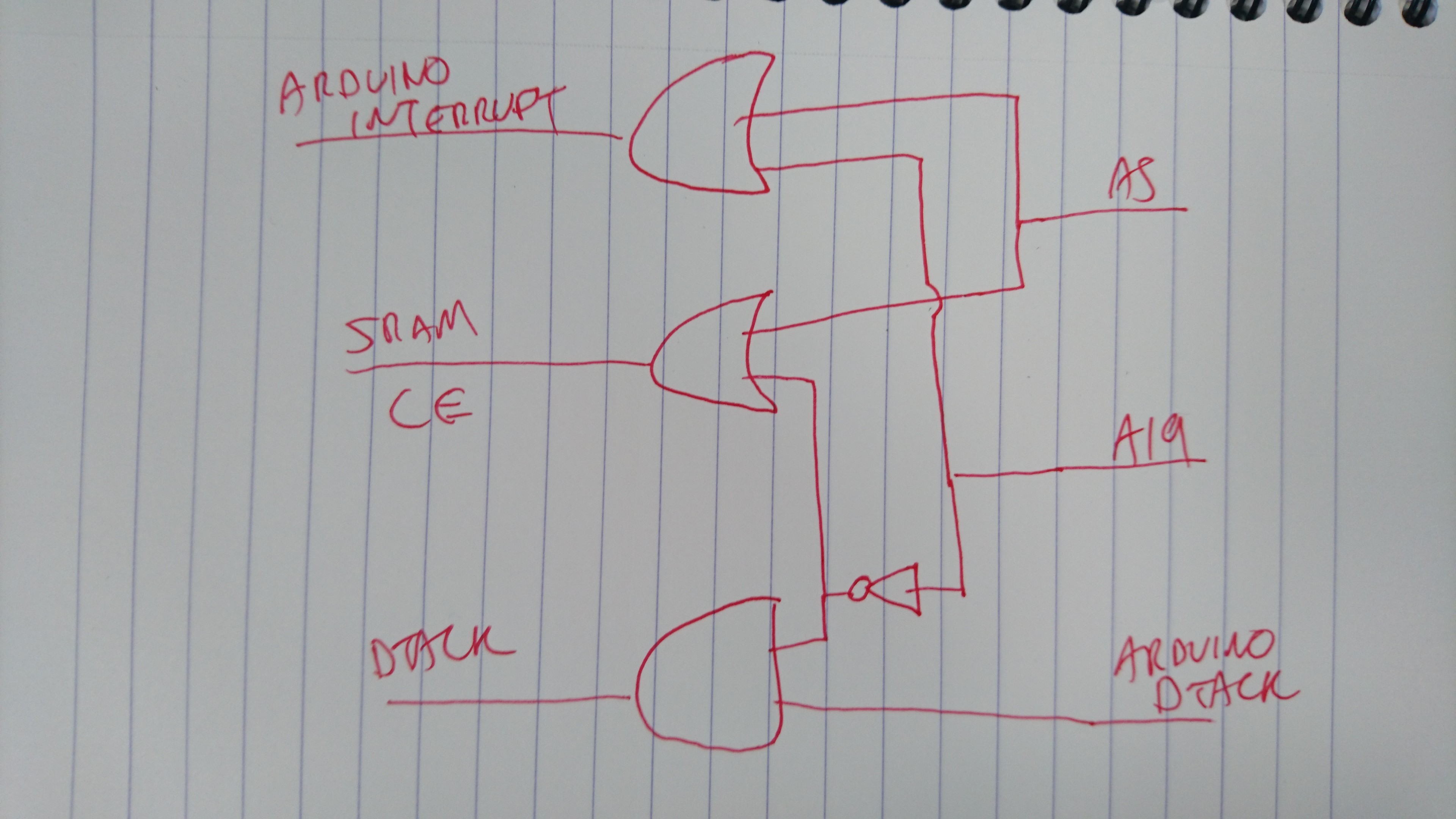
And here's the logic to wire up too. This implements the three equations described above.
![]()
Conclusion
At this point you have a CPU with 512 KB of fast working memory, in addition to an Arduino which can perform any I/O that you want. It can also supply code - replacing a ROM or other file store. The address space looks like this:
- 0x00000-0x000FF - the Arduino MMIO area
- mirrors of this region up to 0x80000
- 0x80000-0xFFFFF - 512 KB of zero wait state static RAM
At this point some may notice I have not described how to reset the circuit...to do this reliably is more complex than you might imagine but that will be for another day!
-
Adding RAM
03/13/2017 at 13:34 • 0 commentsThe last log entry showed a CPU connected to an Arduino, where the Arduino would act as both RAM and I/O, all running via a memory-mapped I/O interface. The address bus was completely connected to the Arduino's inputs. The software running on the microcontroller would then decode the address bus to figure out the intent of the load/store operation. This is great because it allows us to do anything we want from an I/O perspective but directing all traditional memory load/store operations through that route is slow - each bus cycle would take hundreds of 68k cycles.
So let's add a real RAM chip to our system. Parallel static RAMs - the type used here - typically have a simple pin interface. Parallel ROMs are similar too.
- read/write - do we want to read from the RAM or write to it? If write it consumes the data on the data bus; if read then it pushes data onto the data bus.
- chip select - this enables the chip. If enabled then the data bus works as described above. If the chip select is disabled the data bus typically goes into a high impedance state and allows the device to be effectively ignored in the circuit.
- address bus - the linear word address to be read or written
- data bus - pushed by the CPU if a write, pushed by the RAM if a read, high-Z if the chip is disabled
- some sort of 'ok, go' pin - for a read this says "the address set is valid, please now read out that address" or for a write "the address set is valid and the data to write has been loaded onto the data bus - now do the write".
- there is typically no acknowledgement pin to say the action has been performed
RAMs are organised into words and the address bus selects which word is read out on the data bus. The data bus has the same width as the word size. As the 68008 has an 8-bit data bus I'm going to use a RAM with an 8-bit word size. The address bus has the same width as the number of words (in binary bits).
Picking a RAM
I'm going to use an Alliance AS6C4008-55PCN. This is a 5v DIP static RAM with a word size of 8 bits and has 512k words...ie this is a 512 kilobyte RAM. Remember that the 68008 has a 1 megabyte address space - it can't trivially address larger than 1 MB without resorting to funny tricks, so this means the RAM can take up to half of my address space.
This part has a ~55 ns max read cycle. This means that once the "ok, go" pin is asserted the operation will complete in ~55 ns. We're getting ahead of ourselves here a bit but this is fast enough for this CPU at the clock speeds we want to run at (at 4 MHz each clock cycle is 250 ns long and it takes four clock cycles to do a whole bus cycle...of which the RAM has roughly two clock cycles to do its thing. So ~9x more time than we require)
Connecting the RAM
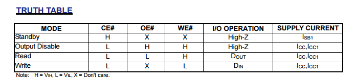
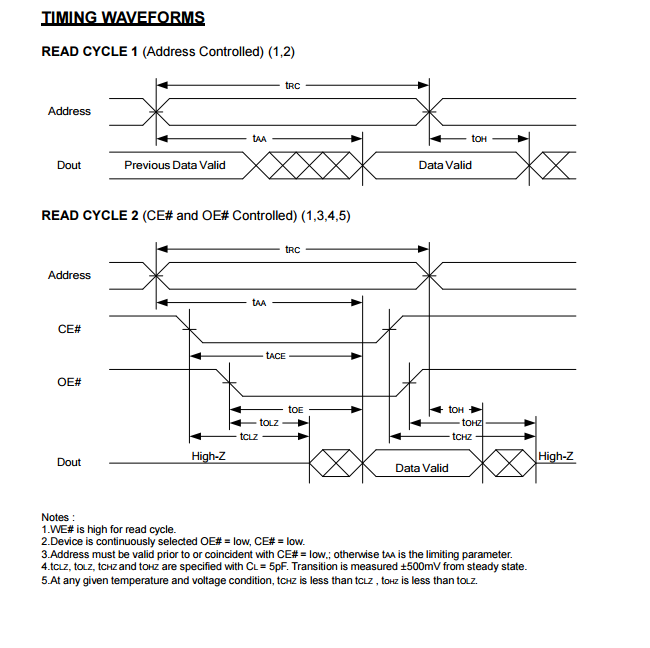
This RAM has three interesting control signals: chip enable (/CE), output enable (/OE) and write enable (/WE). Here's the truth table and the waveform timing diagram.
![]()
![]()
If we only want to connect the RAM directly to the CPU then this is easy.
- The RAM's /WE is connected straight to the CPU's R/W signal. R/W is high for read, low for write which maps directly to the Dout and Din behaviour shown above.
- The /OE is tied low
- /CE is connected to the CPU's /AS. When /AS is low, the address on the address bus is valid. 55ns after /CE is changed the RAM will hold the data on the data bus (and will continue to do so as long as nothing changes). The CPU will latch the data from the data bus at the end of its bus cycle and then negate /AS once it has done this. The write waveform works in a similar fashion.
- we connect the 8-bit RAM data bus directly to the CPU's 8-bit data bus.
- we connect the 19-bit RAM address bus directly to the CPU's A0-A18 address bus. This leaves A19 floating.
- notice the waveform is asynchronous - there is no clock driving any of this stuff.
As we have no other device in the system - it's just the RAM and CPU, and no Arduino - and the RAM has an access time faster than what the CPU requires, we can just tie /DTACK to ground, constantly asserting the signal. This will mean that when that the CPU will never insert any wait states for a memory operation. As mentioned earlier, The CPU gives a ~2 clock cycle window for the memory to do its thing and at 4 MHz that's about 500 ns. Therefore if the RAM were ~9x slower we would need to introduce wait states. So keeping /DTACK asserted is good enough for now.
The memory map
The CPU has a 1 MB address space and memory operations present the address associated with a bus transfer onto the 20 pins of the address bus. As we have not wired the top pin to anything it is ignored by the system - reading/writing to address '1' will present the same address to the RAM as address '524289' (that's 10000000000000000001 in binary). Reading from any address 0<= addr <524288 will return the same value as 524288<= addr < 1048576.
We have mapped the 512 KB RAM block into two locations in our 1 MB address space - the low 512 KB and then the high 512 KB. To be explicit,
- 0x0 - 0x7ffff
- 0x80000 - 0xfffff
What next?
So our CPU has RAM, and RAM as fast as it can run. But when we power on the system the contents of that RAM is undefined. We have no program to run and there's also no I/O (so why even bother run the program?). When the CPU was connected to the Arduino we had all of those thing (but slow RAM). Next time we need to connect all three together somehow.
-
Making a basic system from a CPU and an Arduino
02/23/2017 at 22:22 • 0 commentsSo you've done your free-runner, and you know your £2 CPU from ebay is not a brick. If you need a flashing LED in your home you now what to do. But now let's get busy programming this thing!
A basic system needs compiled code to execute, some sort of I/O and a place to store the temporary data - RAM. If you remember from before, the CPU presents a very generic address/data bus to the outside world. This is its only real means of communicating; there are no I/O ports. All I/O needs to be memory mapped. The bus that comes out does not have any integrated logic for driving DRAM or more complex memories. It just says the address to read...now please give me data. If you want more complex things attached to the bus (like DRAM) you've got to manage that with external component.
A bus cycle
The bus is really simple and requires minimal effort to do anything with it. There are discreet pins for address and data; pin functions are not multiplexed. There are really only three control signals:
- /AS - address strobe. This says "the CPU has placed a valid on the address bus and I am waiting for data". It is active low (hence the slash)
- R/W - read/write. This selects between the two bus modes: read or write. If read, the data bus is configured to receive a signal from an outside source. If write, the CPU places data on the bus ready for an external device to receive. 'R' is active high, 'W' is active low.
- /DTACK - data transfer acknowledge. This is controlled by an external device to say the bus operation has completed. If it was a read from the CPU's point of view, the external device will assert /DTACK once data has been placed on the address bus. If it's a write, the external device will assert /DTACK once the data has been taken from the bus and the operation completed. /DTACK is active low.
The bus take at least four CPU clock cycles to complete one bus transfer - read or write. Each clock cycle is broken into two half-cycles. This means there are eight stage to a bus cycle.
For a read,
- R/W is asserted
- the address is written to the address bus
- /AS is asserted
- (no change)
- the CPU waits for /DTACK to be asserted. If it is not asserted, the CPU will insert whole clock cycles until it is asserted.
- (no change)
- data is read from the data bus into the CPU. Remember - the external device will have asserted /DTACK after it has placed data on the bus!
- this read data is latched, and /AS is negated
A write works in a similar fashion:
- R/W is asserted
- the address is set
- R/W is negated
- data is written on the bus
- the CPU waits for /DTACK...inserting whole clock cycles if not received in this half-cycle
- (no change)
- (no change)
- /AS is negated, R/W is asserted
A memory-mapped Arduino
What we will ultimately do is construct a system with RAM, ROM and I/O - where all I/O is provided by an Arduino. However as mentioned, all I/O is done via memory-mapped I/O. We may as well temporarily get the Arduino to also become ROM and RAM!
We can connect the address and data busses to the pins of our Arduino, in addition to the control signals. The Arduino can listen for /AS, then decode the address, read the data from the bus/write data to the bus, and then assert /DTACK. We can have a small byte array declared in the Arduino and this can represent the 'RAM' address space. The address decoded from the bus can just index into this array. Code and data can be stored in this array.
Here's some pseudocode from what we'll do on the Arduino:
void setup(void)
{
    //wait for the /AS
    attachInterrupt(AS_PIN, &address_strobe);
    write(DTACK, HIGH);
}
//////////////
//our megabyte address space
unsigned char memory_array[1048576];
//////////////
void address_strobe(void)
{
    //read the R/W signal
    bool rw = read(RW_PIN);

    //read the address bus
    unsigned int addr = 0;
    for (int count = 0; count < 20; count++)
         addr |= (read(ADDR_PIN + count) << count);

    if (rw)
    {
         unsigned char data = memory_array[addr & 1048575];
         for (int count = 0; count < 8; count++)
                write(DATA_PIN + count, data & (1 << count);
    }
    else
    {
         unsigned char data = 0;
         for (int count = 0; count < 8; count++)
                data |= (read(DATA_PIN + count) << count);
         memory_array[addr & 1048575] = data;
    }

    //tell the 68k the transfer is ready
    write(DTACK, LOW);
    //wait a few clock cycles
    write(DTACK, HIGH);
}
The amount of time the Arduino will take to do one of these transactions is high - there are a lot of instructions here, and even though it runs at a higher clock speed than the 68k, /DTACK will be high for some time. The 68k will just insert wait states until DTACK is low.
Not enough pins
In the above pseudocode we need at least eight pins for the data bus (used as both input or output), one input pin for /AS, one input pin for R/W, one output pin for DTACK and twenty input pins for the address bus. I'm using an Arduino nano and it does not nearly have enough pins for this!
So we can simplify what we need to get some pins back. We must have the eight data bus pins as they are bidirectional. We must have the /AS, as we use it to trigger an interrupt. We need control over the assertion time of /DTACK. The address bus and R/W are only ever inputs. We can replace these pins with a 74'165 shift register (or three). These integrated circuits allow us to change these parallel signals into a serial one. '165 chips can be chained together so we only need enough circuitry to drive one of them. The problem with doing this is speed - we're changing our parallel bus into a serial one. The more bits we wish to read, the longer it will take.
Driving a '165 chain requires a clock signal, a shift/load signal and a data output signal. To load the register with your parallel signal you simply negate the shift/load signal and then re-assert it. The data is now latched internally. To read the data out one bit at a time you assert and negate the clock signal once for every bit in the register. Each bit will then come out of the data output signal.
This allows us to turn our 21 pins of address and R/W into three pins: clock, shift/load, data. We update our pseudocode accordingly:
    write(SH_LD, LOW);
    //delay
    write(SH_LD, HIGH);
    //data is now latched in the register

    bool rw = read(DATA_PIN);

    unsigned int addr = 0;
    for (int count = 0; count < 20; count++)
    {
         //select the next bit
         write(CLK, LOW);
         //delay
         write(CLK, HIGH);
         addr |= (read(DATA_PIN << count);
    }
(this assumes the R/W signal is connected to the parallel input as the first signal, with each address bit connected sequentially)Adding hypercalls
Our Arduino now acts as RAM - the CPU can read and write data to it. The Arduino simply acts as a slow, dumb memory. However the Arduino is connected to the host PC - it also has other spare pins we can do interesting things with. We can add memory-mapped I/O to the system easily by simply re-defining certain addresses within the memory space to do special things.
eg,
    if (rw)
    {
         unsigned char data = 0;
         //an arbitrary address
         if (addr == 0x1000)
                data = read_host_keyboard();     //and arbitrary function
         else
                data = memory_array[addr & 1048575];
         for (int count = 0; count < 8; count++)
                write(DATA_PIN + count, data & (1 << count);
    }
    else
    {
         unsigned char data = 0;
         for (int count = 0; count < 8; count++)
                data |= (read(DATA_PIN + count) << count);
         if (addr == 0x1000)
                write_host_console(data);
         else
                memory_array[addr & 1048575] = data;
    }
The 68k can now communicate with the outside world. By constructing a simple MMIO command protocol we can command the Arduino to do any function we like.
Next time we'll add real RAM...
-
Free-running!
02/07/2017 at 21:39 • 0 commentsThis project started with me seeing an MC 68000 on a breadboard blinking an LED. It seems this is a rite of passage for 68k builds. Although a little bit of a challenge at the time, it's a great way of getting to know your way around the physical package of your CPU. It's also a great way to check the chip and your power supply work. That LED and your stopwatch are your only debugging info!
It really is worth reading the manual rather than blindly copying a circuit off the 'net - I've provided mine to be consistent. Each site has a slight variation (especially for reset) and it's important to know what you are wiring up and why.
![]() (By Konstantin Lanzet (with permission) - CPU collection Konstantin Lanzet, CC BY-SA 3.0, https://commons.wikimedia.org/w/index.php?curid=4774280)
(By Konstantin Lanzet (with permission) - CPU collection Konstantin Lanzet, CC BY-SA 3.0, https://commons.wikimedia.org/w/index.php?curid=4774280)The CPU provides both input and output signals, and some which can go both ways. Unlike a modern SoC, there is very little on-chip. You've got to connect everything to it yourself which makes things fun. The main signals include,
- 20 bits worth of address bus (output)
- 8 bits worth of data bus (bidirectional)
- a mixture of in/out bus control signals for operating this bus
- a mixture of peripheral control signals for legacy and more generic peripherals
- interrupt triggering signals (input)
- reset, halt signals (bidirectional)
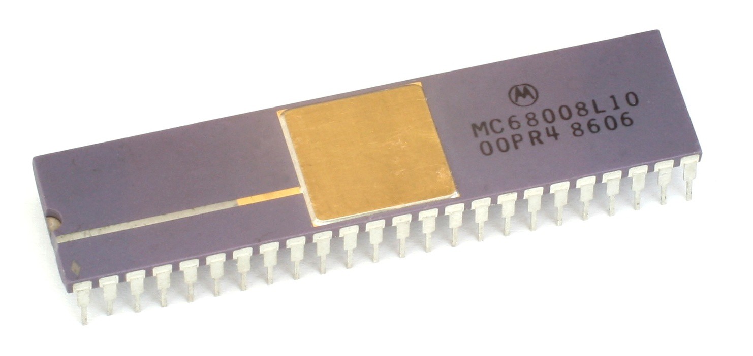
This is the 68008, the cut-down cheaper version of the 68000. The price nowadays is not important (I bought my CPU for £2 on ebay) but the most important difference is that the '008 has an 8-bit data bus rather than 16-bit. It also has 20 bits of address rather than 24. This limits the address space to 1 MB rather than 16 MB. For system designers these narrower busses mean less wires needed, making smaller, simpler and cheaper boards. Depending on the memory ICs you source, you need half as many too.
Moving to 8-bit also pretty much halves the performance, but that's something for later!
Back to free-running. This means allowing the CPU to run, without actually doing anything meaningful. What we're going to do is connect the whole data bus to ground and connect the bus control, peripheral and interrupt signals to say "everything is cool - keep running".
Data pins are active high. What this means is: when a data pin is connected to ground it is interpreted as a logical zero. When it is pulled high it is a one. By connecting the whole data bus to zero we get a eight bits of zero.
Both instructions and data are read over this data bus, with the address bus signalling which address to be read from its address space. We're going to ignore the address bus and always provide eight bits of zero regardless of which address is requested (the the bus control signals will be forced to say 'success' after every request).
Ignoring something special which happens when the CPU is powered on, when instruction fetch begins it will receive zero bytes. Four zero bytes is translated as ORI.B #0, D0. This is the non-GNU assembly syntax, so the destination is on the right. It means logically OR zero with the lower byte of data register zero and store the result there too. The next four bytes will also read 0,0,0,0 and decode the same way. In fact the whole address space will decode to the same instruction.
This means that when the CPU runs it will just walk through the whole address space running OR instructions and moving to the next one! When the program counter hits the top of the address space at 0xffffc it will wrap back round to 0x0 for the next instruction. This will continue forever - this is the free-running system.
Here's how we connect our CPU.
![]() Notable connections
Notable connections- D0-D7 are pulled to ground - giving zeros on read on our data bus
- A0-A18 is left unconnected, with A19 connected to an LED
- /DTACK - which is active low - is pulled low. This acknowledges the success of our data transfer.
- we have a 1 MHz crystal oscillator connected to our CPU's clock input.
- we have some way of resetting the CPU on initial power on
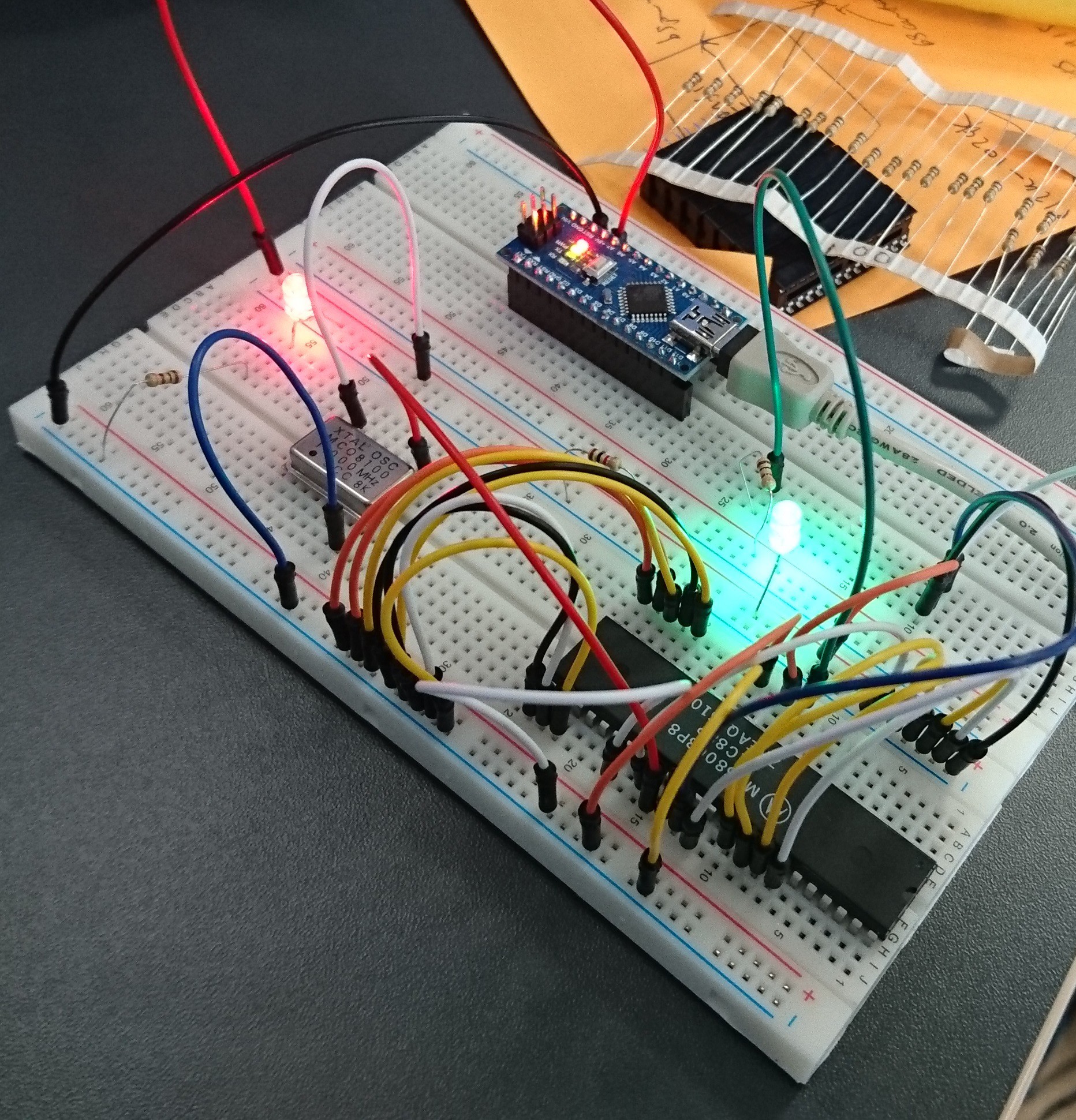
And here it is wired up!
In this image the Arduino is used simply to provide 5v DC from a USB port.![]()
The green LED is our A19 signal. The red LED is showing the board is powered.How fast does the green LED flash?
The CPU clock is 1 MHz. Each cycle is 1 us. Each bus cycle is four clock cycles. Consulting the manual, a bytewise immediate OR with a data register destination takes four read cycles - that's 16 cycles for the OR. 16 us. We can therefore run 1000000/16 = 62500 instructions per second.
The address space is 1 MB in size and each instruction is four bytes. So that's 262144 instructions. We'll go round the address space in 4.2 seconds, which means the LED will turn on for 2.1 seconds then off for 2.1 and then on for 2.2 for ever more...
Change the clock speed or pick a different address bus pin for the LED and it'll flash a bit faster! The journey has begun...
 (By Konstantin Lanzet (with permission) - CPU collection Konstantin Lanzet, CC BY-SA 3.0,
 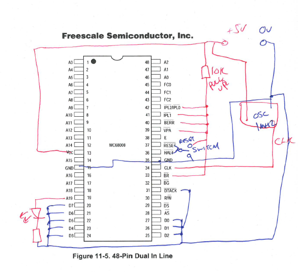 Notable connections