Close
0%
0%

The Jolly Tagger SAO

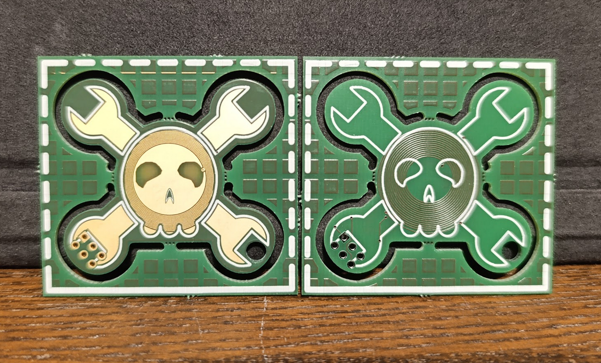
Its a NFC Tag, a Keychain pendant, a pin and a blinky Jolly Wrencher in ONE SAO !

Similar projects worth following
A important thing at a con is to meet new people and exchange contact data. And what easier way to do that is to just put your contact data/links on an NFC tag?

But just slapping a sticker tag on a cutout would be boring.

So by following the scientifically proven "i have no idea what im doing" method, i try to make this SAO using a NFC-Tag IC and a PCB trace as a coil.

The data can either be written using an NFC-app or I2C. The eyes are lit up by an PWM input on the GPIO.

And also after the con, you can just desolder the connector and use it as a keychain pendant or button pin and keep the NFC function ; )

Also: shiny golden ENIG 😍


This design however is far from perfect (at least in my POV) but i learned a lot and thats always good.
So this might be the final version for the contest, but i really want to move on to fix a few mistakes (see my last LOG entry)

The deadline is coming to an end and its time to hand in my creation and start documentation.

Functionally it works as any other NFC tag and can be written/read with the app of your preference. See my project LOG.
Alternatively its also possible to be controlled via I2C, however since the deadline is so close i cant really learn the inner workings and write a good manual. Please forgive me 😞

But lets begin with the circuit itself.

The used parts with Digikey links can be found below. The Circuit itself is very straight forward. The connector is a direct takeover from Twinkle Twinkie´s library.

Resistors "Bx" are 0Ohm bridges to keep the PCB a 2 layer one and not making any traces visible on top.

U2 is the coil, designed as you can read in my project log.

C1 is an "i am scared" optional capacitor (or inductor) just in case i would need something to tune the antenna. Jumper JP2 is to bypass that (so it needs to be closed in this version). -> C1 and JP2 can be removed

JP1, 3 and 4 are more interesting. They are meant for experimentation with the energy harvesting function of the IC. (of course after the SAO connector as been removed).

All other components are pretty much self explanatory.
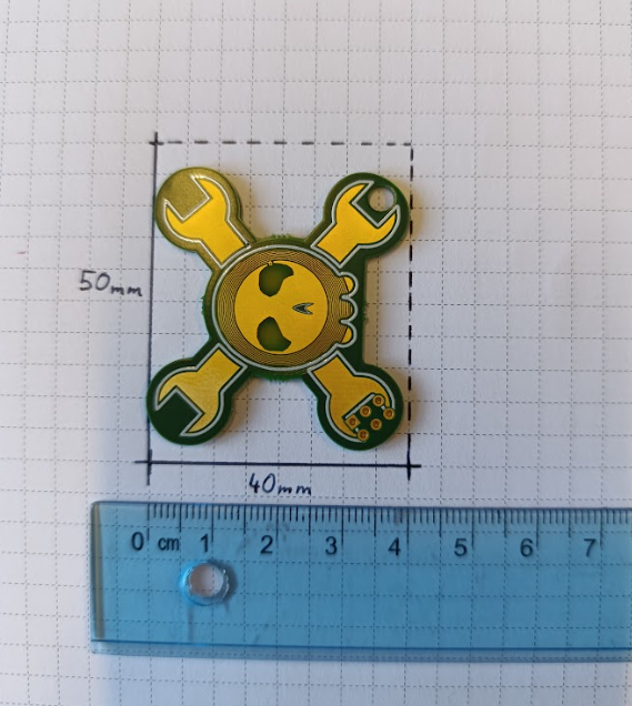
The size of the SAO is also within the given specs of the contest. However, there is no definition on the placement of the connector, nor the orientation.....

On the backside you find two large spots. They are meant for the "after con function". They have roughly the size of pins.

So when you remove the SAO-connector you can either use it as a keychain (hole bottom left) or glue/solder on a pin for example.

KiCad_Project.zip

Everything you might need

x-zip-compressed - 109.31 kB - 10/07/2024 at 15:58

Download

View all 7 components

  • Final thougts

    Phil Weasel10/07/2024 at 15:42 0 comments

    Since the contest comes to an end and i wont have any time left for experimentation. I would conclude on what i learned and what i would improve for a "Version 3". The change to smaller SMD components, staying on one layer and mostly, making it GOLD were some huge improvements already. But there s still some way to go:

    First, the circuit:
    I didnt have a lot of time to experiment with the energy harvesting function. So no lighting up when reading. however, when you place your phone in front of it you wont see it anyways so its quite a useless feature.
    It would be much better to just connect the 2nd GPIO to the other eye so you can control both eyes individually (*sans theme intensifies*)

    The Art:
    As already seen in an earlier log, the solder mask and silk screen didnt work as wanted. That would be an easy fix.
    Also i would try to find some solution to maybe block more light between the traces of the coil.

    The Print:
    Ok that one is self explanatory: BLACK SILK SCREEN IS A MUST!
    But since i wanted to produce the prototypes in europe i went with Aisler. And they only do black aver a certain number of pieces.
    Also since doing this is quite expensive over time (the golden revision already broke thebudget i planned for this) and its not a sponsored project .... oh well ... 

    The "after con feature":
    I would personally remove the keychain hole and make the pin-spots diagonally for more stability. I have the feeling the use as a pin would be far more likely. (Also AESTETHICS)

    Also the "standard SAO-conector" as THT is terrible on this one. Residue makes the shiny ENIG dirty and one small mistake and you solder on the plane. This also makes removing the Connector a hassle and it looks weird.

    I would totally change that to a compatible SMD solution. Aestethically and production wise the much better route to go

  • Light test

    Phil Weasel10/07/2024 at 14:54 0 comments

    So i soldered together the prototype and the ENIG revision, its time to test the light.

    First the prototype.

    The hoped "backlight effect" is there, but the way the LED´s shine through the PCB looks vey unsatisfying. Maybe if i would have blocked the light a bit more with a full groundplane.... 🤔

    Anyways, another lesson learned. On to the star of this show.

    And woah, the LED´s are much stronger than i anticipated. We can also already see another mistake i did: the copper of the coil is surrounded by an silkscreen-free area. Thus the light also shined through between the trace.

    But on the bright side (*badum tss*) we also got a pretty cool backlight effect.

    Putting the PWM input way down <10% seems optimal and i´m quite happy with the outcome. Also we only draw around ~10mA, thats a plus.

  • Its alive!

    Phil Weasel10/05/2024 at 16:53 0 comments

    So after testing the first version i just soldered the bare minimum to the ENIG version and .....


    It actually works!

    Double checking the inductance we are around 4.7 - 4.8µH on both versions but appearently still close enough. Also my fear that the "faceplate" will block too much turned out positive.

    LED´s will be tested next week.

  • uuh~ shiny .... and a (stupid) lesson learned

    Phil Weasel10/04/2024 at 20:33 2 comments

    So after not being home for a few days i got both orders at the same time.
    The ENIG finish looks so good. It even got a pretty cool effect with its own shadow. You have to see it.
    Also i tested the non ENIG with pressing the IC on the PCB and tried the NFC with my phone .... it suprisingly worked. Gonna solder everything together the next days.

    But one important lesson learned:
    On the ENIG one, the eyes have no silk screen and the edges look pretty ugly. Thats because my plan was to "hide" my lazy sloppy copper field with the silkscreen.

    And guess what?
    You cant put silk screen on copper.
    What you say? "But Phil thats pretty much logical that this wont work."
    Where i only answer:
    Yes, i know im stupid, shut up.

    In german you say i had to pay the "Lehrgeld". Which is a nice word for "the money you waste because you did stupid mistakes and learned the hard way".

  • Some design changes

    Phil Weasel09/19/2024 at 08:54 0 comments

    While waiting for the prototypes, i noticed someting.
    Going to the about page on Hackaday, there are two versions of the logo.

    And the Hackaday.io one is golden.
    You know what else is golden?

    ENIG !

    So i did some changes to the design and circuit. Most notable:

    I played around with the coloring and made a full ENIG fill.
    Getting this on a black PCB will probably look amazing.

    Other changes are:
    - Backlight changed to reverse mounted LED´s in the eyes
    - Changed 0805 Resistors to 0603
    - Added some solder on jumpers to add functionality when the header is removed
    - Bigger coil to get the space inside the eyes
    - Added a solder spot on the back for the possibility to use as a pin ; )

    Will it work with a copper plane inside the antenna?
    I have no idea.
    But thats the fun part  :D

  • NFC Antenna design

    Phil Weasel09/16/2024 at 11:24 0 comments

    So we chose an IC to use -> M24LR04E

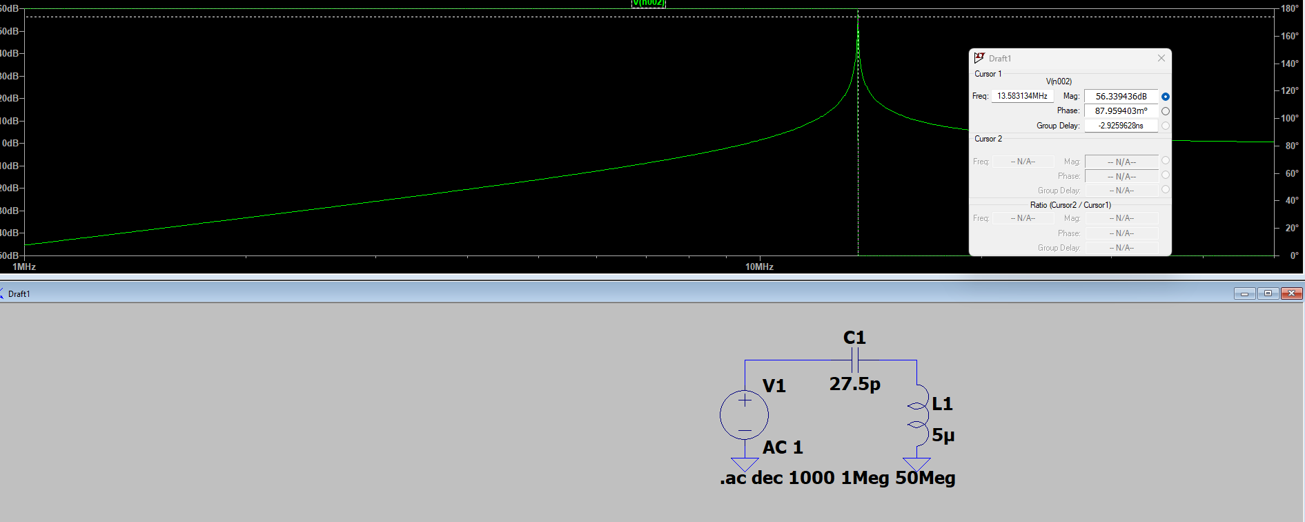
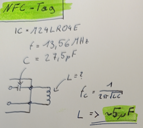
    We already know the antenna is supposed to be some sort of LC-resonant circuit. Checking the datasheet on the first page we see there is an internal tuning capacitance of ~27,5pF. The Frequency NFC works at is ~13,56MHz.

    Easy calculation:

    Lets check what LTSpice has to say:

    Seems about right.

    Next step is to get the antenna dimensions.
    I already designed the PCB outline which gives me a maximum diameter.
    Also the prototype will be manufactured by Aisler.

    So we check the Aisler design rules for the maximum dimensions.

    Input everything into a practical PCB coil calculator.
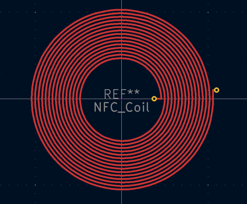
    And let the Kicad-Coil addon draw something for us.
    Put everything into a footprint.

    And voilá:

    Double checking the dimensions seem right.

    Lets cross our fingers it will work.

View all 6 project logs

Enjoy this project?

Share

Discussions

Elliot Williams wrote 09/17/2024 at 19:17 point

I love the off-to-the-side angle!  That's going to work better with the badge than you know...

  Are you sure? yes | no

Phil Weasel wrote 09/19/2024 at 09:04 point

Thanks, thats nice to hear : )

  Are you sure? yes | no

Tom Nardi wrote 09/15/2024 at 04:15 point

Great way to use I2C, and very unique idea. Love it!

  Are you sure? yes | no

Phil Weasel wrote 09/16/2024 at 07:17 point

Thanks man, lets see if it turns out as easy to use as i hope : )

  Are you sure? yes | no

Similar Projects

Does this project spark your interest?

Become a member to follow this project and never miss any updates