Why Version 2?
Version 2 of the CCD-pos project is dedicated to an upgrade of the electronics and the software to improve the signal quality, hopefully with a better measurement resolution as result. The choice to galvanically isolate the frontend electronics to reduce noise on the signal, which resulted in a complete redesign of the electronics.
Version 1 was build on a number of built-in features of the MCU, minimizing the need for additional components. The STM32L476 has two opamps and two DAC's on board, which allowed me to invert and scale the CCD-signal to bring it in range of the ADC. This setup made use of the supply voltage of the MCU, being the +5V of the USB connection with the desktop PC that analyses the CCD-signals. As the power lines of a PC may carry unwanted noise and disturbances, I decided to separate the sensitive part of my setup from these sources of misery.
What are the consequences?
The three pulse signals for the readout of the linear CCD are generated by the MCU, so they just have to pass the galvanic isolation, for which there are dedicated IC's. But the output of the CCD is an analog signal, which is not easily transferred over an isolation barrier. The choice was either an analogue isolator (expensive, possible signal distorsion) or apply a separate ADC with a handsome digital interface on the isolated side. This approach modifies the transfer of the CCD-output to a regular digital isolation. The trade-off for an amateur like me was simple: a separate ADC with SPI interface which digital signals are transferred over the barrier. There are multichannel digital isolation chips for sale, even with the specs I needed: five signals from the MCU to the isolated side and one (the SPI MISO signal) in the opposite direction.
This was the global plan, which even looks to be feasible.... However, the hash reality learned me otherwise.
The selection of the key components for an affordable price appeared to be challenging. I have spent quite some time on searching the internet for companies that sell the chips I selected to private persons for a reasonable price. Plus preferably all IC's from one source to reduce the transport costs.
AliExpress considerations.
In a situation where the budget for a project is tight, a provider like AliExpress is seductive, certainly when the experiences until now are quite positive. The downside of AliExpress is its poor searching mechanism, at least to my opinion. I find it hard to trace and compare sellers of a potential product, with additional the "strange" algorithm for the transport costs. Sometimes the transport fee is hardly depending on the quantity one buys (understandable when the total weight hardly changes), but be not surprised when doubling the quantity makes the transport explode to 5x the fee for one piece. Also the cost ratio of product vs. transport may differ astonishing between the various sellers: one must always look at the sum of product + transport to determine if a seller really has an attractive price.
The first setup with galvanic separation.
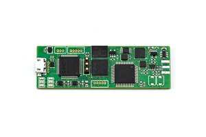
From the previous, it may be clear I bought a number of new components from AliExpress sellers, from which only one product (a number of ADC's) appeared to be flawed. Unfortunately, because my specifications went into the "high-end" products, I could not buy all IC's I selected from China, so was forced to order those from European suppliers. In version 2.0 the WeAct-F401 board is still applied, with the version 1 Marker mechanism as option, see below:
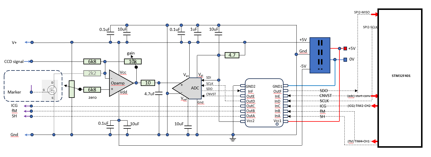
After this design was realized on a piece of experiment board, it took me a long time and quite some modifications to get it working more or less like I wanted. The unregulated DC-DC converter appeared to produce an unacceptable pollution on the supply voltage, so I had to add voltage regulators to correct that. The three timing signals for the CCD readout were generated, but didn't arrive at the connector to the cable to the CCD (see project...
Read more »
 Aleksa
 P
P
 Mark Omo