-
PCB fabricated
03/15/2014 at 22:50 • 0 commentsSo the PCB fabrication worked out nicely. I recently switched from using the toner transfer method of home fabricating PCB's to the UV exposure method because I wanted to make compact boards with small SMD components. My experience with toner transfer indicated that while this may be possible to achieve using that technique, it will be pretty hard to get reliable and decent results. So as a side-project I constructed a small UV exposure box using UV LED's I found on the cheap on aliexpress.
Using the double-sided photosensitive PCB's and developer I get from my local electronics supply store (Brigatti), making a PCB is really very easy. I am amazed at how tolerant modern photoresists are against over-exposure. After some experimentation I settled on an exposure time on my 84 LED UV box of 3 minutes, but anything from 2.5 to 8 minutes (the longest I tried) works just fine. Similarly, once exposed and developed, the remaining etch resist is very hardy. I can safely let the board sit in the etchant until all superfluous copper has been removed without loosing even the thinnest traces.
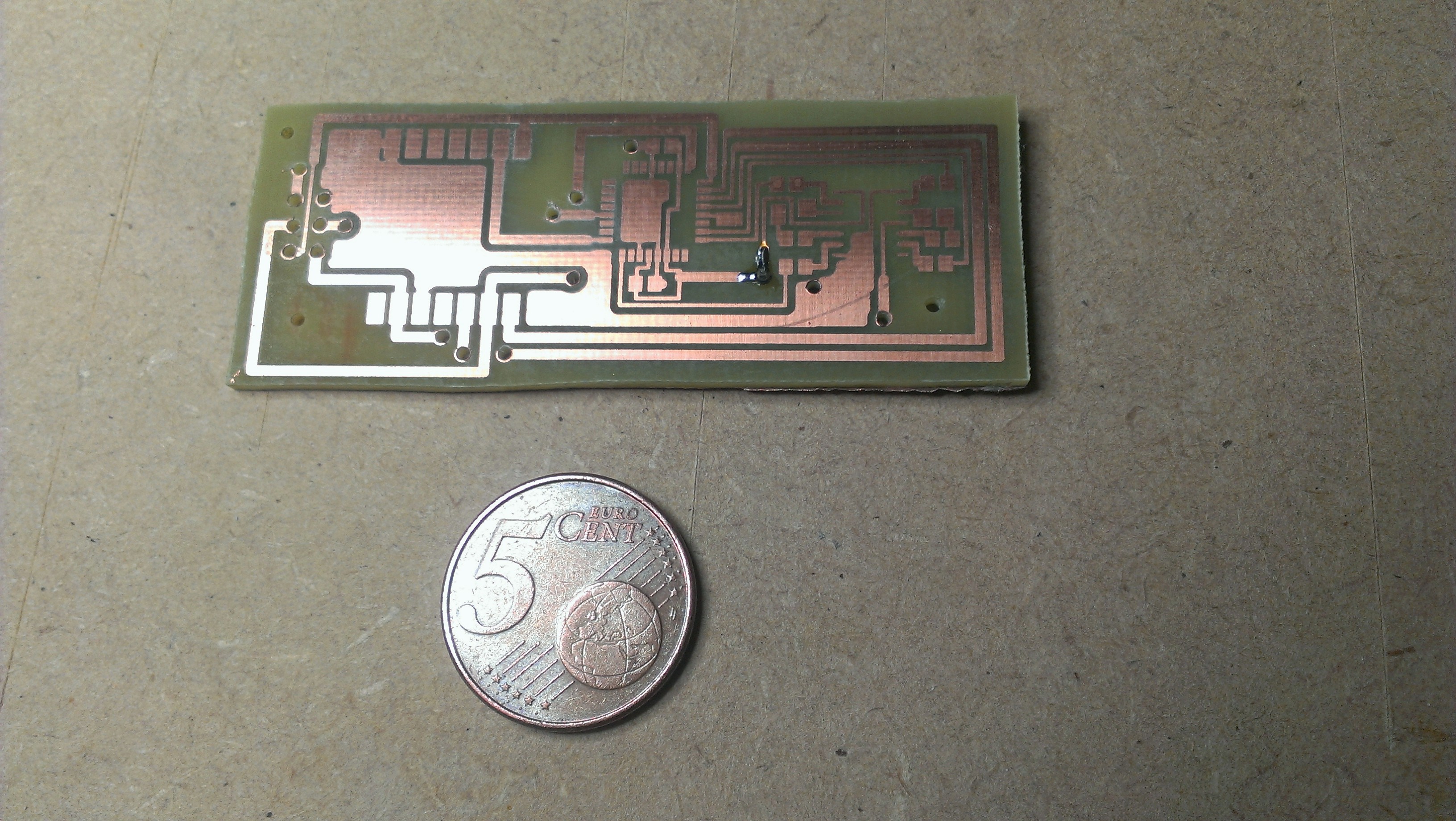
The end-result looks like this, with a 5-cent coin added for scale reference (and with one via already in place, as I forgot to take a picture at first):
![]()
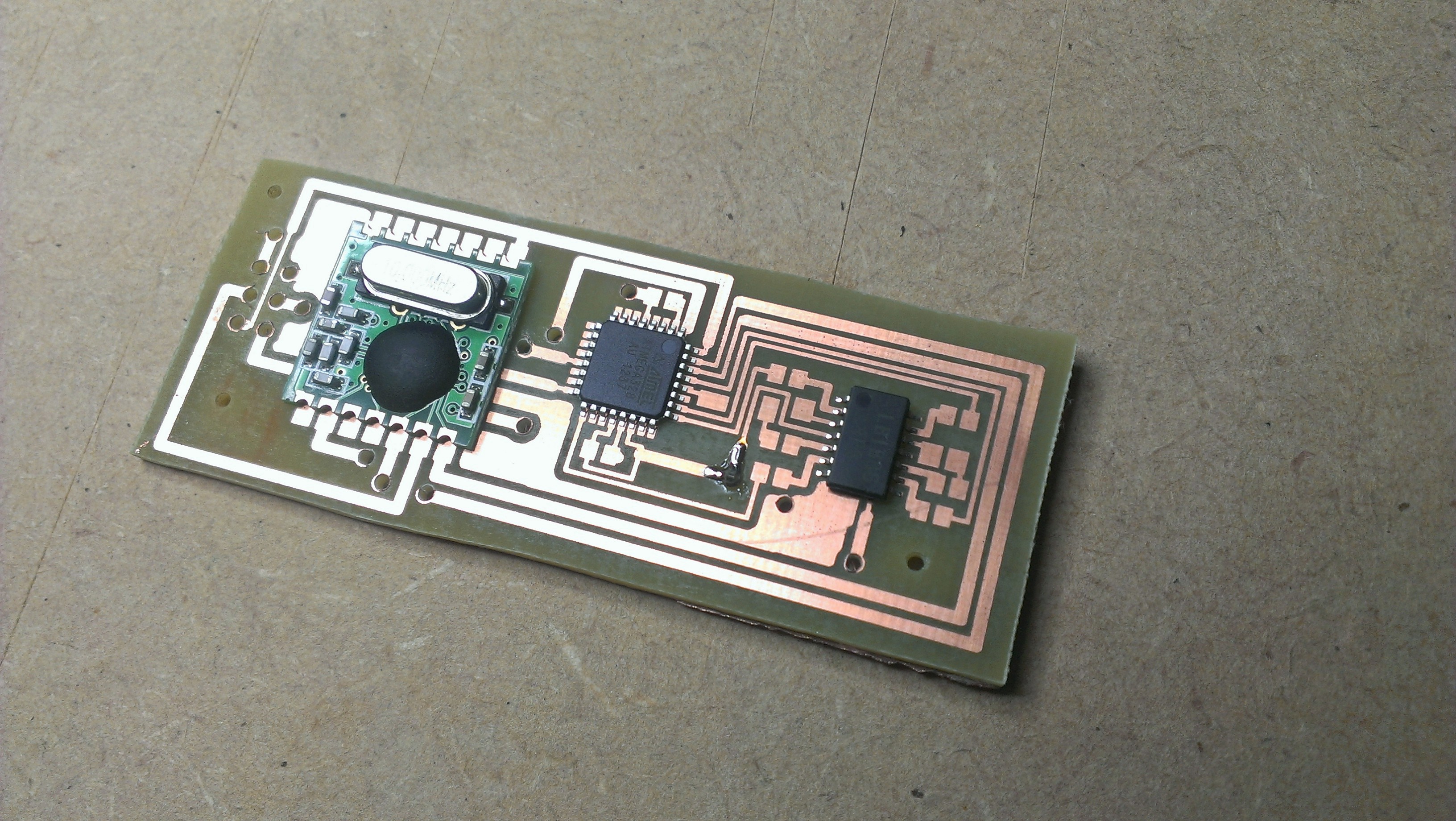
And here is the same PCB with the main components (wireless module, microcontroller and motor driver IC) laid out. The middle chip is the Atmega328P TQFP package (32 pins)
![]()
-
Ready to fabricate
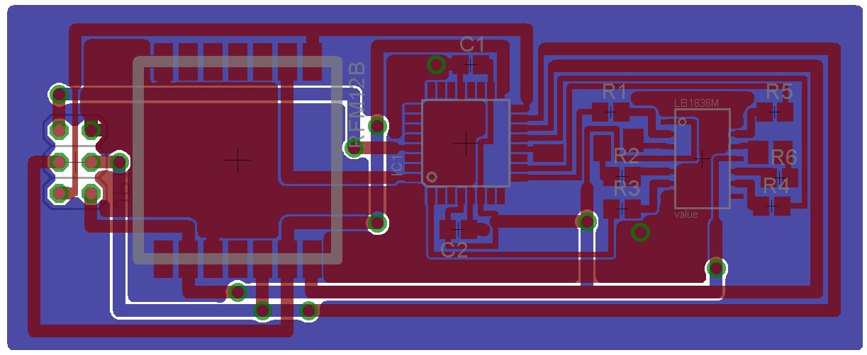
02/26/2014 at 21:09 • 0 commentsThe current state of the project is that I have a working breadboard implementation of the circuit, and all the firmware seems to be working as well. The last week or so I entered the schematic into EagleCAD and designed a PCB based on that. So I am now ready to start fabricating the PCB. I can say with confidence this is the most challending PCB I attempted to create at home yet. When working in the cad software it looks fine, but when I printed the layout (on paper, just to check) I realized it is TINY! Apart from the ISP programmer pinhead, all components are SMD's. The entire PCB is about the size of a stick of gum. I'm glad I made a UV exposure box a while ago. This would have been quite impossible to fabricate with the toner transfer method I used previously. It's a 2-layer PCB as well, although I deliberately made the bottom layer such that it can be easily done using a few wires instead. Here is the final result:
![]()
Hopefully I can show the final product in the next update.
Bruce the Shark
Airswimmer converted to be controlled using a mobile app through WiFi
 Jeroen

