 Oliver Scholz
-
1Getting started
Before you begin, a few words of caution. Building this is beyond the scope of the average DIYer. Yes, this is a project based on vintage 80s hardware, but some components are surface mount, and you must have experience soldering those! That means using a good, temperature controlled soldering iron, different tips for different solder joint sizes, and possibly spoon cartridges like e.g. the C245931 and flux as well as flux remover for SOIC. Oh, and I prefer leaded solder but suit your taste. I recommend JBC or of you’re on a budget the JaBe Chinese knockoffs. Tweezers and good magnifying glasses are definitely required.
![]()
You don’t need any special tools or programmers. You do need an EPROM programmer to burn your BIOS or games. And I have simplified the schematics by replacing a lot of gates with two GALs. Yes, old technology, but still available, and tooling is free, as opposed to FPGAs. I could have gone the FPGA route, but then you quickly end up doing everything in the FPGA, and that isn’t very retro anymore. And GALs are more manageable for the hobbyist, if you want to tinker. I recommend the TL866 II programmer, which is also able to burn GALs.
You should have a DVM. A good scope is not required, but can be very helpful to verify everything is working as it should. Even a vintage 20 MHz CRT scope will do. A frequency counter helps too, although these days a scope will do that too.
Finally: get all parts up front. If you’re into electronics, you should have most resistors (0805 unless otherwise noted) and caps (again 0805 unless otherwise noted) in your drawers, but some parts are hard to come by these days, and it’d be a shame if the project ended up 95% complete because something wasn’t available.
Most parts are available from Mouser or Digikey, RS and o5her local standard parts sources. Go through the instructions, gather which parts of the project you want to build and then compile your shopping lists.
And it helps if you team up with one or more friends, maybe building one for each? You’ll save on shipping and can fix mistakes together. -
2Power to the people
The CV doesn’t work without power, so we‘re starting with the power supply.
![]()
You can reuse a Coleco power switch made by Canal, Taiwan, even if it’s broken, as long as either side has a little life left in it. Otherwise, use a MFP201 switch, which can be used with a CV enclosure provided you 3D print a plastic extender (see “ColecoPowerSwitchCap” in the files section). You can install a LED, either through hole or SMD (1206). R64 should be chosen accordingly, typically 330 Ohms. You can also use a power jack on the PCB, or use red and black wires to extend to where the Coleco power connector is. See files section for a printed plate with a hole for the jack (“PowerSwitchPlate”).
J2 DC10LP/FCR681465P DC jack
L7 4,7uH/2A
D22 MBRS240
C6' 100nSW2 Coleco Console power switch made by Canal, Taiwan. No longer available, AFAIK.
or
SW4 MFP201N available through e.g. RS Components![]()
optionally:
R64 330 (for standard 20mA LED, adjust if necessary)
LED1 LED 5mm
or
LED1A CHIPLED1206 (right next to LED1)![]()
The remaining components are at the upper left corner of the PCB:
U21 LM2576T-5 L1 150uH L-PISR L2 22uH L-PISM D23 MBRS340 R63 47k C82 VF100/16PD C84 1000uF/16V FT-V 1M 16 C85 100n C87 HD-V 100U 25
If everything looks ok, hook up 12V supply and measure regulator input nom. 12V at TP10.Then measure 5V at TP19.
![]()
Finally, the controller section requires a -5V supply for strong pulldowns, so add:
U24 ICL7660CSA C50 10uF/10V C51 10uF/10V C52 10uF/10V Now measure -5V at TP3.
-
3Rock around the clock
![]()
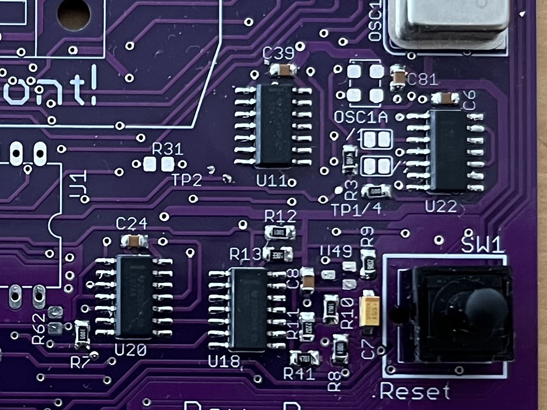
Next we're going to generate a clock or two. Or more. The CPU needs a main clock of 3.57 MHz, but those are hard to come by, so the PCB features a two stage divder. This allows the use of 7.15 or 14.31 MHz crystal oscillators in DIL8 can or XO53 SMT packages. I usually use the 14.31818 MHz crystal oscillator and divide it by 8 by default.You need these parts:
OSC1 14,31818MHz (e.g. Mouser 815-ACH-14.31818EK) U22 74LS74D C81 100n C6 100n R3 47 Ohms /4 0 Ohms (or use /2 or /1 solder jumper for different crystal freqencies) optionally: solder pin or loop to "GND" above OSC1 for measurements.
Measure 3.58 MHz 5V square wave at TP1 and U1 Pin 6
![]()
-
4Video processor clock
This step is optional! If you are using Pico9918 or F18A, you can skip this step. If you’re using a separate crystal for the VDP, you can skip this step! However, if you want to use the existing 3.57MHz clock and triple it, follow this step.
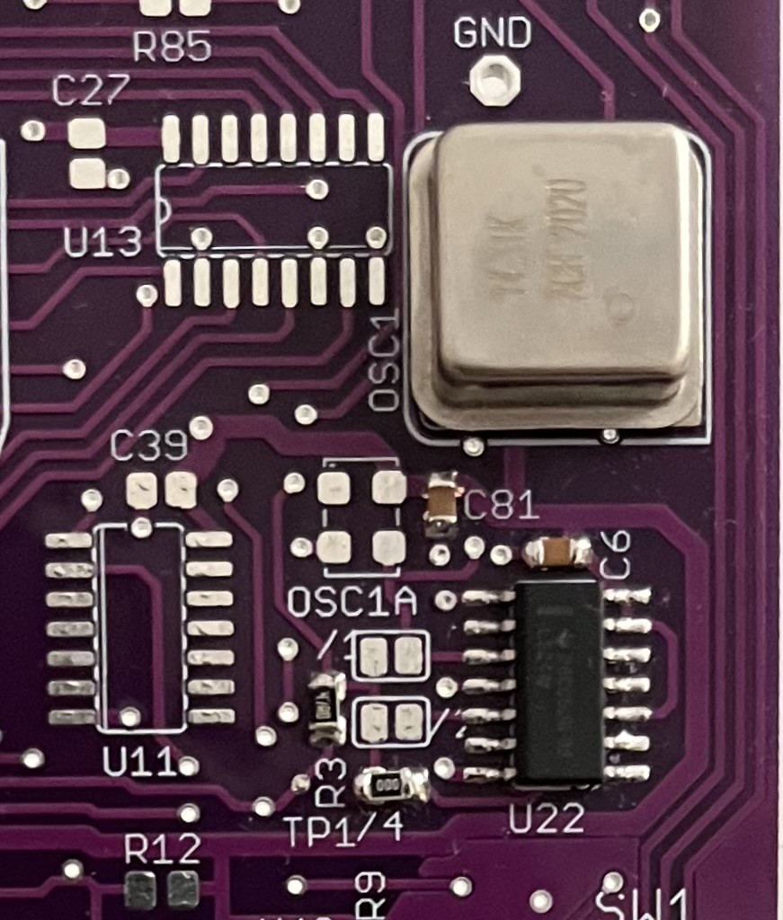
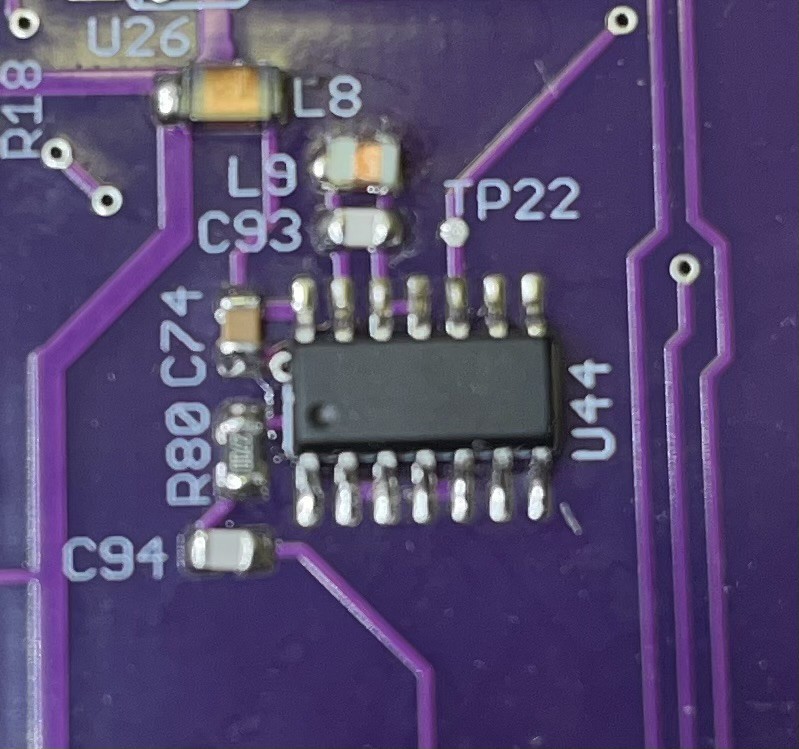
![]()
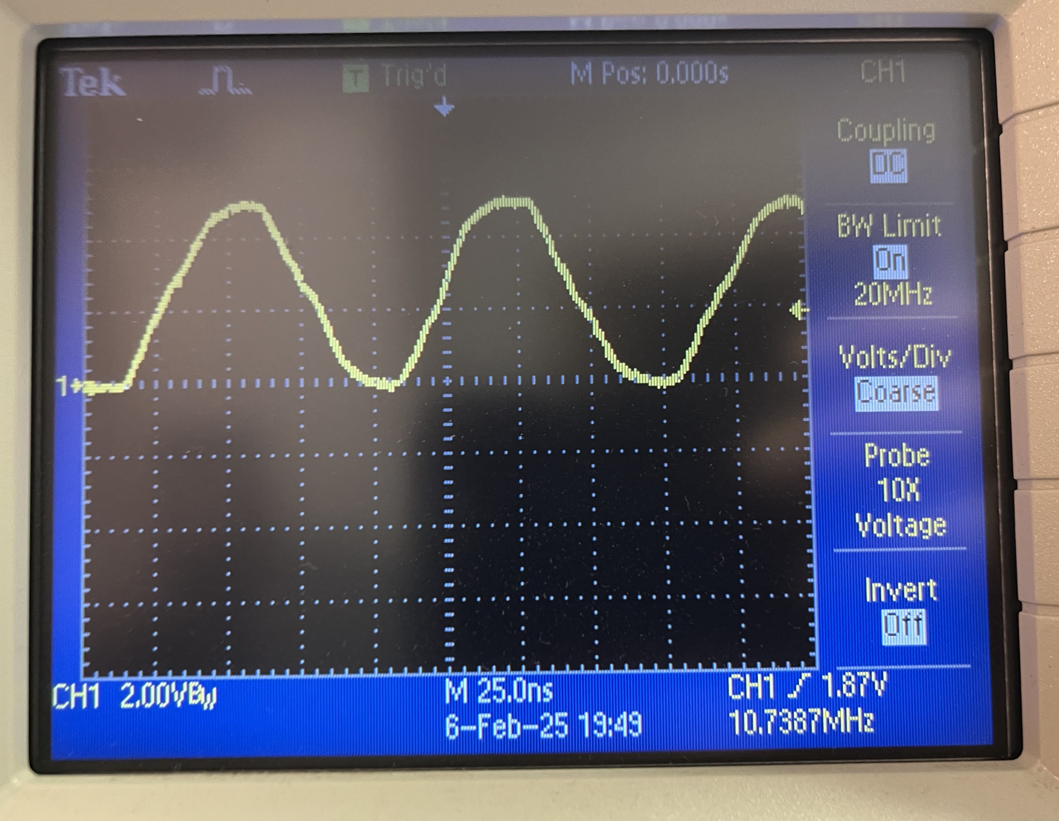
U44 74HC14D L8 10uH 1206 L9 2,7uH 0805 C74 100n C93 82p C94 100p R80 270 Verify 10.737 MHz at TP22
![]()
-
5Basic reset circuit
Next up is the reset circuitry. Very few components, see image. The board can host the original CV switch, or the Bourns alternative. If you use the Bourns alternative, 3D-print the little “ColecoResetWasher” and slide it over the stem. Now the Coleco actuator will work with the new switch.
Important: until you install the reset/pause controller U14, short (install solder jumper) U14 Pin 1 to Pin 2!
![]()
U18 74LS05D SW1 BOURNS 1543-650-149 C7 1u/6.3V (3216) "A" C8 100n R8 1M R9 91k R10 1k R11 22k R12 1k R13 3k3 Verify U1 Pin 26 high, going low when reset switch is pressed
-
6Sound clock and wait signal
Now add two more ICs, these are responsible for the sound clock and wait state circuitry compatible with the original CV.
![]()
The parts are right next to the previous steps‘ clock and reset circuits.
U11 74LS04D U20 74LS74D C24 100n C39 100n R41 4,7k R7 1k
Verify U1 pin 24 is high. Also measure 1.79 MHz 5V square wave at TP2![]()
-
7CPU & Expansion port
Now it's getting serious. Just a couple of pullup-resistors and a socket, but a few things to verify. Most parts are right around the CPU.
U1 Z80A CPU R4 3k3 R5 3k3 R6 3k3 R31 3k3 R60 470 Ohms R61 1k R62 1k R65 3k3 C4 100n C78 100n C89 22uF/16V Tantalum bead ![]()
Verify socket U1:
- 5V between pins 11 and 29
- Pin 6: 3.57MHz clock
- Pin 26: Reset
- Pins 16, 17, 18, 24, 25: high
-
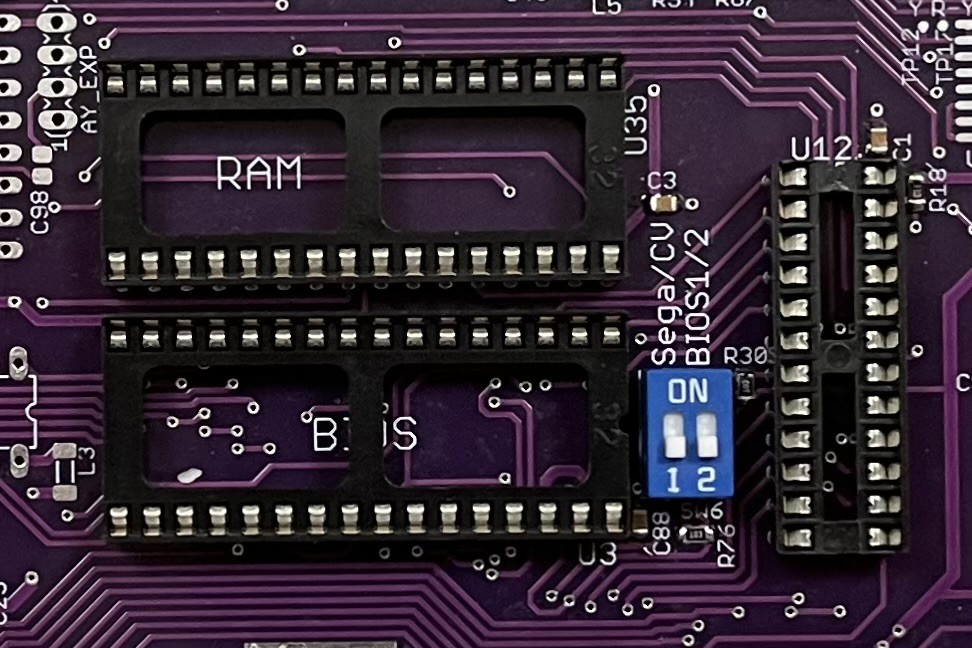
8RAM and ROM
At the very least a CPU needs some ROM, at address 0000. so let’s solder sockets for BIOS and RAM. And to map ROM correctly, the address GAL is required too. And while we‘re at it, also install the two DIP switches and pull-ups.
![]()
U3 27C010 EPROM U35 TC554001AFP32 U12 ATF22V10CXZ R18 3k3 R30 10k R76 10k C1 100n C3 100n C88 100n SW6 DIP-Switch 2x Leave RAM socket open, insert Address-GAL in socket U12, install the CPU and program binary "CPUTEST.IMG" into a 27C010 EPROM and install it. The test EPROM is just a short program that can be monitored on a scope, it only uses the bottom few bytes of BIOS in an endless loop.
DIY ColecoVision
My goal was to create an enhanced drop-in replacement for the ColecoVision that you can build at home using available components.


Discussions
Become a Hackaday.io Member
Create an account to leave a comment. Already have an account? Log In.