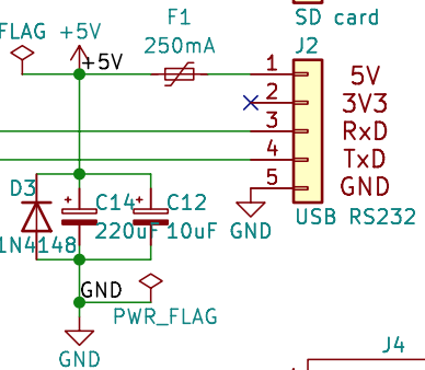
Power supply
The power for this board is provided by the USB-to-Serial converter. A 250 mA polyfuse protects against damage in the event of a short circuit. A red LED indicator lights up when power is available.
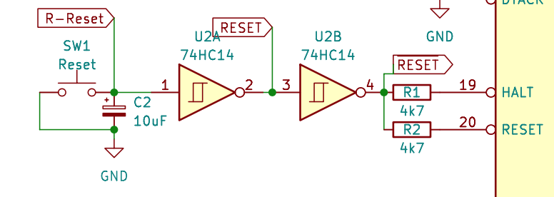
Reset circuit
The reset signals are generated simply by a 10µF capacitor, which is charged through a 10k resistor. Two Schmitt trigger inverters (74HC14) are used to generate the positive and negative RESET-signals. Since both the 68000's /RESET and /HALT-signals are bidirectional (input and output), they are connected through a 4.7kΩ resistor.
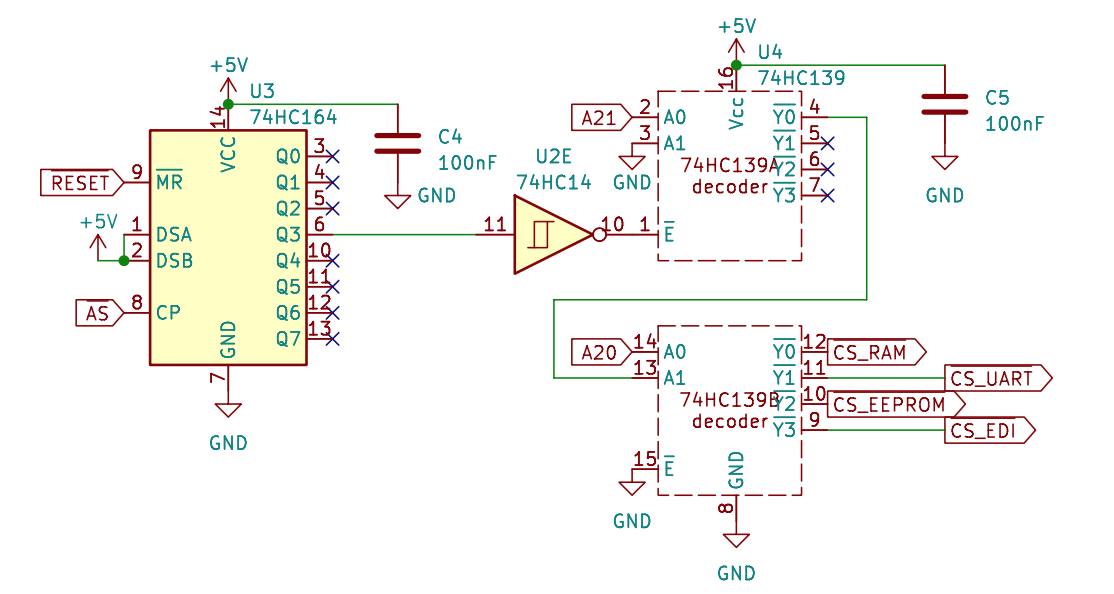
Address decoding
In fact, the address decoding is arguably the most fascinating aspect of the design!
In the simplest 68000 designs, the EEPROM is fixed at address 0x0000. After a reset, the CPU expects the stack pointer and start address to be located at 0x0000 and 0x0004, respectively. All interrupt vectors are in the next 1kB till 0x03FF. If these vectors are fixed in EEPROM, it limits flexibility, especially when attempting to run the FUZIX OS.
A solution is to switch out the EEPROM and switch in the RAM after the first four read cycles. This is the exact purpose of the 74HC164. After a /RESET, all Q-outputs are initially low. The /AS signal is used as clock, and after four (16-bit) read cycles, the Q3 output goes high.
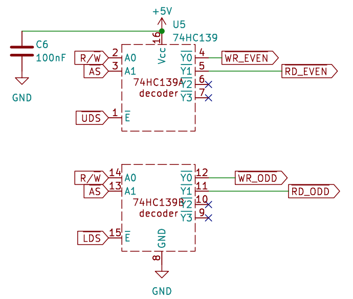
The 74HC139(a) is connected as an OR-gate (I used this complicated way because I didn't want to add an extra OR-chip and I had one decoder left.) The first four cycles the /E input is high, so all the /Y-outputs are high. The /Y0-ouput is connected to the A1-input of the second (b) address decoder, and thereby switching in the EEPROM in the first four read cycles.
After the four read cycles, the /E signal is low, and /Y0 begins to follow A21. From that point onward, the RAM is mapped to address 0x0000.
CF-card interface
For CF-card, we need different timings. First the /CS have to be activated, and then the /RD (of /WR). The /RD needs to de be activated before /CS becomes inactive. For EEPROM and RAM these timings are irrelevant, and may be simultaneous.
In the 68k-nano design (by Matt Sarnoff), I found a solution. In typical 68000 address decoding, the /AS-signal from the CPU is connected to the /E-input of the 74HC139 decoder. However, you can bypass the /AS-signal by grounding the /E-input. This causes the /Y0 to /Y3-outputs to become active earlier (before the /RD and /WR-signals). The downside is that one output signal is always active, even when there is no bus activity. I built the 68k-nano, and this works perfectly fine.
So pin 15 (/E-input) is grounded for the correct CF-card timing.
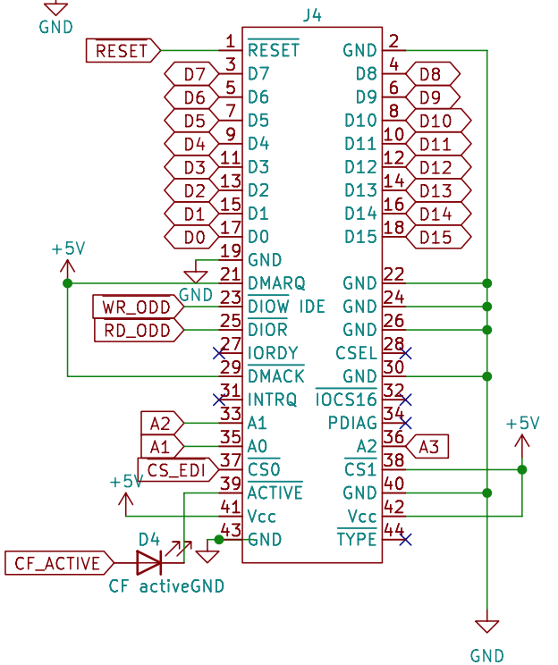
Warning: THE CF-CARD IS UNTESTED YET!
R/W-signals
The 68000 has a 16-bit bus, and the upper (odd) and lower (even) bytes can be read or written individually. Therfore four signals are required: /WR_even, /WR_odd, RD_even and /RD_odd. These can be generated using a 74HC32 (4 OR gates) and an inverter. However, a single 74HC139 can also generate these signals.
As you can see, the /AS signal is also used as enable input. This means that the /RD and /WR signals only become active when the /AS (address strobe) is active. In this way, the absence of /AS in the address decoding is compensated.
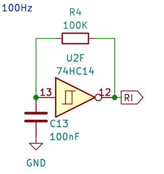
100Hz oscillator
For task switching and basic timing, a 100 Hz RC oscillator is added. A 100k resistor charges a 100nF capacitor, and the Schmitt trigger generates a clean square wave, which is connected to the RI input of the UART. This generates periodic interrupts.
While the RC combination is not highly precise, the capacitor can be selected to achieve the desired 100 Hz signal.
UART, IO and interrupts
The UART TL16C550 is an excellent chip. It features 2x16-byte receive and transmit buffers, four input and four output lines, and it can handle the 100 Hz interrupts for the CPU.
The SD-card interface...
Read more »
 spudfishScott
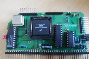
 EtchedPixels
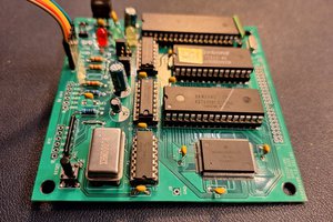
 6502Nerd
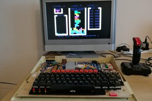
Hi Soni, the SBC only draws about 100mA, so powering by a power bank is no problem. I have no intention to add a dedicated keyboard or screen to it. The whole idea is KISS; keep it simple. I use a macbook as “terminal”. (Sometimes I use it on the kitchentable-off grid). You could use any (cheap) laptop / chromebook as a terminal, and powered by a USB232 it is “mobile” ;-)