 Sebastián Elgueta
The Current Status
At the moment, the system has no electronics inside the chamber, being purely mechanic. This was an initial design choice in order to simplify the initial design as a proof of concept. However, it's quite clear that the lack of any 'in chamber' diagnostics or feedback severely affects the whole system usability and reliability.
As the proof of concepts was partially successful, it seems appropriate to tackle the increased design complexity in order to improve the rate of development.
Goals and Constraints
Overall, the intention of the proposed modifications are:
| Goals | Solution | Challanges |
|---|---|---|
| Enhance deposition quality | A resistive substrate heater is incorporated | Heat Dissipation, high current input, requires temperature feedback, possible damage to the tape |
| Make the system more reliable and autonomous | Positional feedback on the mechanical components status | High pin count, relatively difficult mechanical placement of sensors, perhaps signal conditioning considerations |
| Film Diagnostics | In situ electrical measurements, Incorporation of a QCM sensor | Required rotational electrical 'pass through', signal multiplexing is a must, connectors are no trivial |
Due to the evident space constraints inside the chamber, the rather small amount of available flanges and the cost of electrical feedthroughs, I think it's quite clear that the way to proceed is to incorporate microcontroller(s) inside the chamber, which may reduce the pin count and allow signal transfer to the overall control system through serial interfaces.
At least in my experience with vacuum hardware, this is a highly unorthodox solution, probably due to contamination and heat dissipation concerns. For the vacuum levels I'm working, the contamination doesn't seem as big a problem as the possibility that my electronics might get fried without precious air to dissipate the heat they generate. But let's trust metal-cored PCBs (and perhaps some exotic potting compounds) may help.
The final constraint is the amount of pins available in the electrical feedthroughs. I only have a couple of KF25 flanges available in the covers, and therefore I bought a couple these feedthroughs:
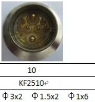
I have no idea about the current ratings, but I intend to use the thicker wires for the heater (which draws about 3A at 24V) while the 1.5 mm ones could be used to power the circuits inside.
High Level Diagram
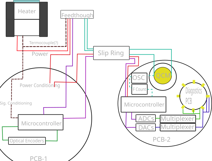
While I still haven't fully committed with all the components and design choices (should I try to implement the QCM oscillator and frequency counter inside, or rather just use an external dedicated instrument, for example), the overall system is based on at least two PCBs: One coupled to the feedthrough cover, which hold the main microcontroller, which should take care of most of the IO workload (reading rotary encoders, communicating with the main controller, sending instructions to the other PCB) and a 'smart shutter', which replaces the existing one and holds the film diagnostics tools. Future logs shall dive deeper onto each of the systems components.
Discussions
Become a Hackaday.io Member
Create an account to leave a comment. Already have an account? Log In.
Not necessarily... while substrate temperature does play a role on film adhesion, usually its less relevant than material properties and the energy of the species in the plasma cloud. Is critical for film quality, though.
I think that what you are describing seems quite hard for a 'parallel' lithographic process, where al features are defined at the same moment (as it's quite hard to maintain such thermal gradients). It could be a cool idea if performed sequentially for thermally mediated CVD, sort of a thermal printer but for functional materials ;)
Are you sure? yes | no
Thanks for the info! This is why I generally stick to computer science. :-P
Are you sure? yes | no
If I understand the concept correctly then parts of the plasma cloud will only (reliably) affix themselves to parts of that substrate that are hot enough. Have you considered hitting the substrate with the the lithographic pattern you want to make it just hot enough for the plasma to "prefer" sticking to the part of the substrate that you want it to? If you were able to inspect the results then you could make it a multicycle process.
Just a thought.
Are you sure? yes | no