 deqing
-
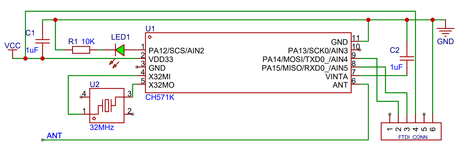
1Schematic of the circuit
![]()
-
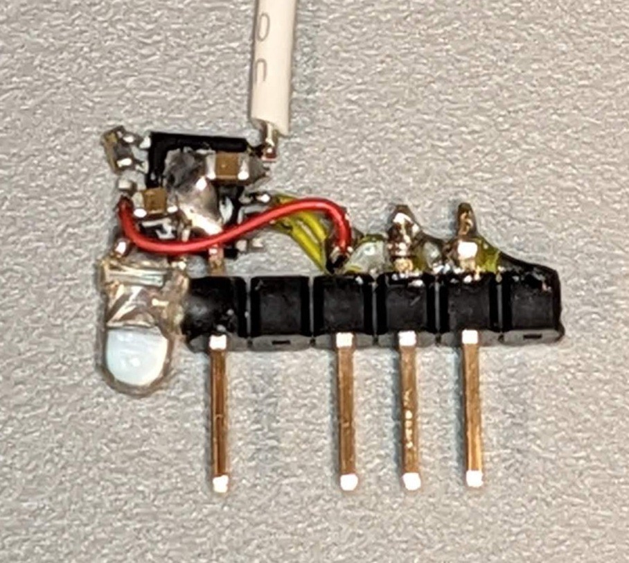
2Back photo
![]()
-
3Solder tips
- The exposed pad is connected to pin 3 GND internally. The two capacitors can be soldered directly from the exposed pad to pins 2 and 7 for decoupling.
The crystal can be soldered directly on pins 4 and 5. - The LED can be soldered between pin 1 and the exposed pad.
- The antenna can be soldered on pin 6.
- The FTDI connection GND pin can be soldered on the exposed pad for support, and the 3.3V, TX, and RX can be connected with wire.
- The exposed pad is connected to pin 3 GND internally. The two capacitors can be soldered directly from the exposed pad to pins 2 and 7 for decoupling.
-
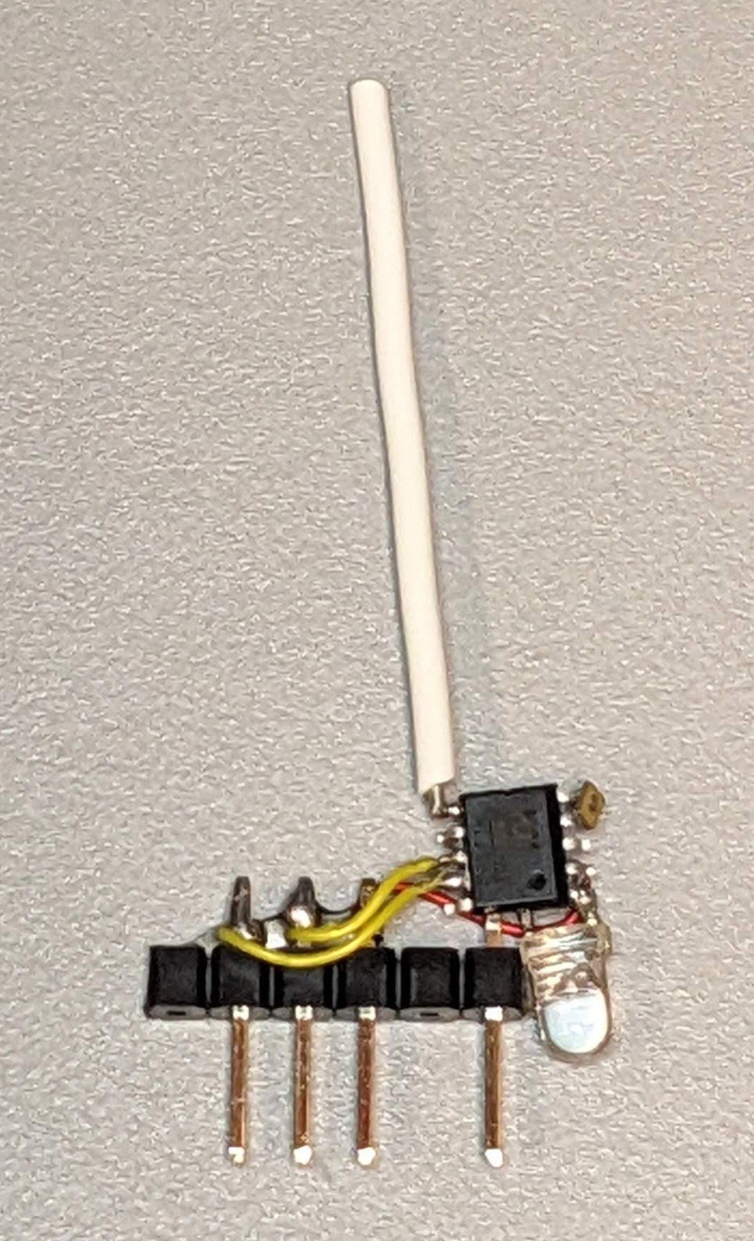
4front
![]()
-
5Add some protection
I used high viscosity UV glue to pot the whole circuit for protection.
Discussions
Become a Hackaday.io Member
Create an account to leave a comment. Already have an account? Log In.