bru3s
bru3s-
Finally some progress on rev. A
01/04/2026 at 20:58 • 0 commentsHi,
happy new year!
I'm finally managing to share some (very) long overdue progress on the state of the board, after a months-long hiatus due to work and unrelated issues.
After finishing the design of the initial revision, I ordered two board prototypes from NextPCB, who did a very good job on the resulting hardware and in supporting engineering questions, as well as handling PCBA. I was very satisfied with their service.
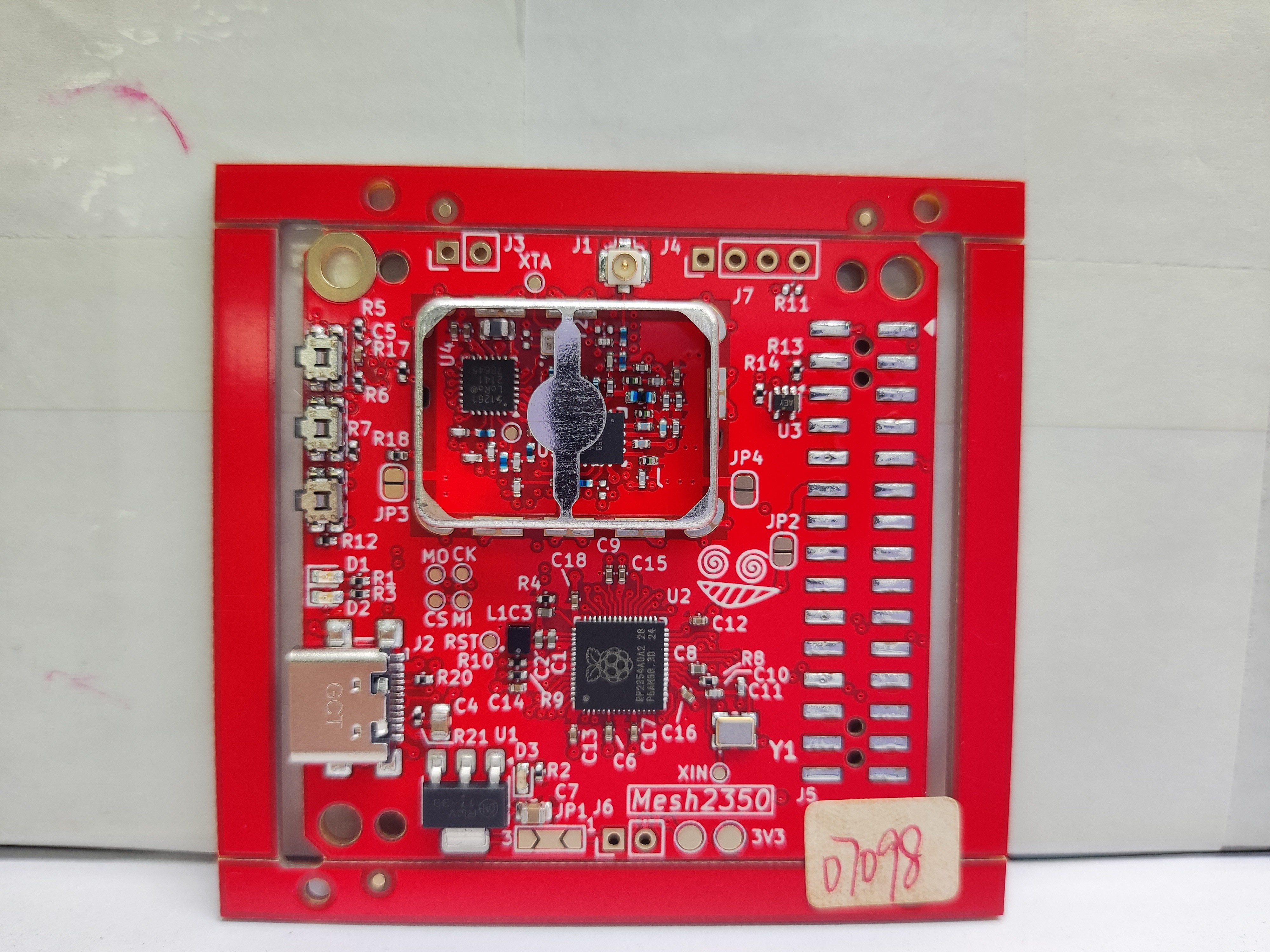
Below you can see a board with all the components on, as shared by the engineering team at NextPCB:
![]() The bringup procedure
The bringup procedureBringup is fairly straightforward, especially in standalone mode (i.e. powered by USB):
- Connect USB cable to a PC port with a proper USB-C cable
- Measure voltage on pin 3 of JP1 -> should be around 3.3V
- Disconnect USB, close 2-3 of JP1
- Reconnect USB while keeping SW2 (BOOTSEL) pressed (button in the middle)
- RP2354 should mount as expected
- Load test firmware into memory
- Check if LEDs blink and messages are sent via the USB virtual serial port
- Disconnect USB, close JP3
- Reconnect USB and, using the test firmware, check that the connection with SX1261 is working as expected
- Disconnect USB, close JP4, connect a proper antenna via J1
- Reconnect USB and, using the test firmware, check frequency synthesis and infinite preamble mode with an SDR
With these steps, all major functional blocks - except the M-BUS connection - can be tested.
So, since this is the first revision of the board, I inevitably ran into issues almost immediately when performing the procedure :)
RP2354 woes
As mentioned previously, I wanted to tinker with the RP2354 (thanks to production samples offered via NextPCB) instead of other microcontrollers in order to save board space that would have been taken by the QSPI flash. It somehow would have fit on the board if I wanted to, but again, I just thought it would have been more interesting to use the new version with internal flash.
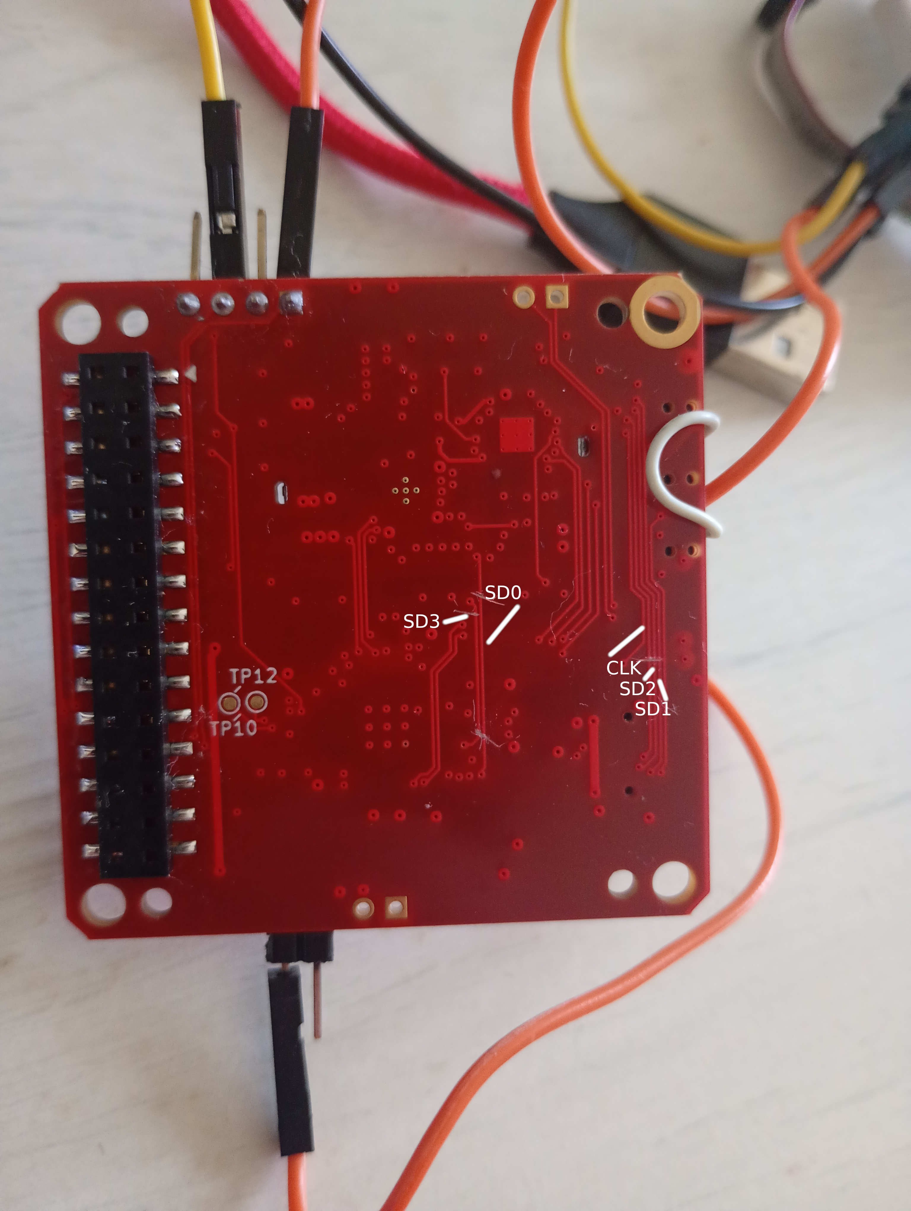
Unfortunately, when routing the board, I missed an important section of the RP235x datasheet, i.e. 14.3, which states that
"The six dedicated QSPI pads on the RP2350 die (CSn, SCK and SD0 through SD3) connect to both the internal flash die and the external package pins. [...]",
which in turn means that if you're using the version with internal flash, you should leave those pins unconnected, otherwise you're possibly directly affecting the signal levels of the QSPI bus.Having missed that, I proceeded to route the SX1261 DIO, RST and BSY signal to those QSPI pins, since they were pretty convenient due to their position and facing direction. Oops.
You can read more information about this whole "investigation" on the relevant thread on Raspberry official forums. Suffices to say, the RP2354 would show up as a mass memory, ready to accept UF2 files, but would not run the executable correctly. To mitigate this, the offending traces had to be cut away.
![]()
With this (pretty ugly) hack I was able to finally boot functioning software via the UF2 loader, confirming that at least the rest of the circuit for the MCU was working as expected.
Another issue I encountered though, was when I tried to connect a J-Link debugger to the SWD port (J4) to make sure the debug functionality was operating correctly. That also led to all matter of weird issues when trying to upload the firmware via the debugger. This was confirmed a debugger side issue by Segger support themselves, stating that the capability to interface with the RP2354 is currently planned, but still not implemented.
Despite this, if the flash step is skipped and the debugger is only used to analyze execution of the existing firmware (i.e. via UF2), everything works as expected (except maybe flash breakpoints - still haven't checked those).
Mechanical issues
The overall height of the board with its largest (tallest) elements does not quite fit beneath the M5Stack Core, at least not with the headers that M5Stack provides. I could see two possible solutions for that:
- replace the RF shield with a narrower one, since the current one is larger than it needs to be
- use a different male header with longer pins so the distance is increased properly
SX1261 crystal pads
I had a minor (but still significantly annoying) oversight when making the footprint of the crystal for the SX1261, and ordered the pins off by one. Fortunately a fix could be done just by desoldering the component and rotating it by 90° - the pads would still overlap enough for soldering it again in the correct position.
Accessibility
- The test points arrangement could be improved. I think I'll move all of them on the same side, possibly the bottom one. It would also be nice to have all of them arranged in a grid of sort, so to make a test PCB
- Power supply test points are a pain to use, it'd be better to turn them into 2.54" plated holes or castellated holes/pad for alligator clips.
- The debug header is alright, but since there's enough space for it, it'd be way more friendly to mount an ARM 10 pin connector
- Buttons are preeetty tiny. Sometimes too much when you're trying to put the board into mass memory mode.
Odds and ends
- The user LEDs light up faintly when the GPIOs are not configured yet, and I'm unsure why. I haven't investigated it yet, but maybe it is to be expected..?
- The test point on the SX1261 oscillator isn't really useful, at least for the tools I'm equipped with.. it is already fast enough that trying to probe it disturbs the operation
Moving forward
For the time being, the priority is to go on with testing the board in terms of power and sensitivity, performing e.g. range tests. Then printing a case for it would be also useful.
Eventually the board will undergo a revision as described above, but it'd be probably better to try some porting of meshtastic or meshcore on it, or at least interface it to the M5Stack Core - indirectly due to the height issue - so that other shortcomings can be discovered beforehand!
-
Interface with M5Stack "Faces" and ports
05/07/2025 at 18:38 • 0 commentsAs mentioned in the project description, one of the driving forces behind the form factor of the PCB was that I had some products from M5Stack lying around unused, among which the original Core Grey and an expansion module called Faces (specifically the 2nd version), which adds some LEDs and a keyboard.
![]()
I specifically wanted to make a T-Deck-like device, so I set forth constraining the PCB dimensions and positioning of components to that.
A note on standalone mode
The project specifications included a "standalone" mode and a "module" mode; these are two ways the device can be used, depending on whether it's mounted as an M5Stack compliant device or not.
- In module mode, the RP2350 is treated as an SPI slave, receiving commands from the ESP32 core such as "set the power" and "transmit". In this mode
- The USB port is not used for power supply
- VBUS from M-Bus is used instead
- The RP2350 either interprets commands or acts as a passthrough to the SX1261
- it has no agency of its own (e.g. spontaneous transmission)
- LEDs are treated as simple device indicators
- user button events are relayed to the ESP32
- serial debug is still used (possibly even USB, but unlikely)
- In standalone mode, the RP2350 is instead used as either transceiver connected to the USB and receiving similar commands as if it was in module mode, or it reacts to time events or user button clicks to decide when to transmit. In this mode:
- The USB port is used for power supply
- VBUS from M-Bus is not used
- SPI port to ESP32 is unused and can be configured as free GPIOs
- user button events trigger actions fully within the MCU firmware
- serial debug and USB interfaces are both used for logging and communication
Ports
The ports I wanted to have with the outside world were as follows:
- USB-C for communication, programming and power supply
- separate VBUS header to measure power consumption
- M-Bus header for module mode and generic GPIO interface
- serial port for logging and debugging
- SWD port for serious debugging
Additionally, I added 2 RP-controlled LEDs to indicate status, errors and whatnot to the user; three switches for RP boot, reset and custom action; and a power LEDs to quickly check 3v3 status.
M-Bus
The M-Bus interface follows the orientation used in the Faces II module; so that the bottom of this board will have to mount the female socket, and the male one to propagate that of the faces base.
The following signals have been routed through it:
- Power
- 3V3
- GND
- RST signal to RP2350
- Independently controlled with default asserted for RP (with pulldown)
- RP reset line towards SX default asserted (with pulldown)
- Note that per Core Grey schematic, the reset line from the ESP32 is low pass filtered
- Independently controlled with default asserted for RP (with pulldown)
SPI
- default pins + additional SS
Interrupt line
- used by RP to signal TX done/RX done
BSY line
- used by RP to signal operation in progress
The RST line was a bit of a pickle since I wanted the OR'ing of all possible sources, but didn't want to do that via diodes. So I decided to put a dedicated IC, i.e. the SN74AHC1G08 (SN74AHC1G08DCKR for smaller SC70-5 footprint) with an additional line from the SWD via a simple resistor.
Also, the M-Bus has also to control the Faces device, which takes up the following pins of the ESP32:
- G15 (leds)
- G16-G17 (GROVE port A)
- G26-G36 (GROVE port B)
Ports placement
From the attached figure, you can see that there are already two limitations regarding the position of ports and headers:
- on the right side, the M-Bus (can't see that from the picture actually, but you can check M5Stack docs) takes up most of the available board outline
- on the bottom side you have the keyboard
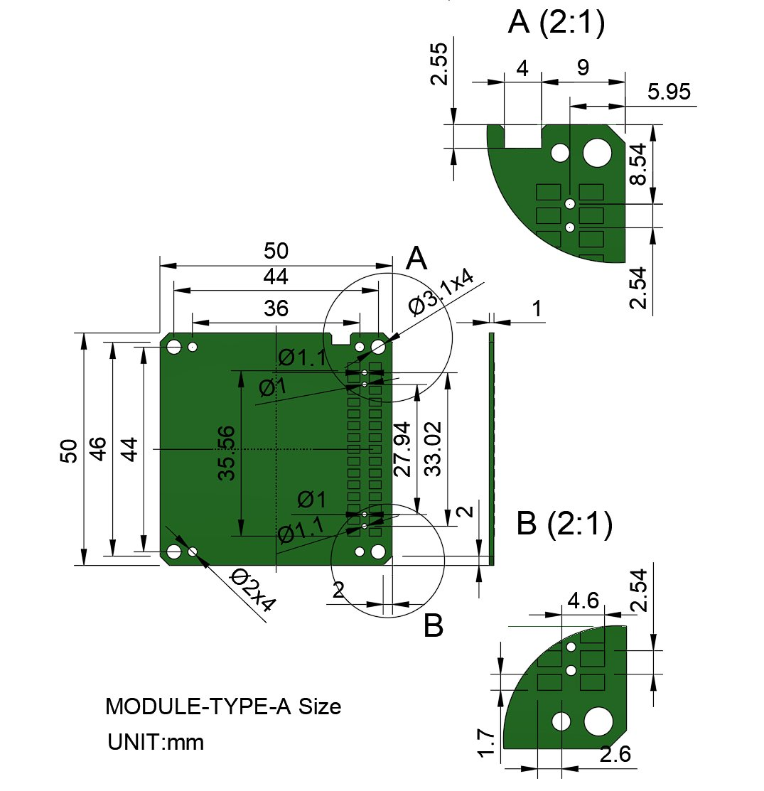
You can see the general outline of the board from the picture below.
![]()
So I ended up placing the ports I was most interested in to the left and top side of the PCB.
In particular,
- I've placed the USB port to the left to be consistent with the charging port of the M5Stack and to not have awkward pulling forces on the same side as the antenna connector;
- Buttons were also placed on the left side so you can reach them easily with your fingers (for right handed folks at least) when holding the device, and LEDs close to them;
- Serial port and SWD ports are both at the top. Could have been placed on the left side as well but I had no more place for that.
Next steps
In the next log I'll briefly touch on the selected GPIO routing, which is not that glamorous since it was basically forced by the aforementioned placement of the ports. I'll also discuss jumper configuration and test points. Stay tuned and thanks for reading! - In module mode, the RP2350 is treated as an SPI slave, receiving commands from the ESP32 core such as "set the power" and "transmit". In this mode
RP2350 868 MHz LoRa board
A standalone board based on the RP2350 and SX1261 that can also act as an M5Stack module
 The bringup procedure