Close
0%
0%

UVEN mk3

UV irradiation system for enhanced photo-activation in living cells

Public Chat
Similar projects worth following
UVEN is the open-source high-intensity UV irradiation system for the activation of photo-reactions in living cells developed in the Küster Lab at Technical University of Munich (TUM).
Check out our Cell paper, where we use UVEN for photo-crosslinking protein-DNA interactions in living cells, doi:10.1016/j.cell.2025.04.037 ( https://www.cell.com/cell/fulltext/S0092-8674(25)00507-0 ) .
In this project we are building the new UVEN version 3.0. Because the LED we used for UVEN 2.0 is not produced anymore we pivot to Luminous SBT-10X-UV . We also reduce the size of the device to fit 10 cm culture dishes instead of 15 cm to make it easier to build and more affordable.
We will keep you posted about our tests and how assembling our own kit works in our workshop.
uven2-mk3.zip

full assembly step file v183

x-zip-compressed - 19.51 MB - 01/16/2026 at 09:30

Download

uven2-mk3-v183.pdf

Adobe Portable Document Format - 3.48 MB - 01/16/2026 at 09:26

Preview

exhaust_shield_v183.step

step - 3.57 MB - 01/16/2026 at 09:26

Download

fan_protection_v183.step

step - 511.57 kB - 01/16/2026 at 09:26

Download

driver_left_v183.step

step - 75.26 kB - 01/16/2026 at 09:26

Download

View all 45 files

  • LED panel simulation

    Simon Trendel • 01/05/2026 at 20:35 • 0 comments
    Something we probably should have done before deciding on the layout of the LED panel...

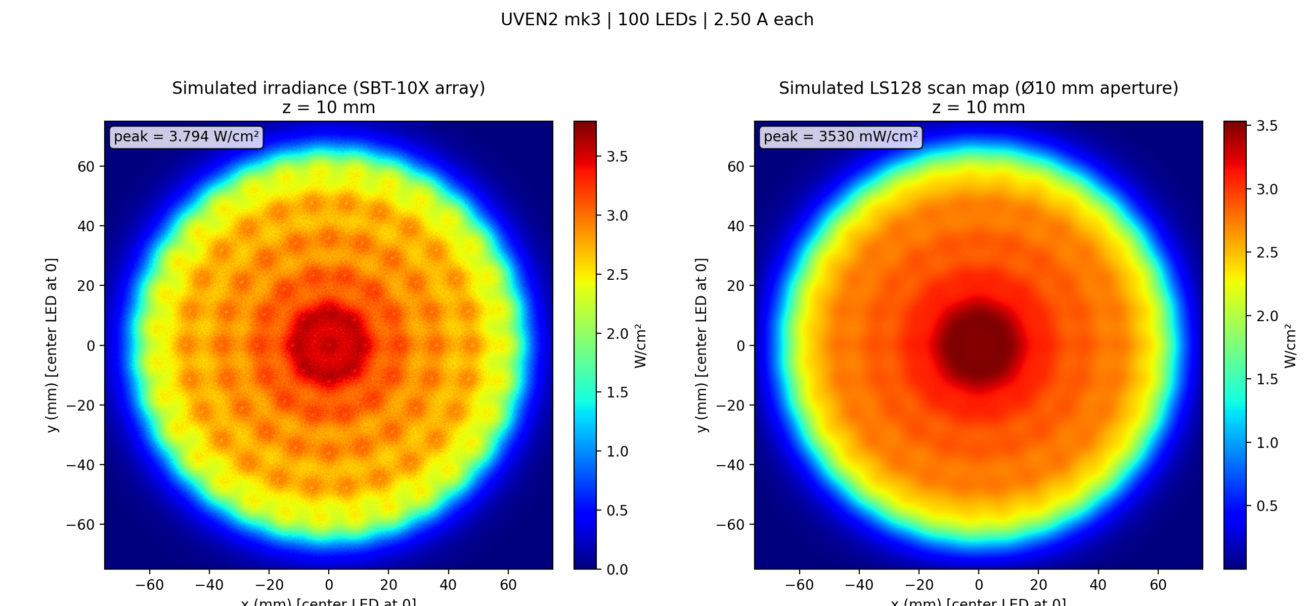
    Luminus provides zemax ray spectrum files for their LEDs. So we were able to simulate the optical power distribution of our LED panel.
    We had somewhat arbitrarily decided on the substrate to be at 10mm distance from the LEDs. Using the simulation this reveiled hot spots.

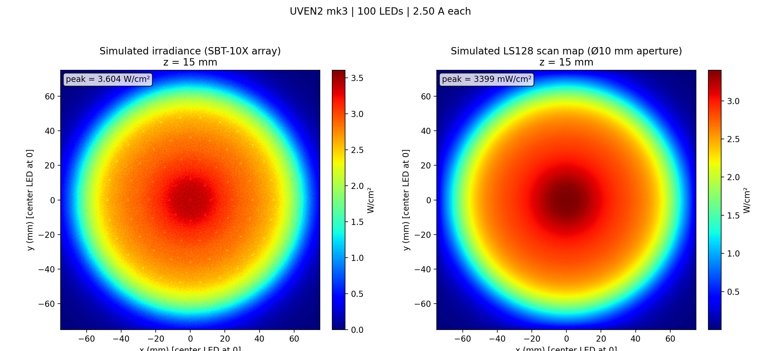
    Simulating at increments of 1mm, a much more homogenous optical power distribution should be at 15mm.

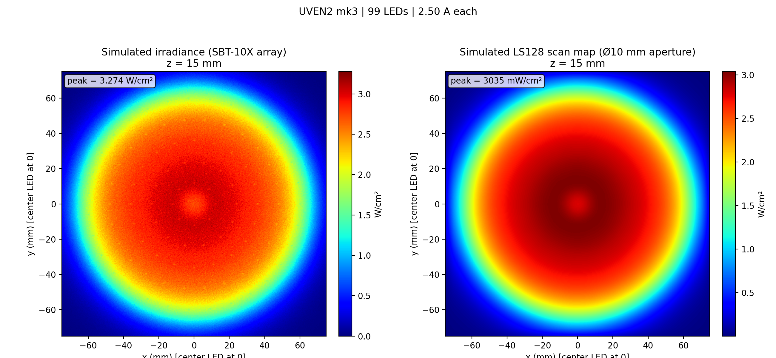
    The center still showed a hot region. Removing the center LED would fix this to some extend.

    So we decided to implement these changes in the final design. In CAD we moved the entire LED panel 5 more mm away from the substrate plane. When ordering the LED panel, one should mark the center LED as do not assemble.

  • LED panel performance

    Simon Trendel • 01/05/2026 at 20:18 • 0 comments

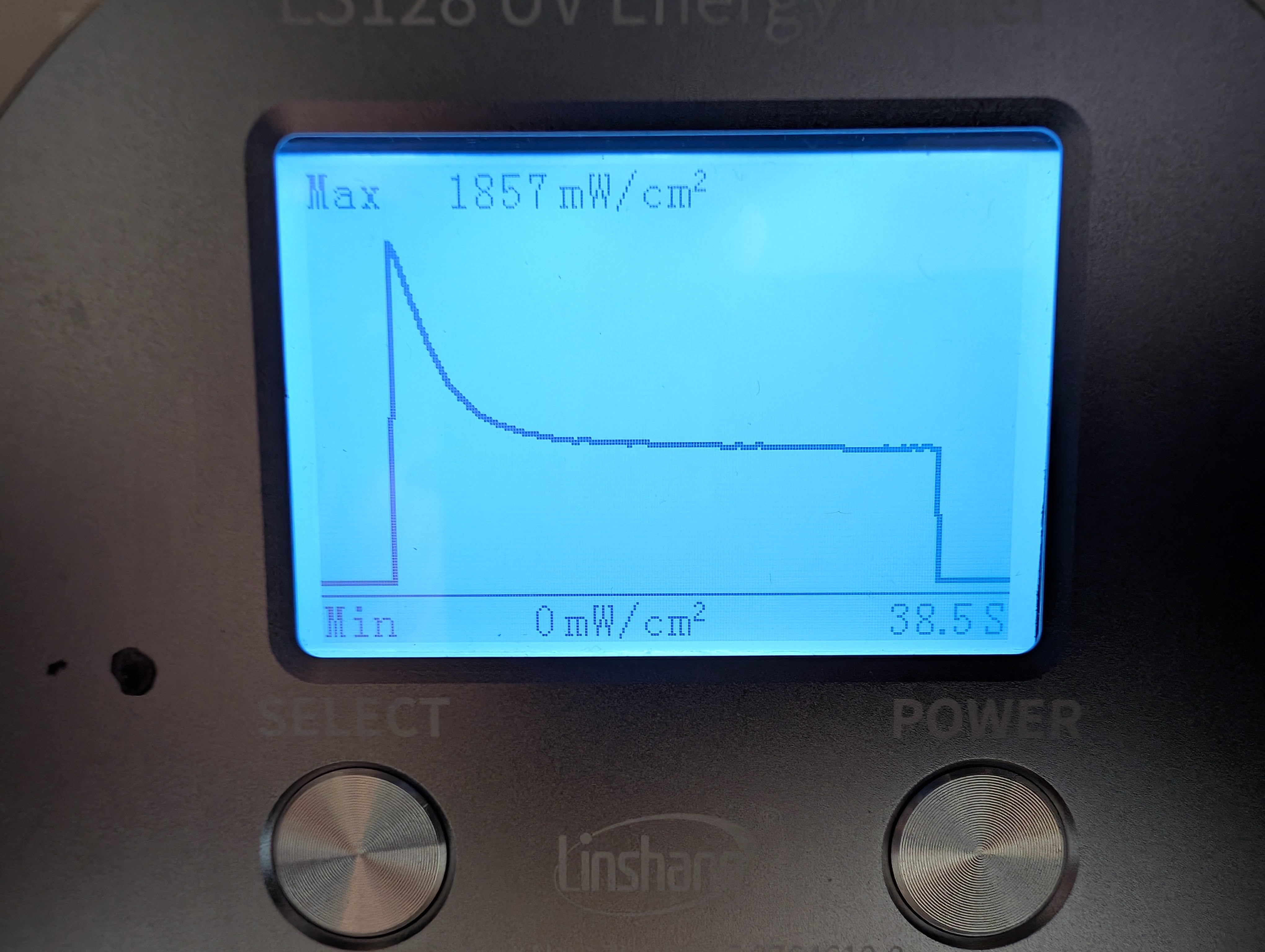
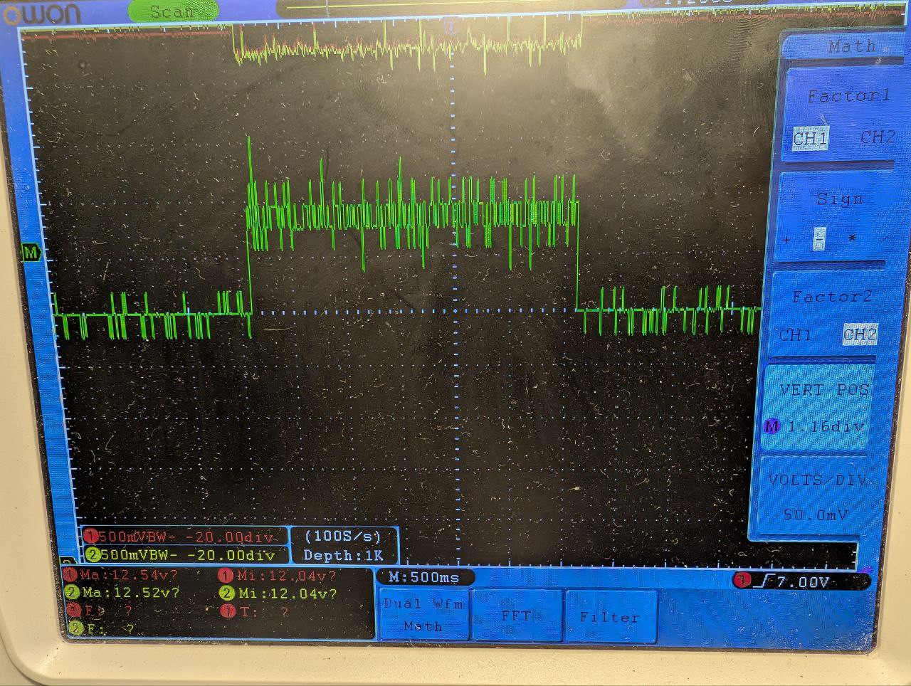
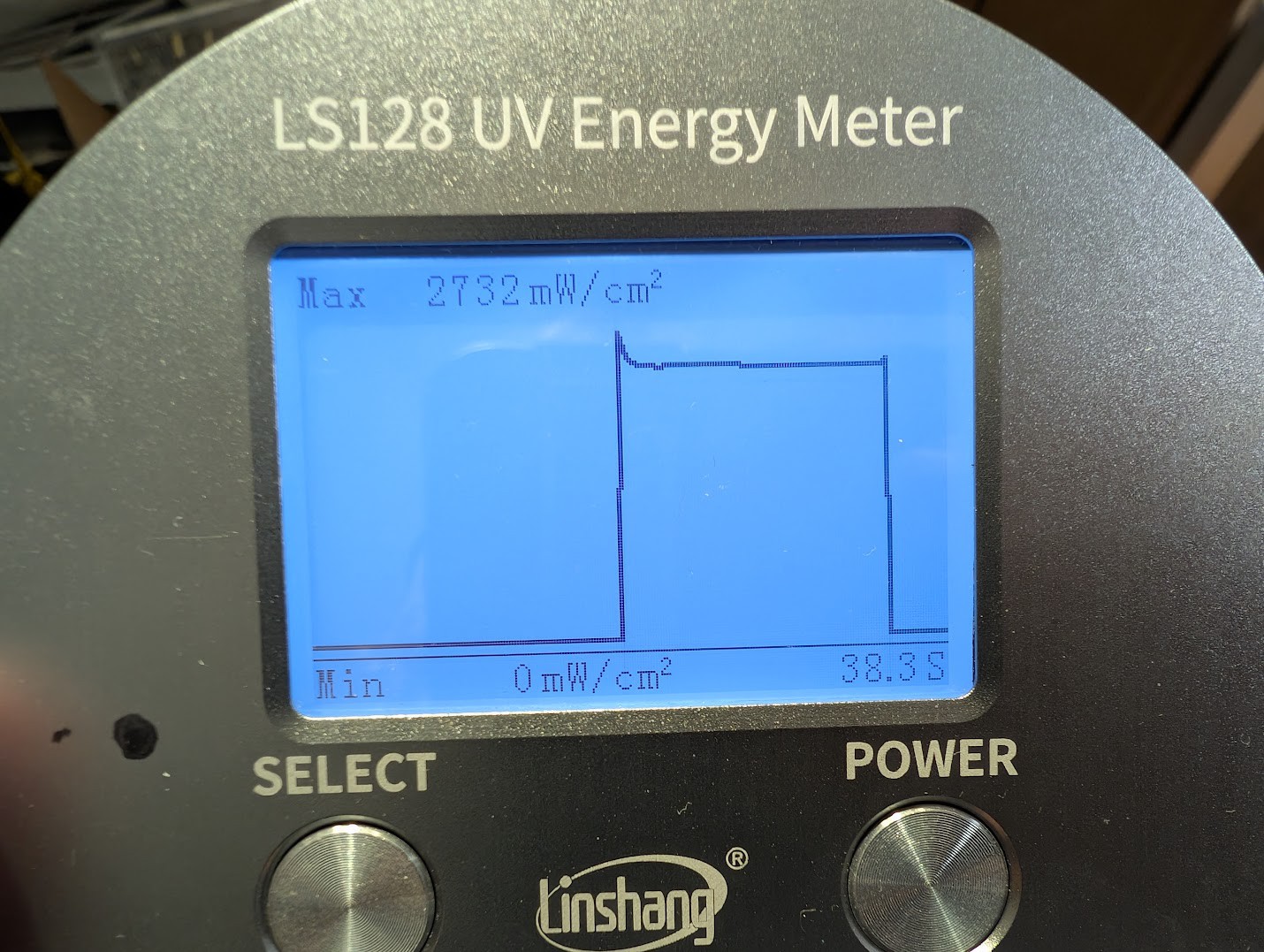
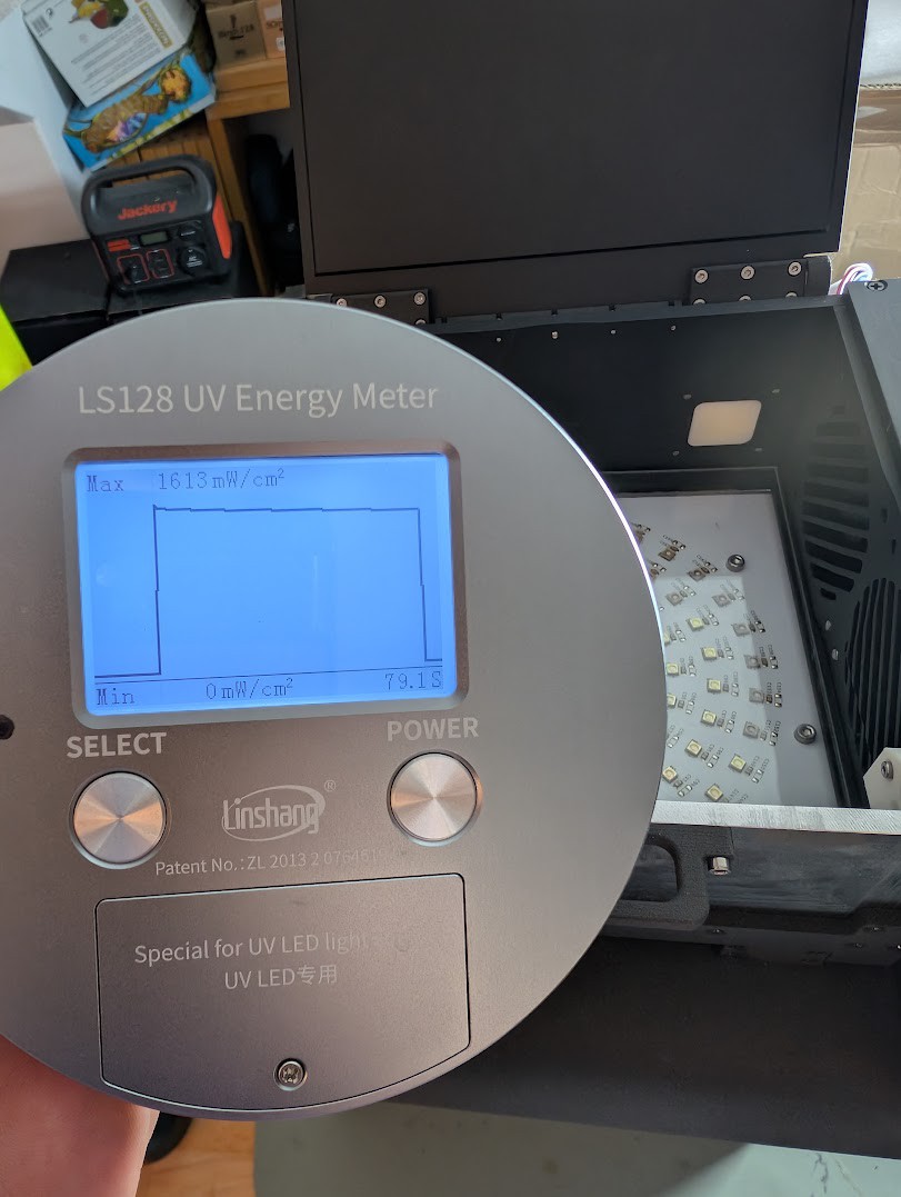
    We tested the fully assembled device and unfortunately the optical power dropped to 40% after a short duration.

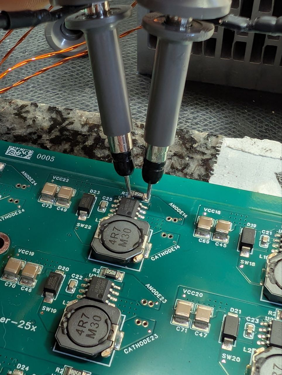
    This was unacceptable and we needed to investigate. Probing the voltage across the current sense resistor showed the driver was working correctly.

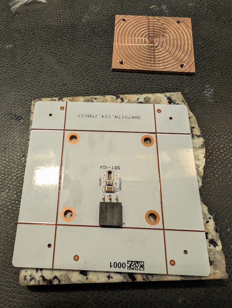
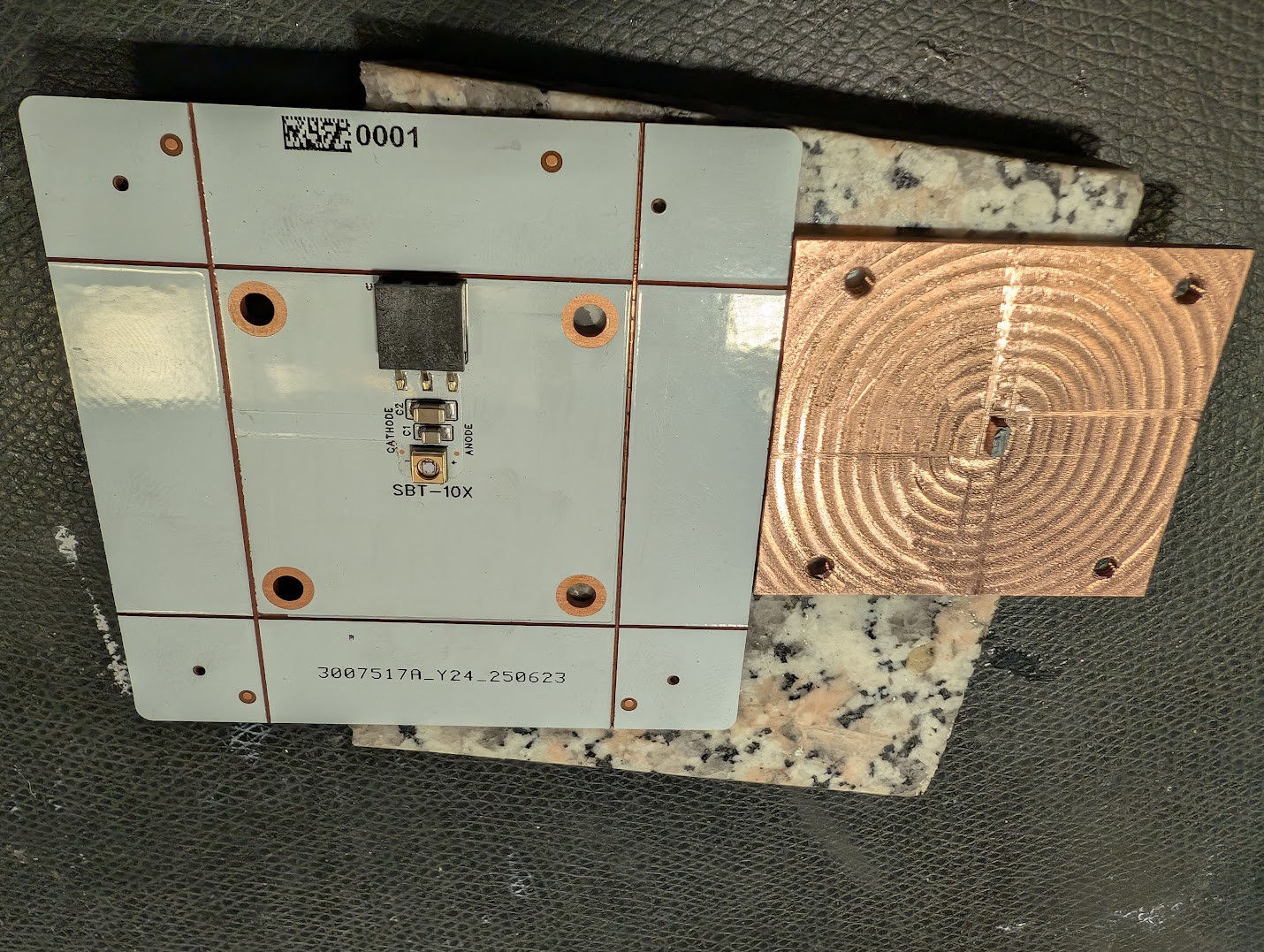
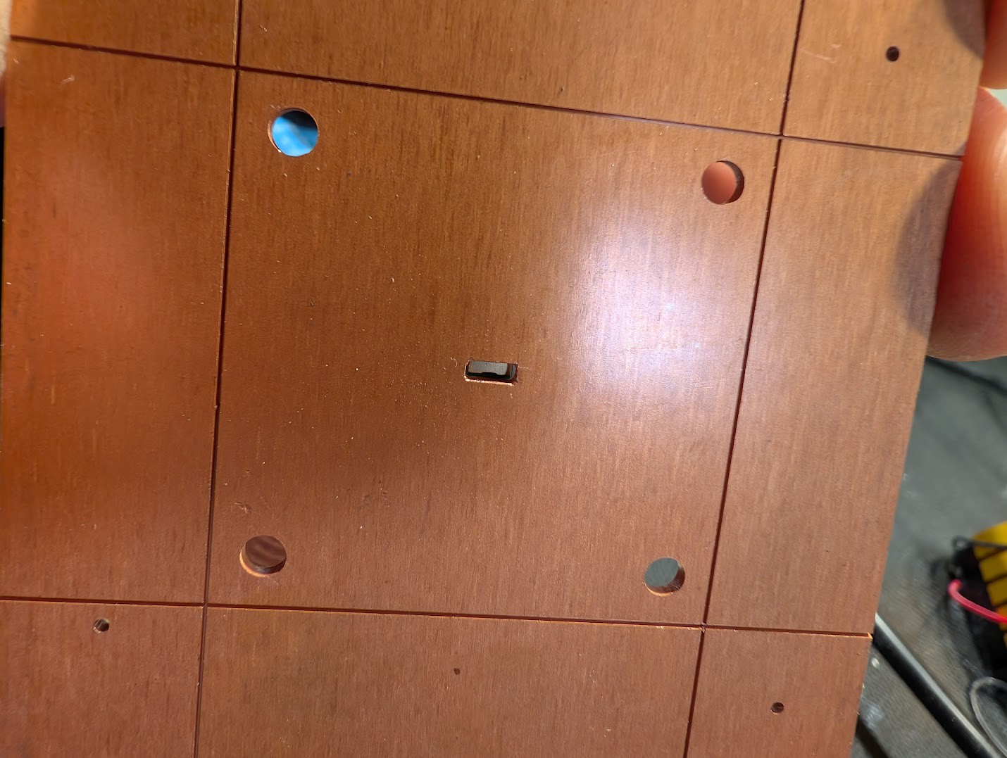
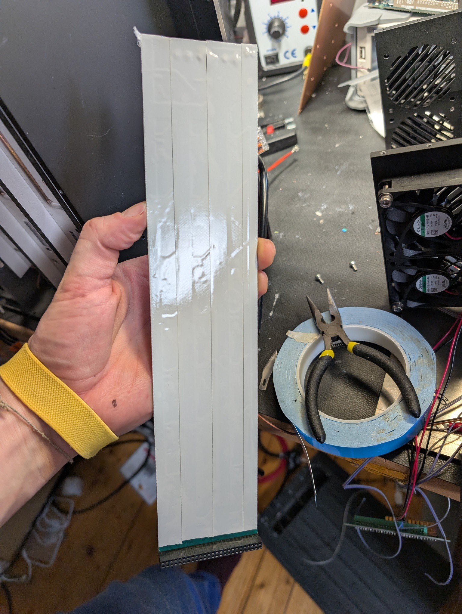
    The only possible reason seemed to be a thermal problem. When ordering the LED panel as copper base PCB, one needs to define thermal heat sinks. These are areas of the PCB that are full copper and can provide excellent thermal dissipation. Unfortunately in this version, we had not defined the heat sink pad of the LED as direct heat sink. To test this hypothesis we modified one of the test PCBs by milling out the heat sink pad and mounting a fitting copper heat sink into this slot.

    And indeed, the optical power now was stable.

    So we ordered a new version of the LED panel. The white areas in the layout are direct heat sinks.

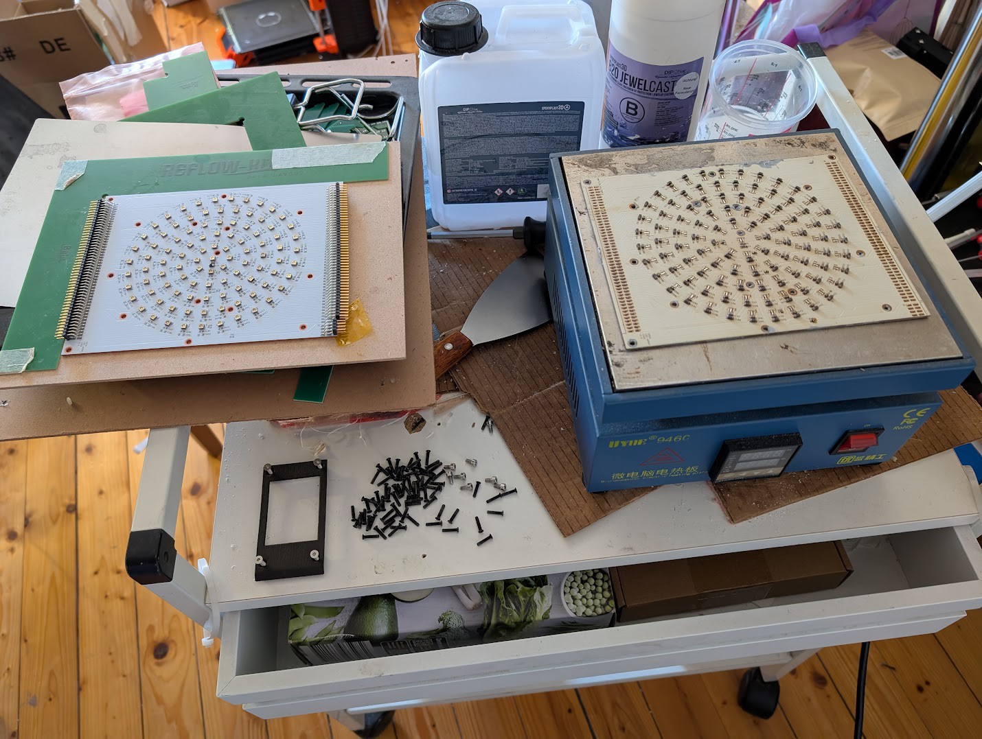
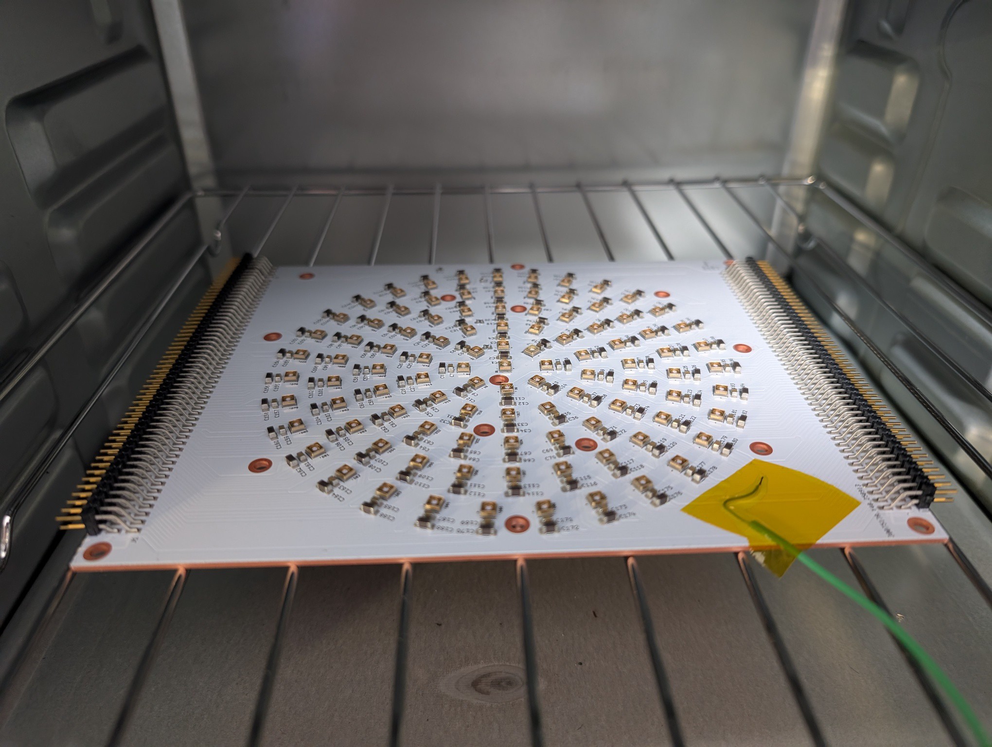
    We then desoldered all 100 LEDs and resoldered them to the new panel.

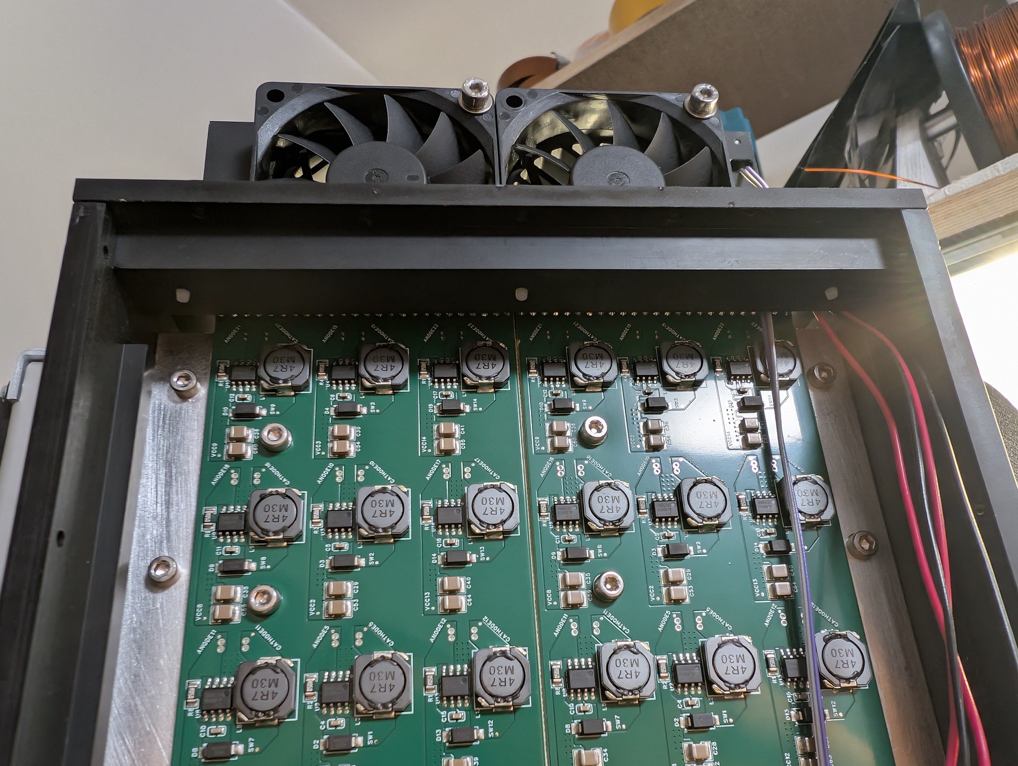
    And finally the test in the fully reassembled device showed much more stable optical power output.

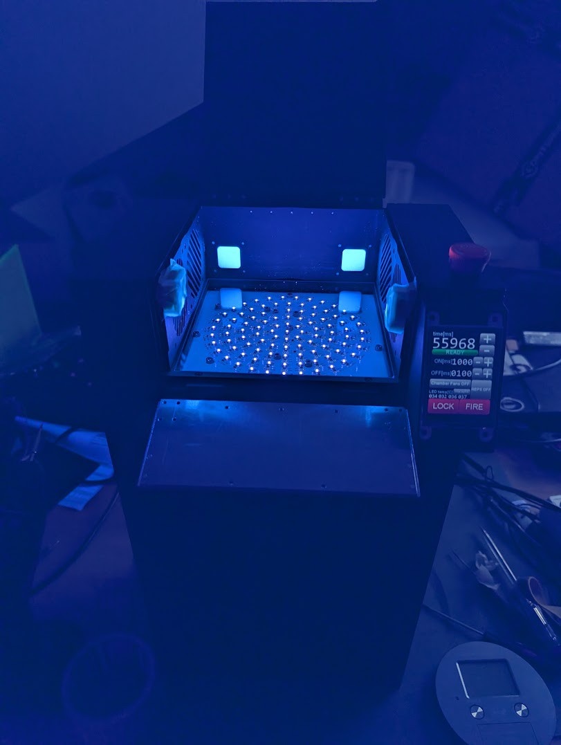
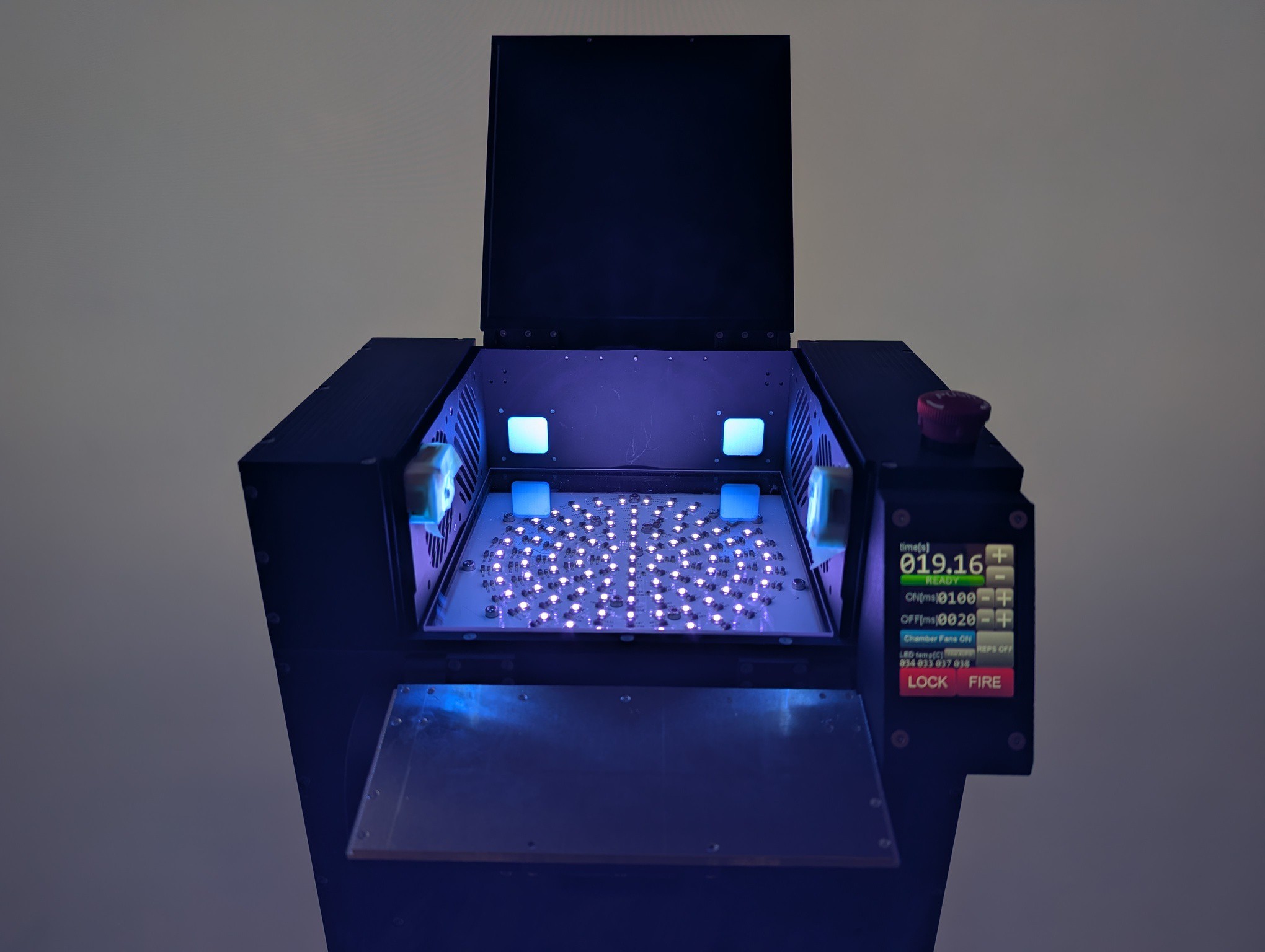
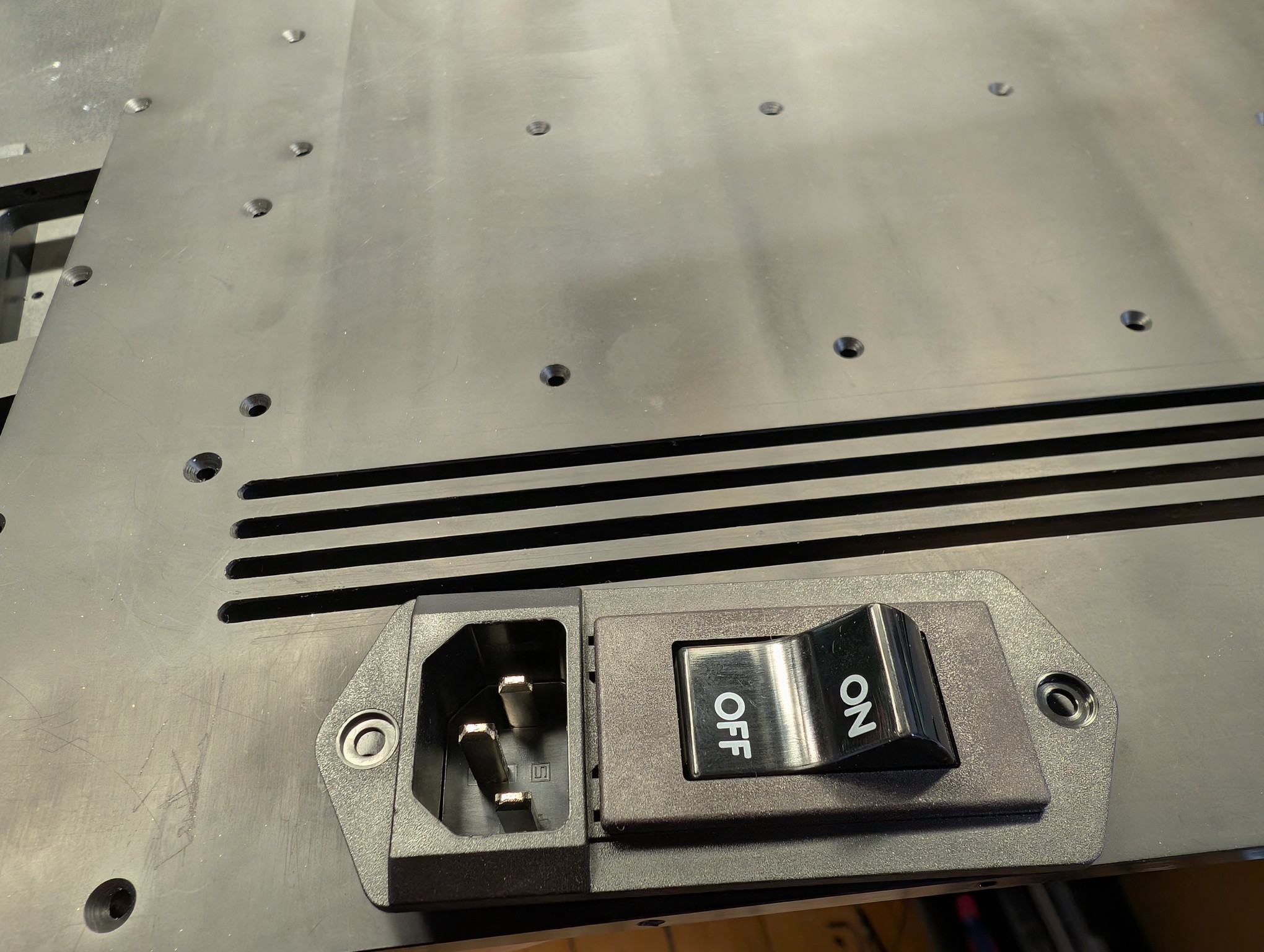
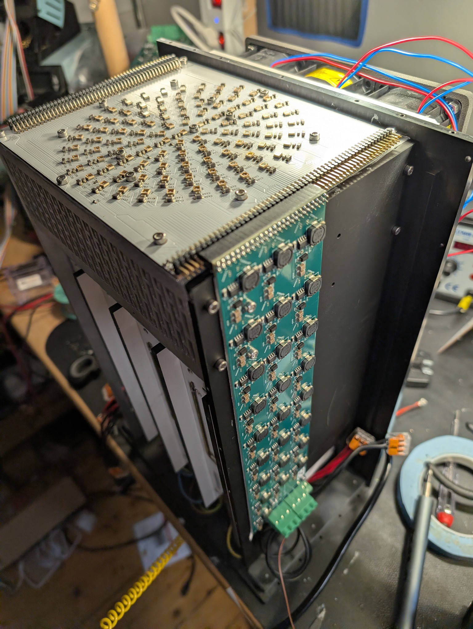
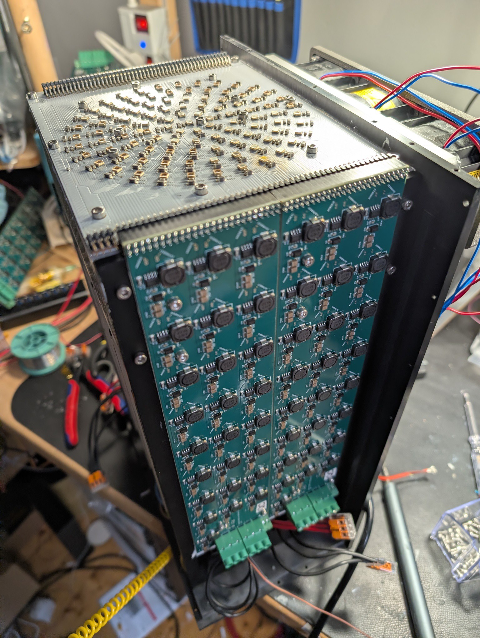
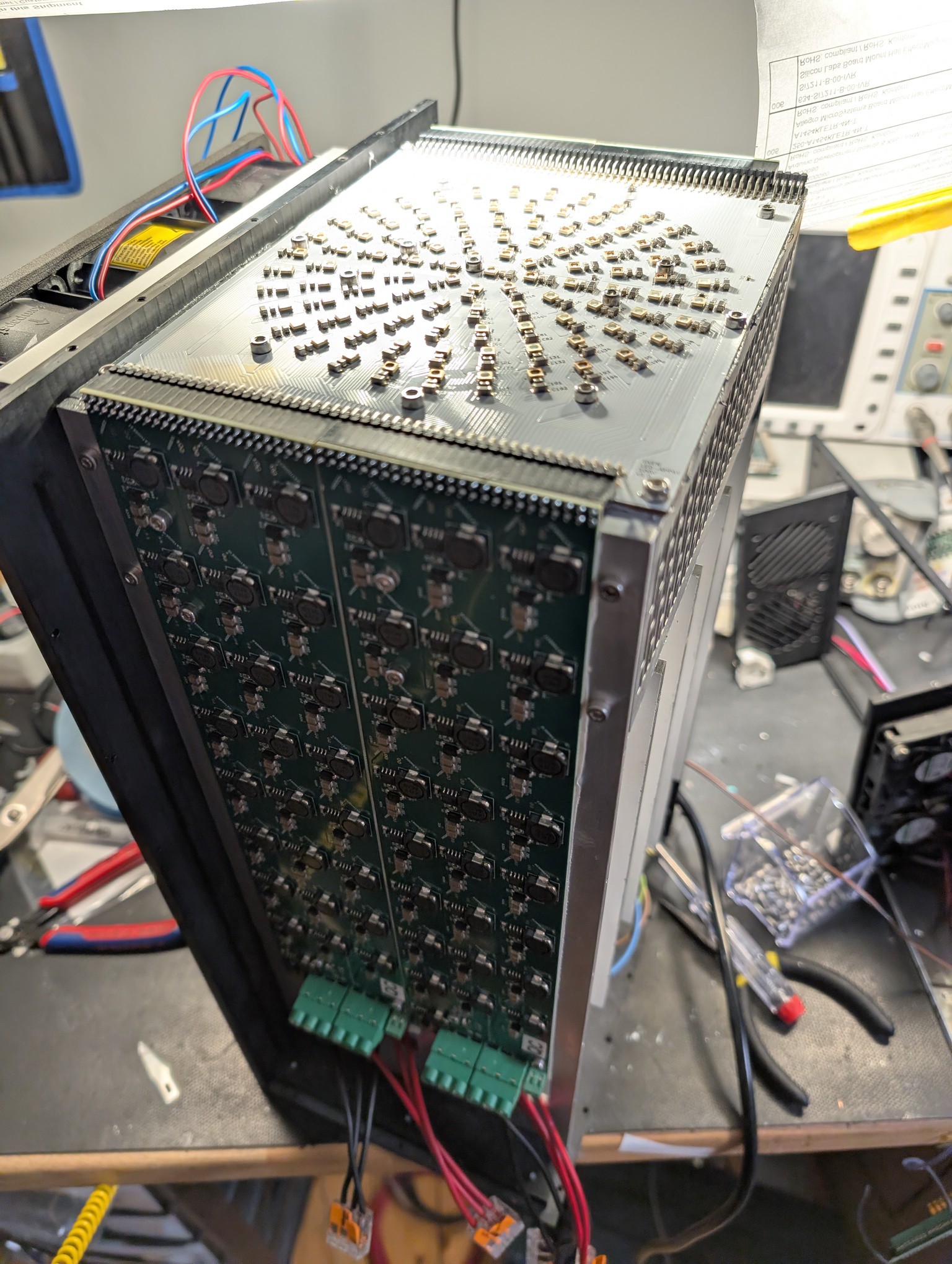
  • Final assembly #3 - light it up

    Simon Trendel • 11/06/2025 at 12:46 • 0 comments

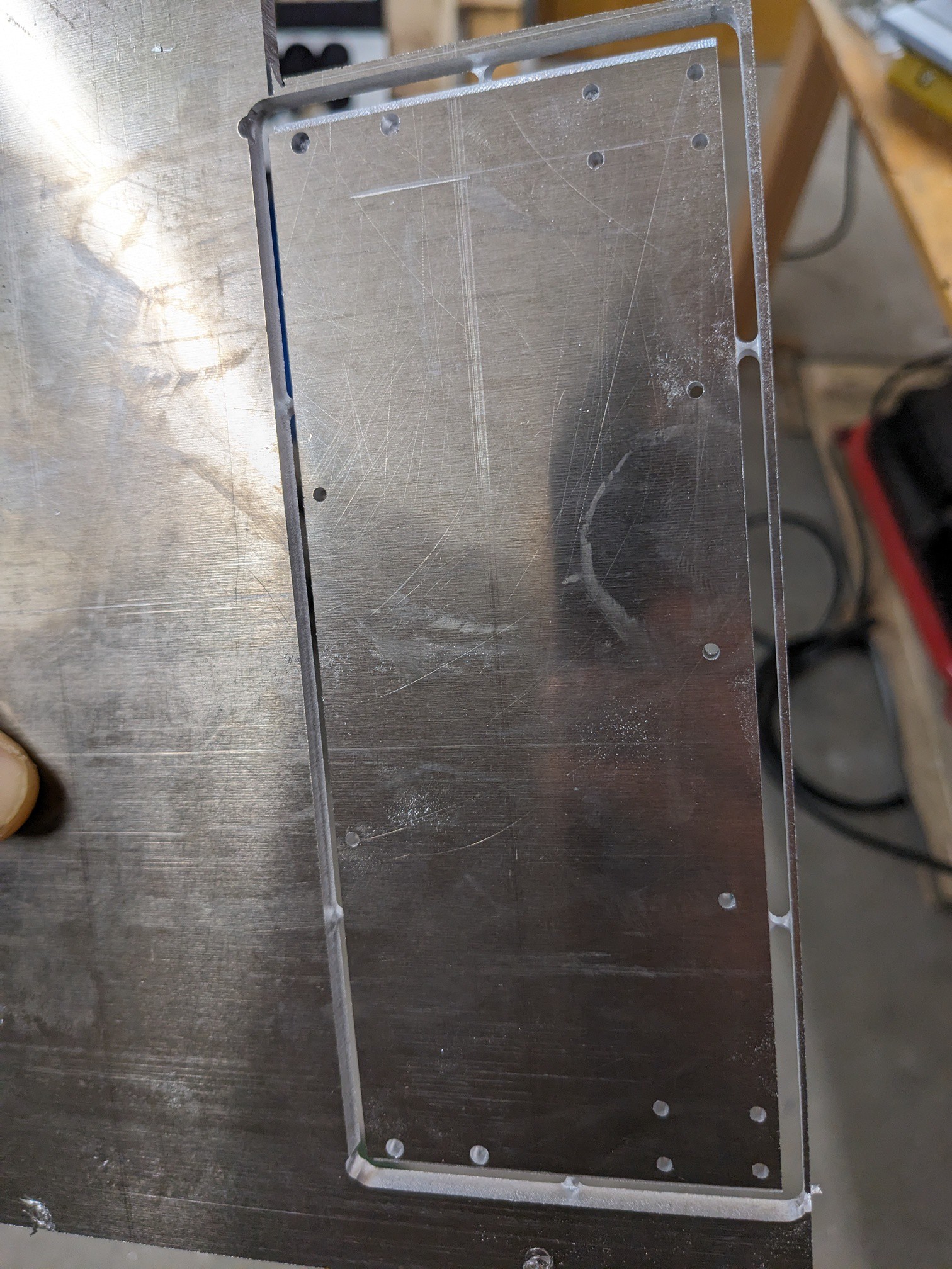
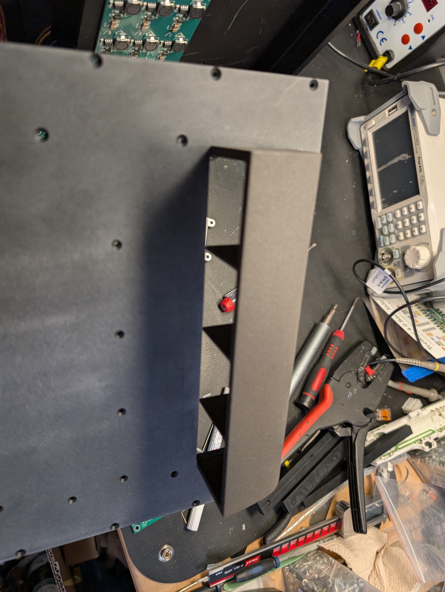
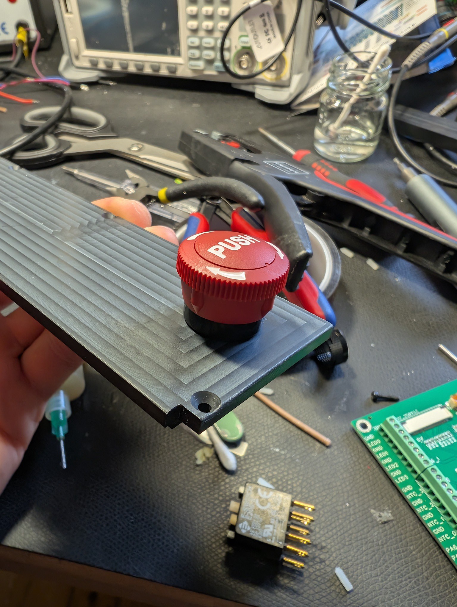
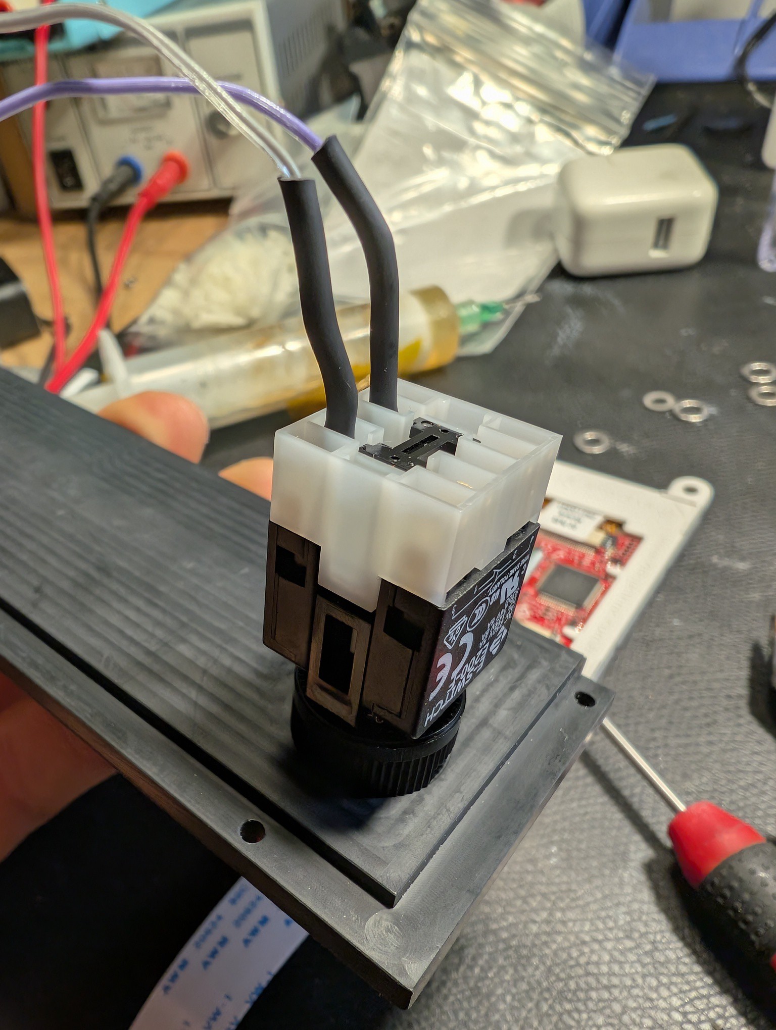
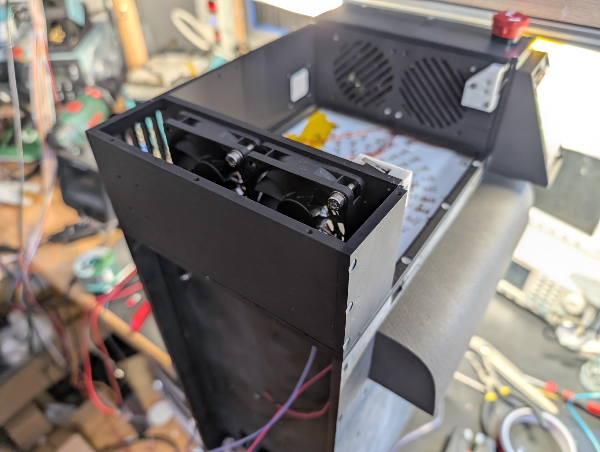
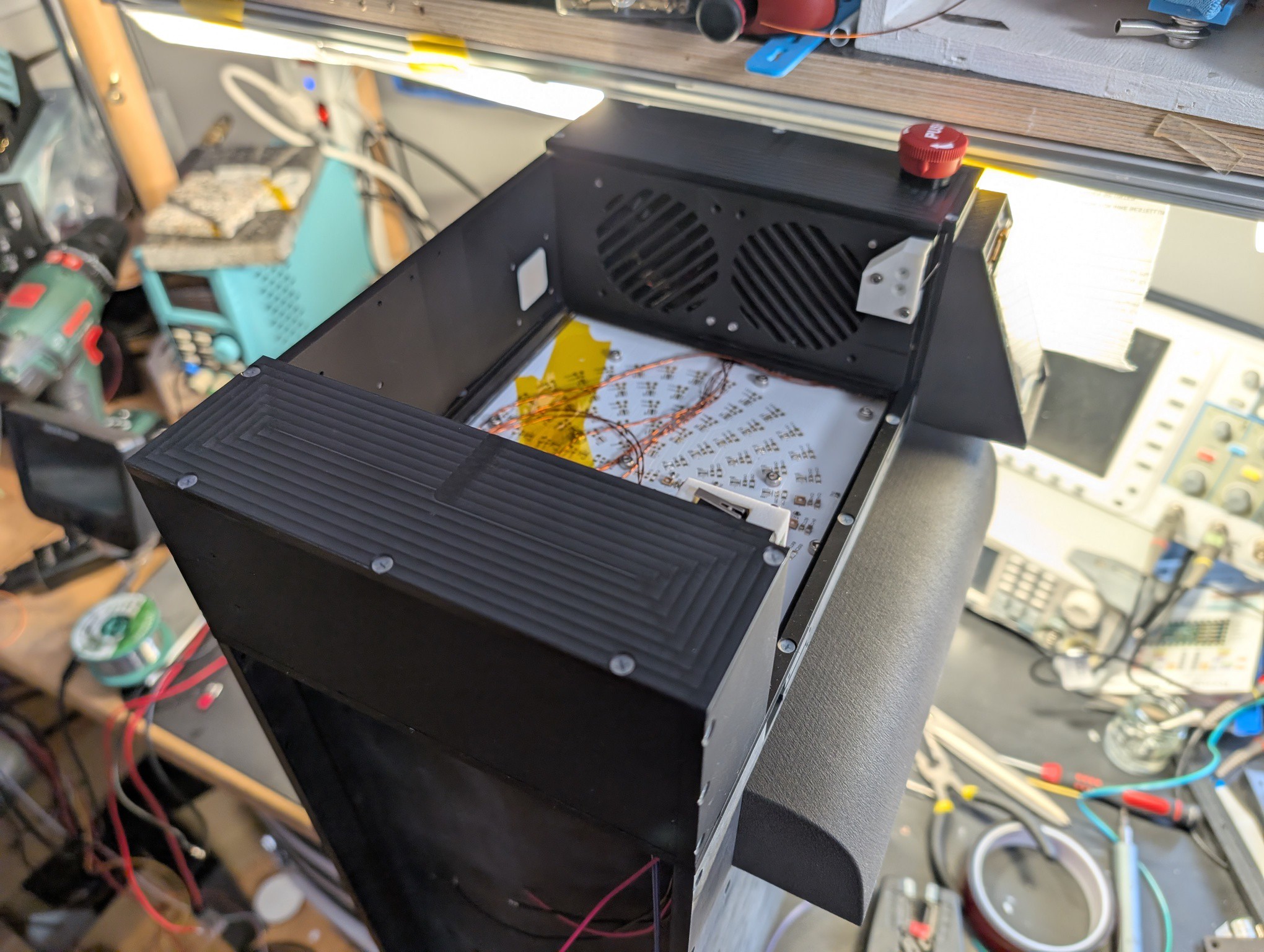
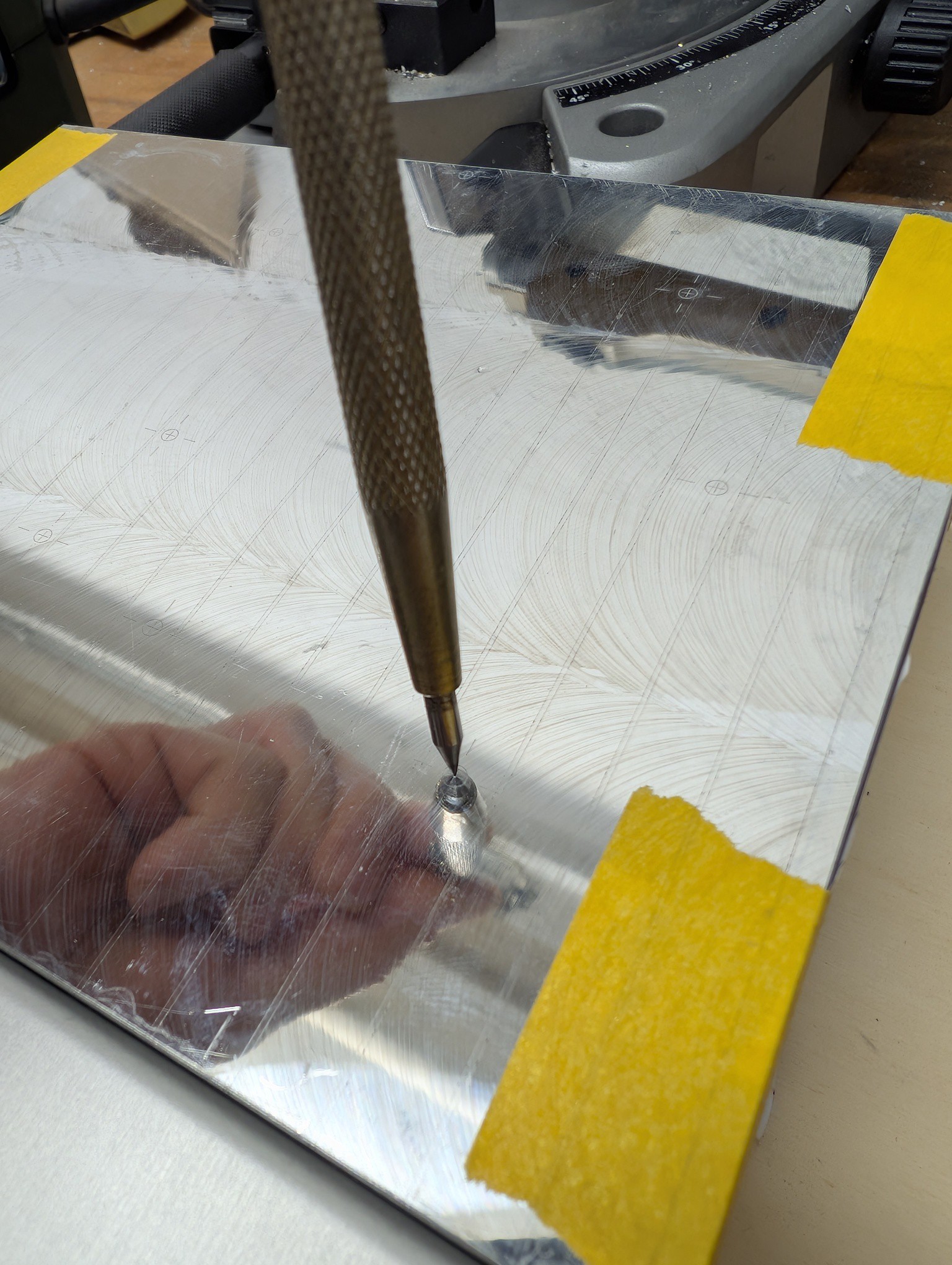
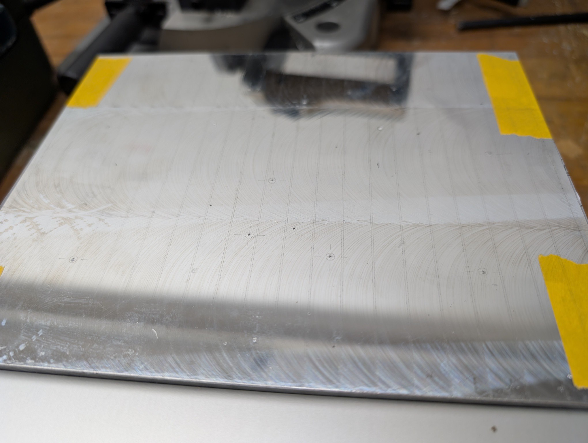
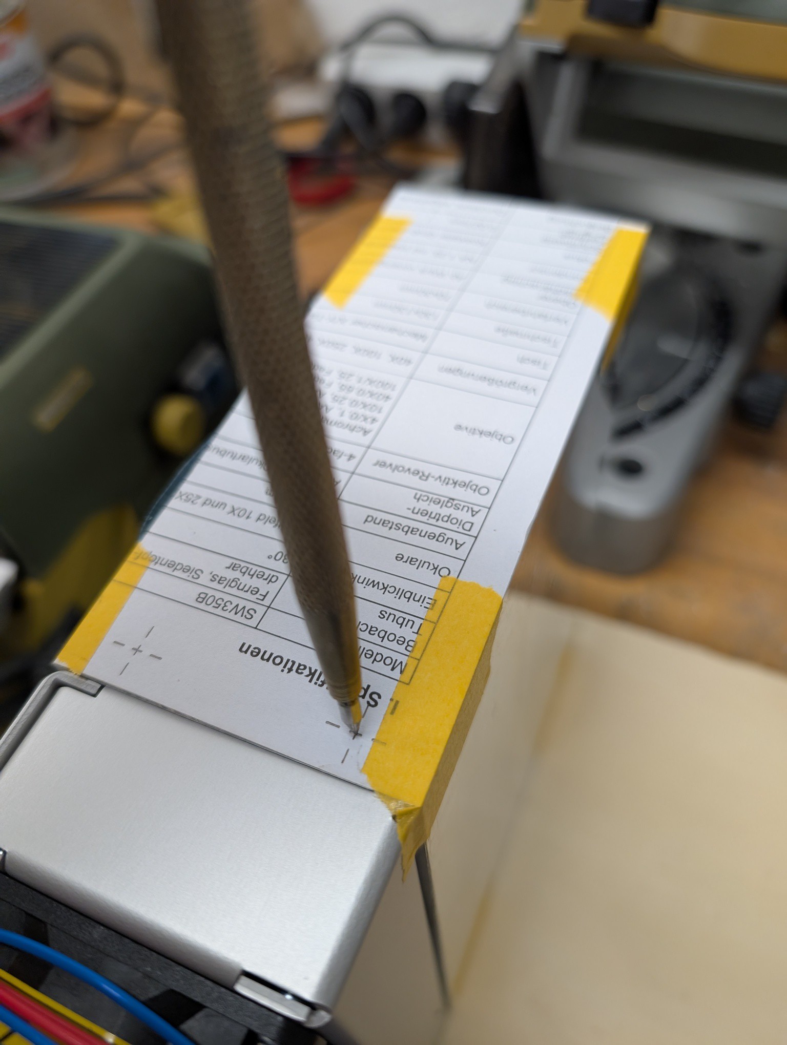
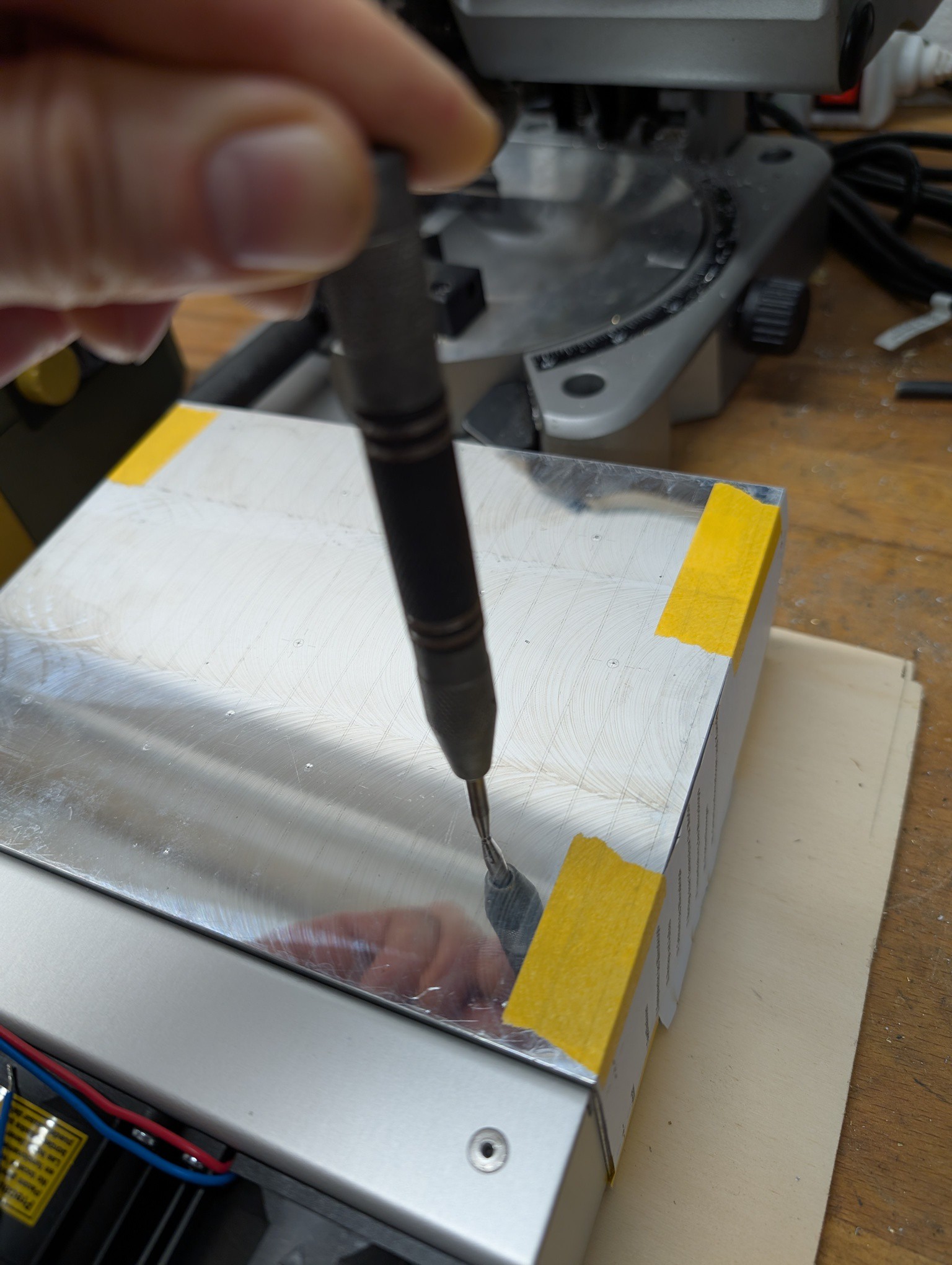
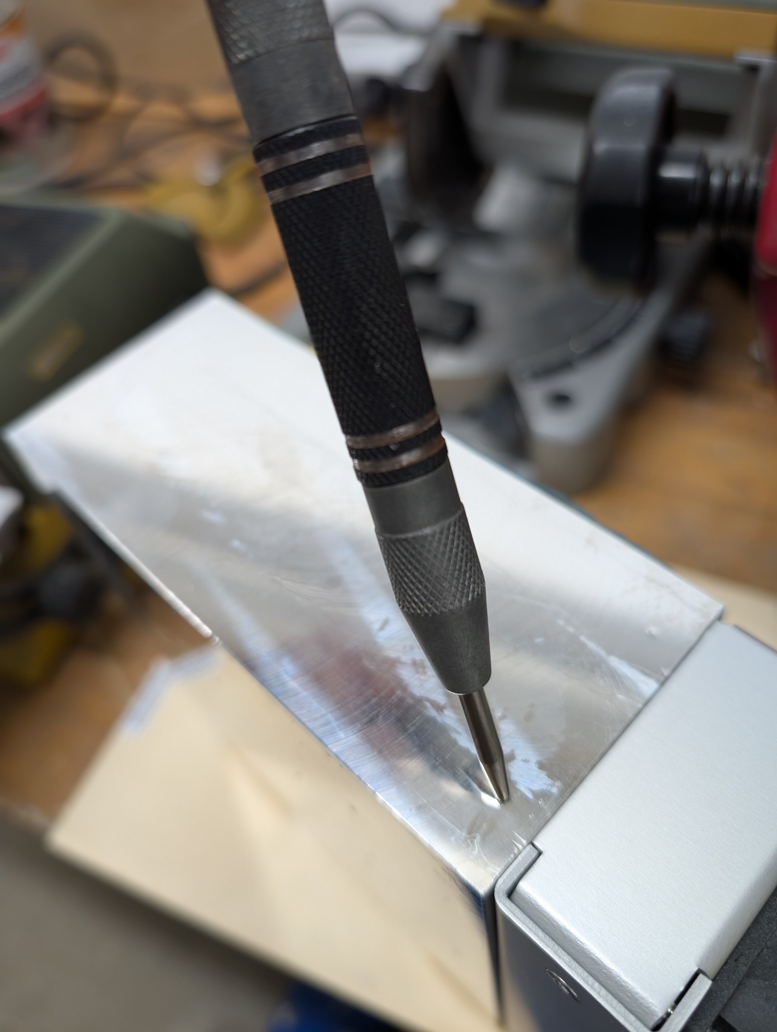
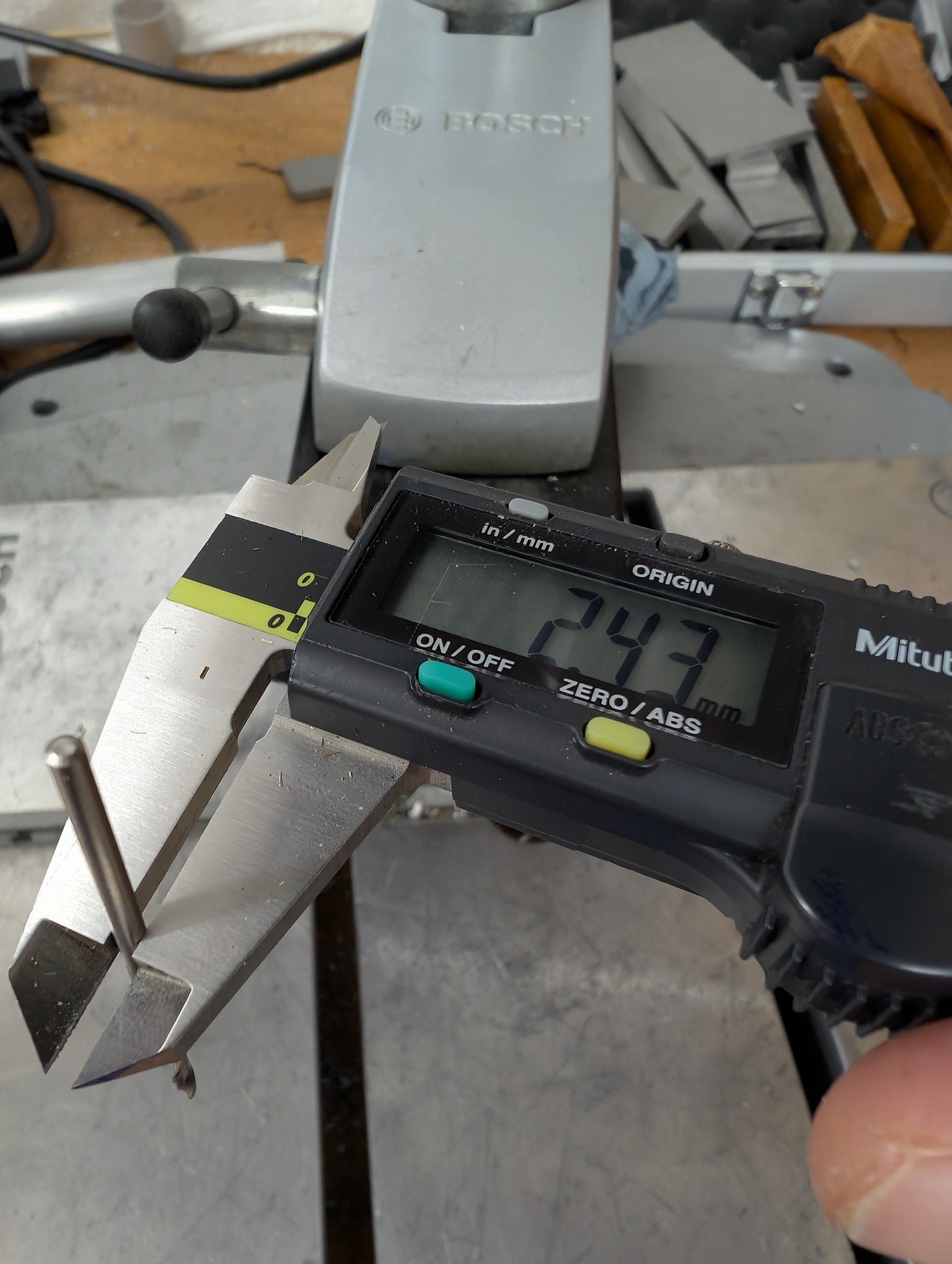
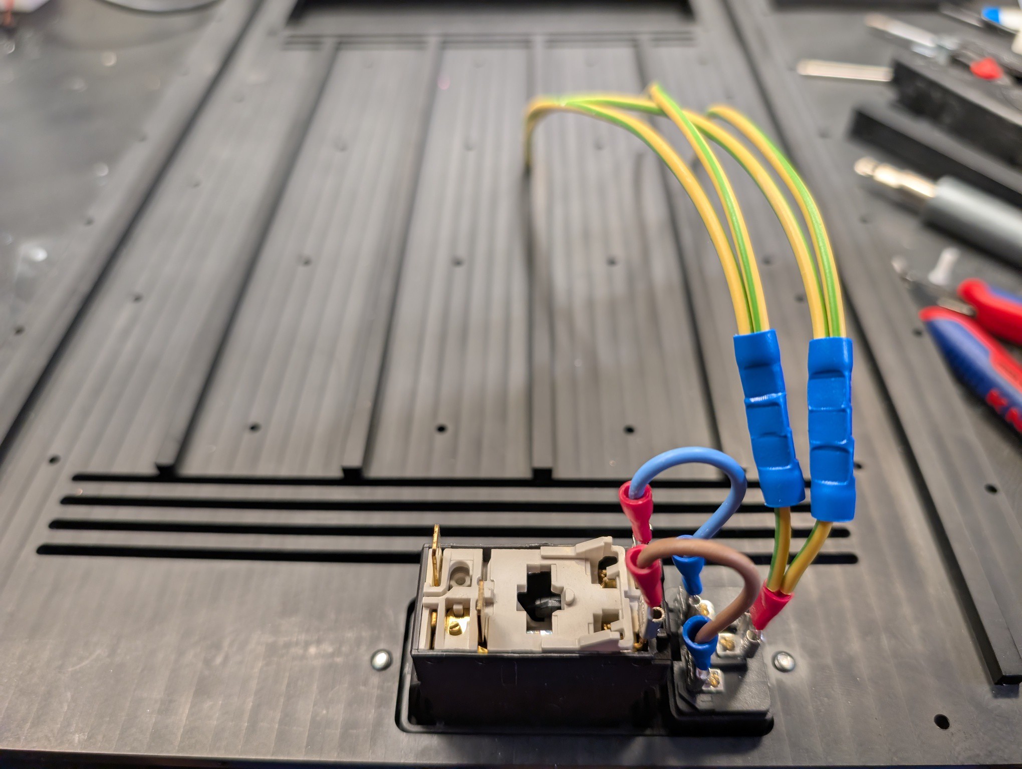
    I forgot to order the front lid, so I machined it in my workshop

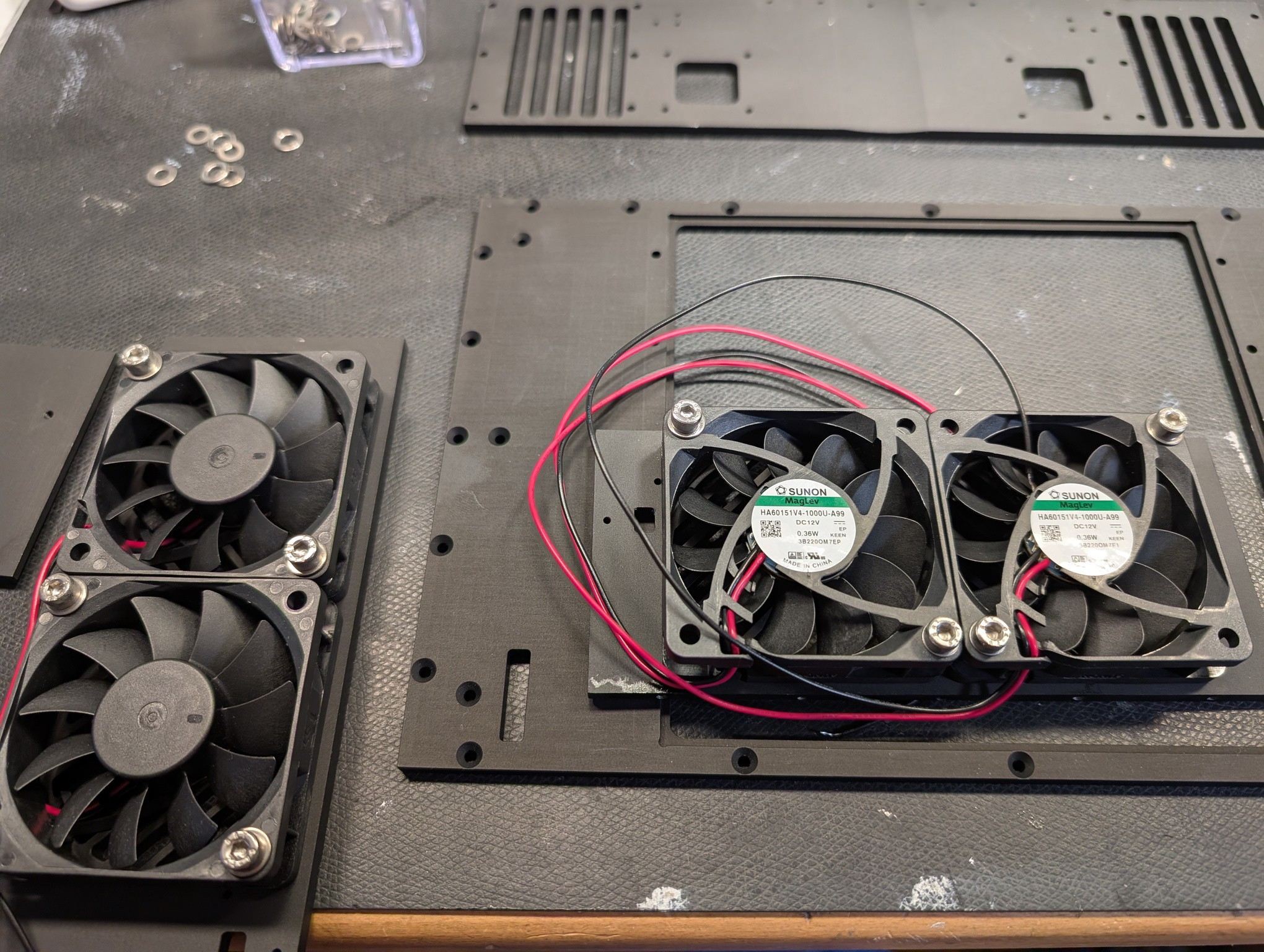
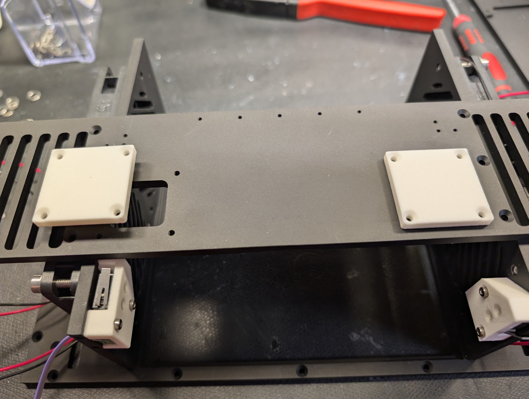
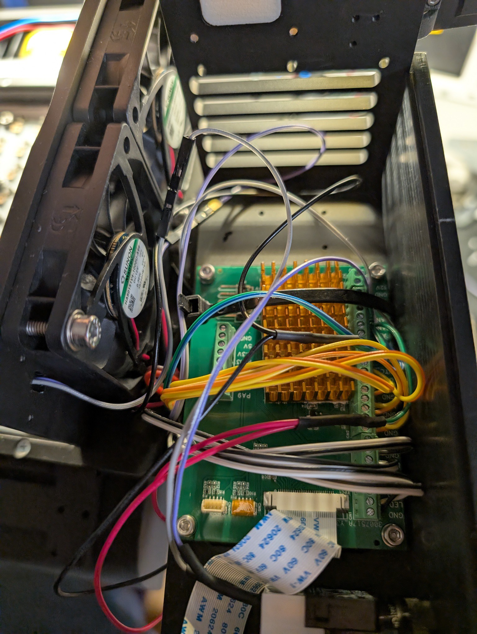
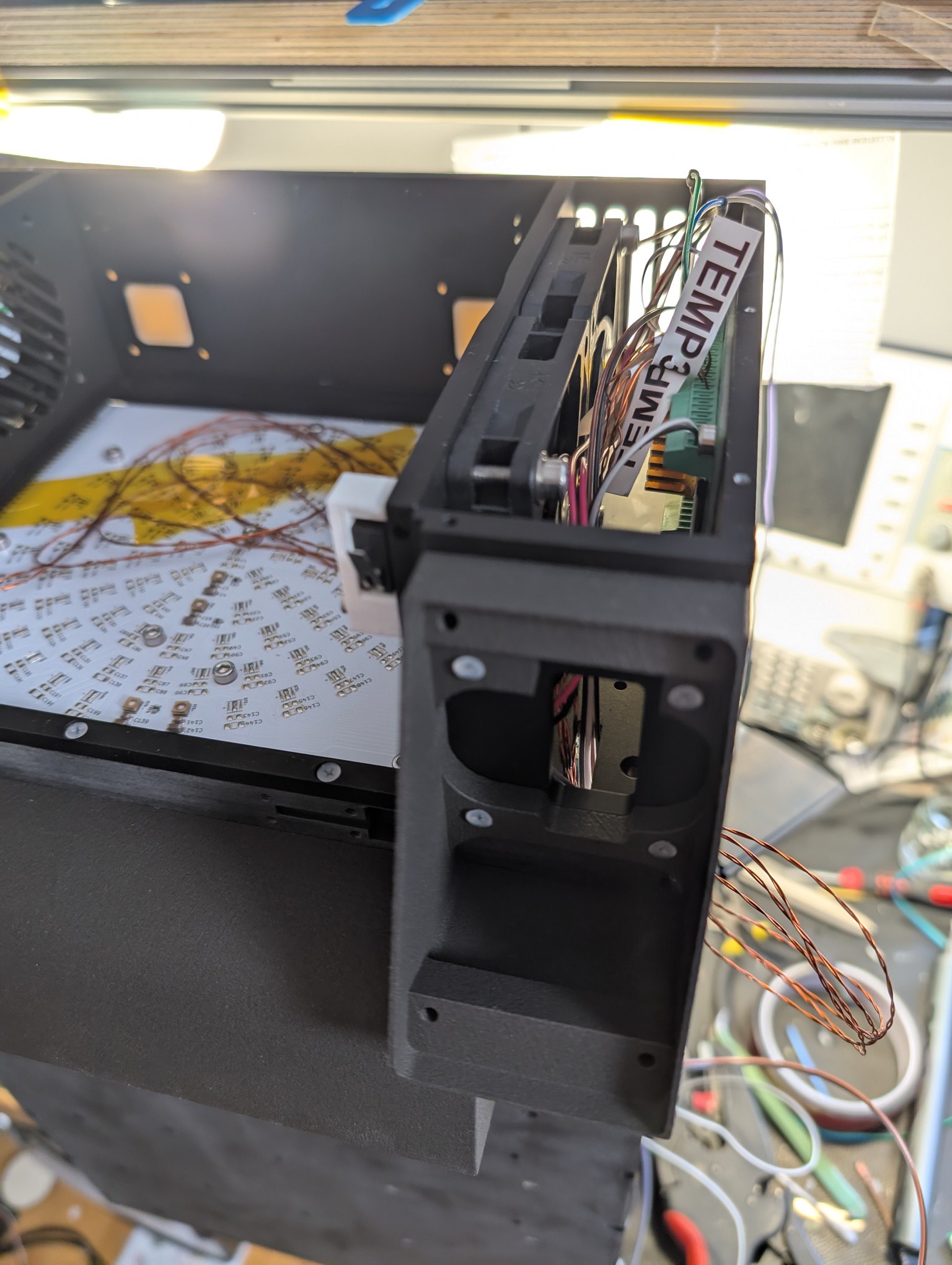
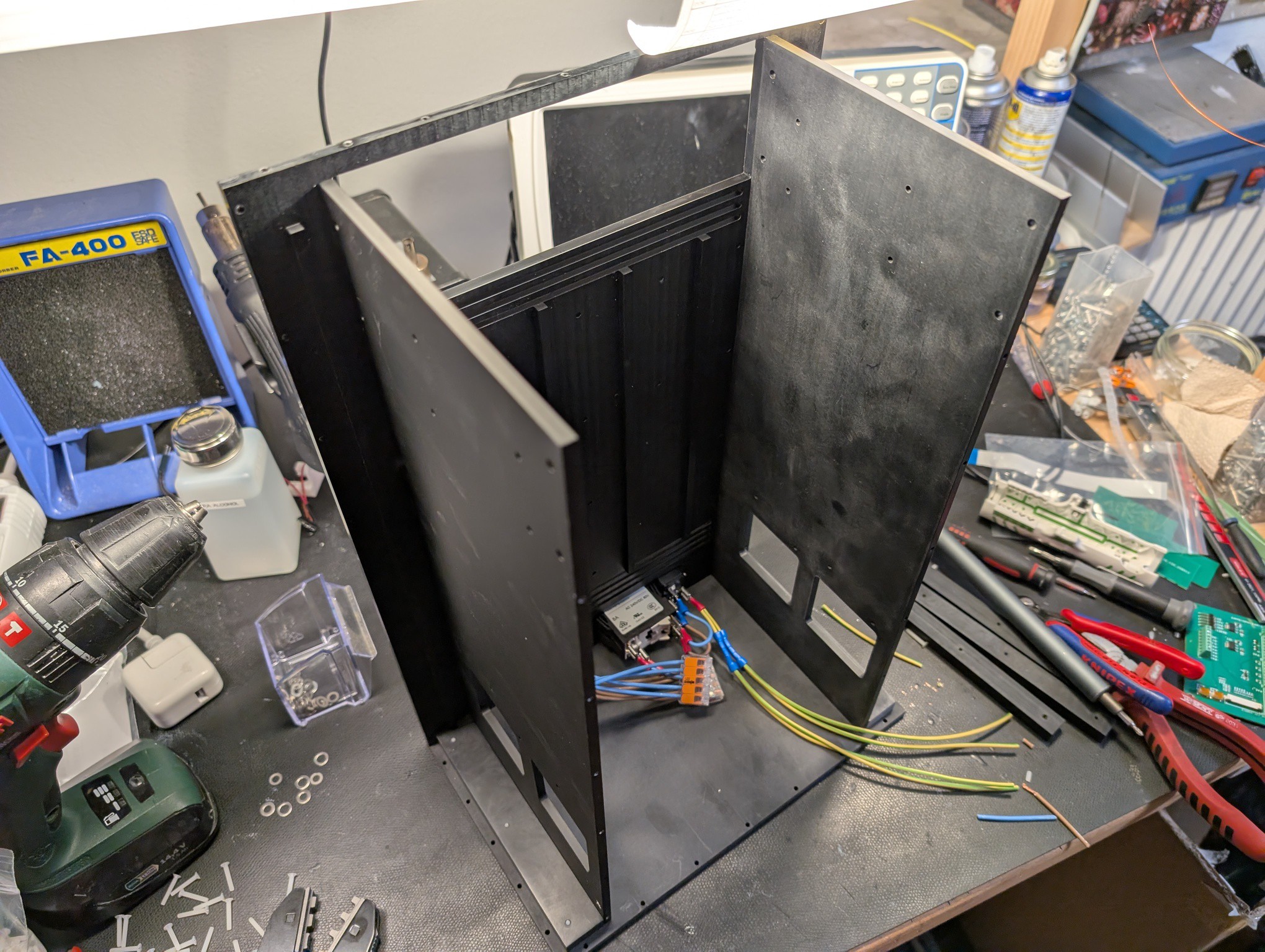
  • Final assembly #2 - put it all together

    Simon Trendel • 11/06/2025 at 12:39 • 0 comments

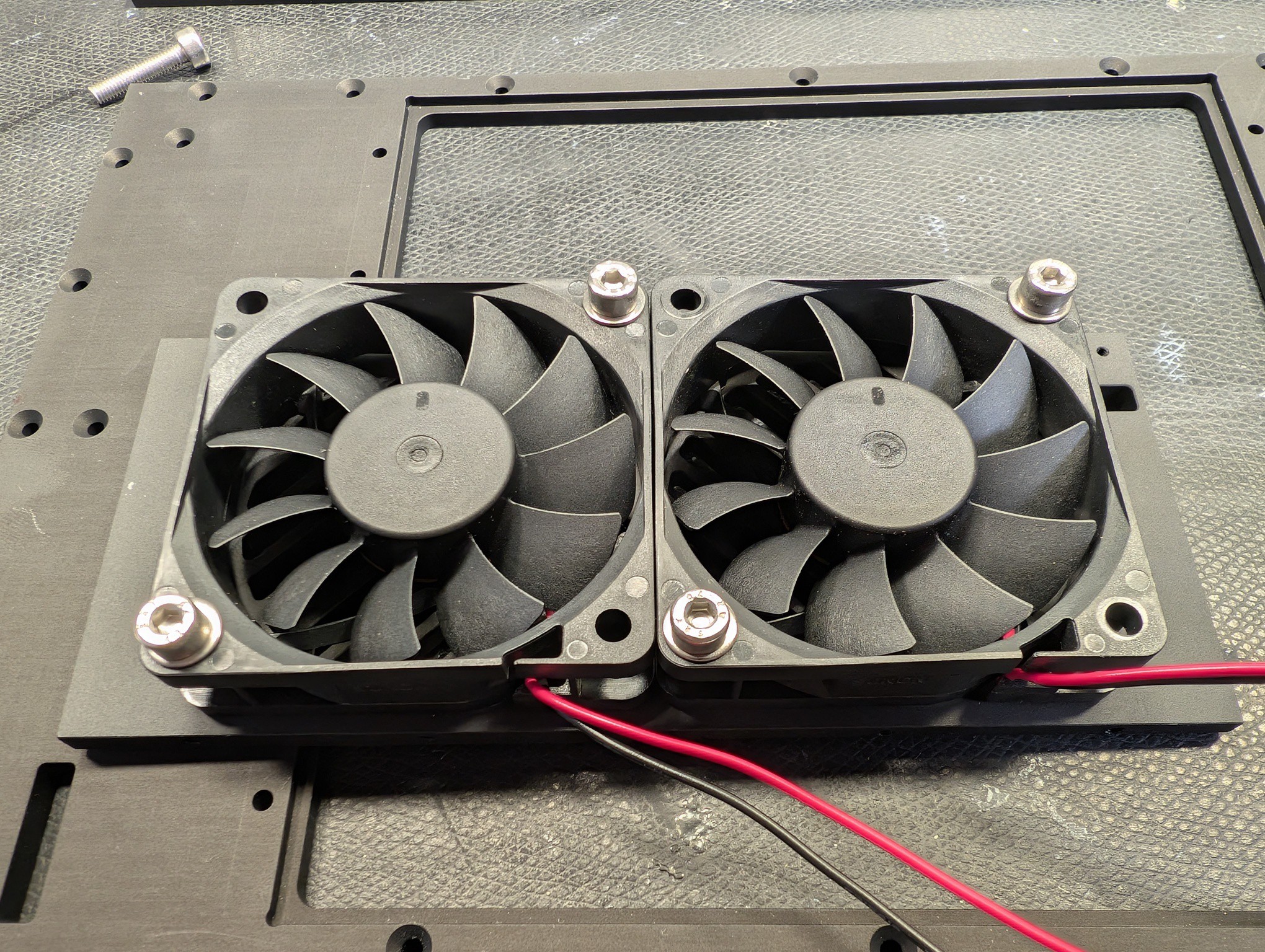
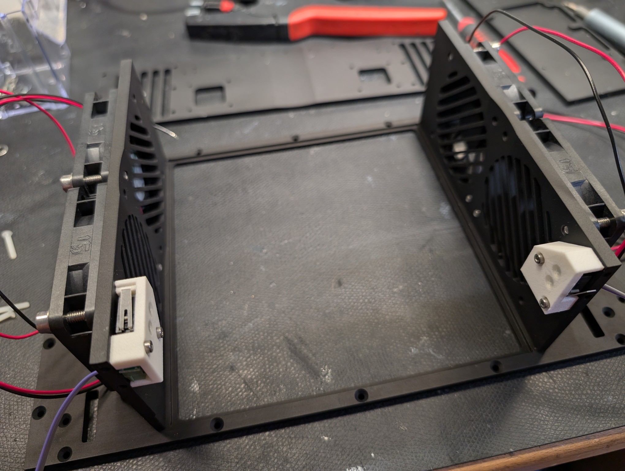
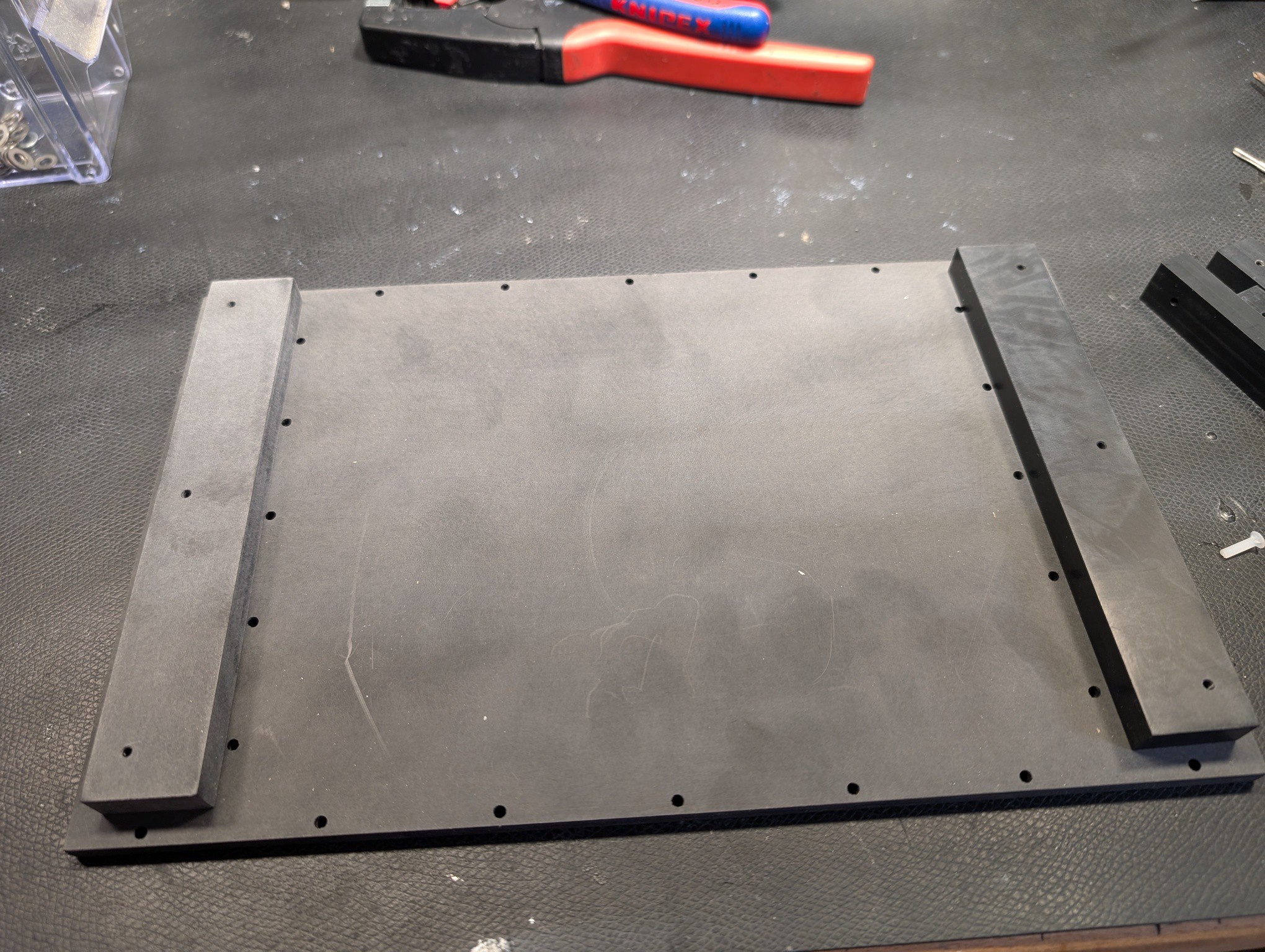
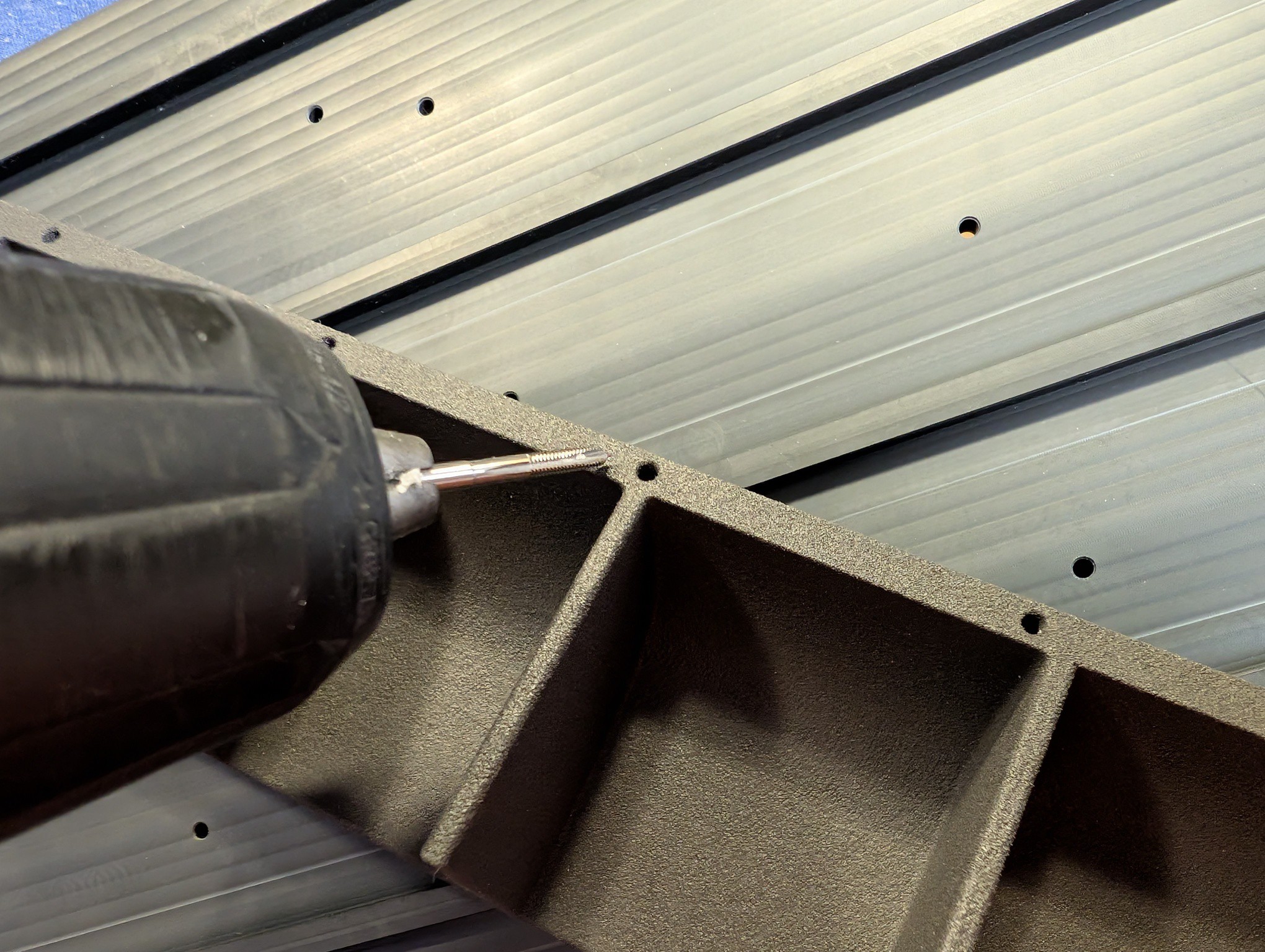
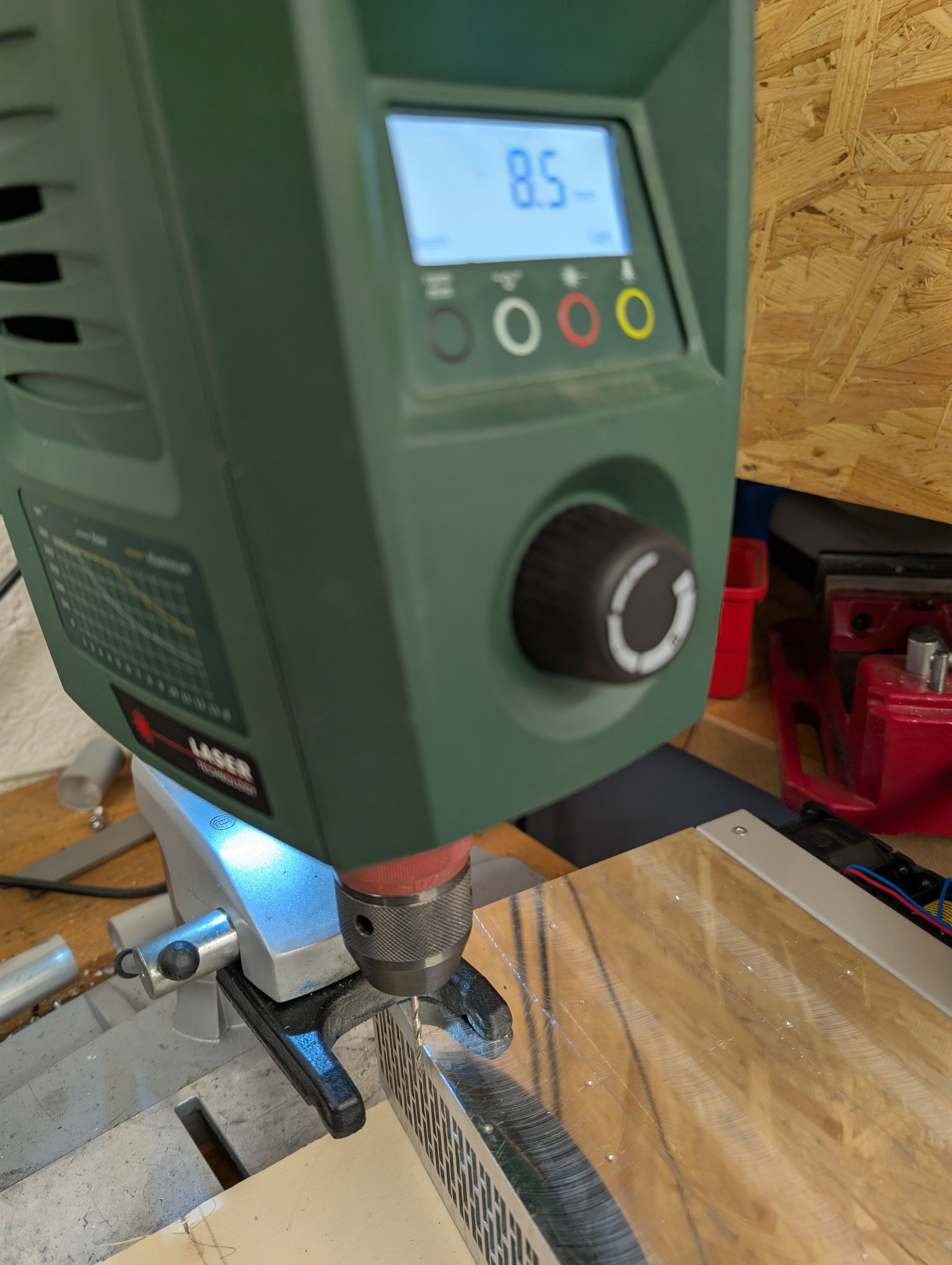
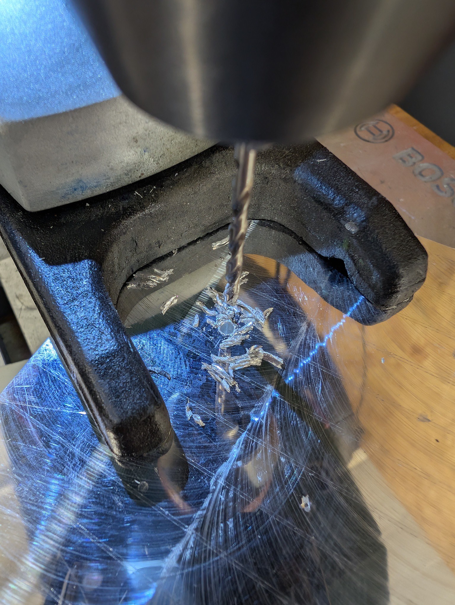
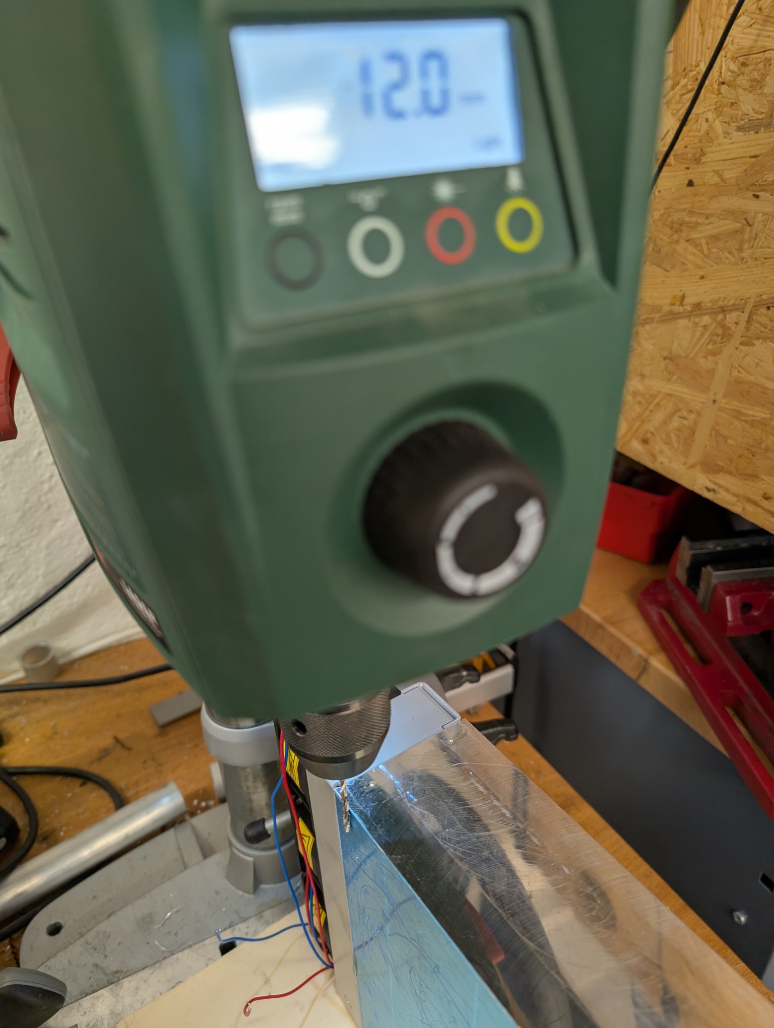
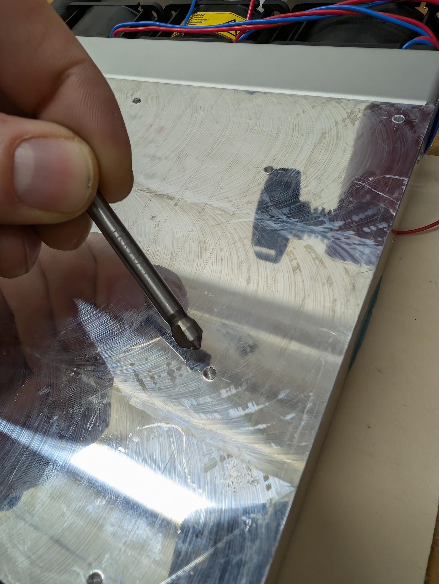
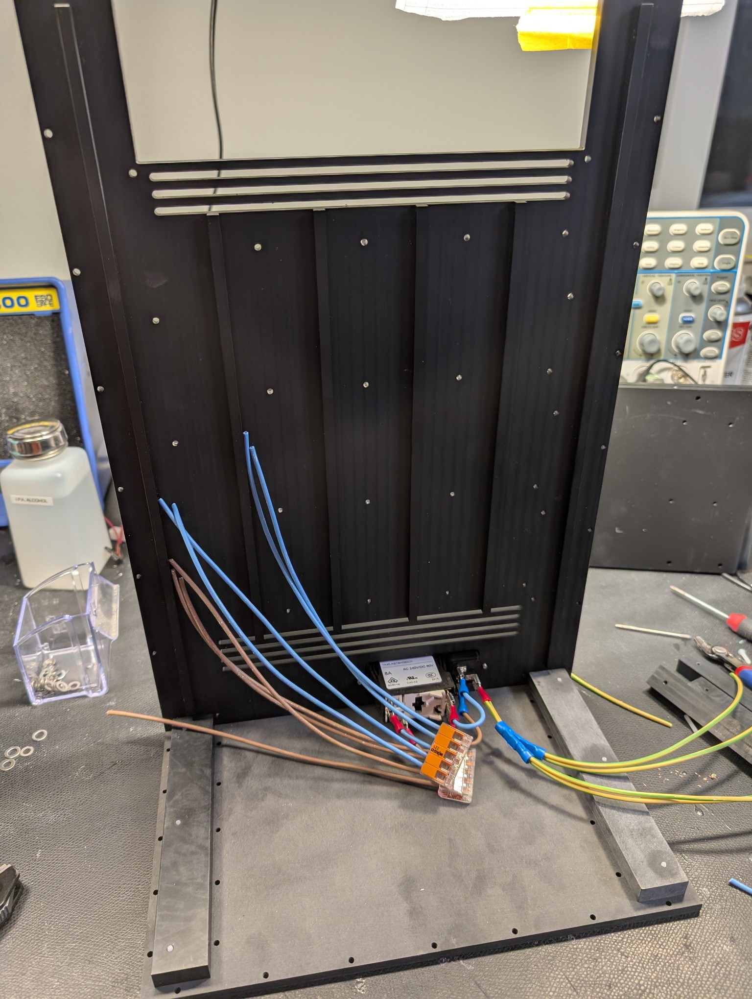
  • Final assembly #1 - heat sink

    Simon Trendel • 11/06/2025 at 12:16 • 0 comments

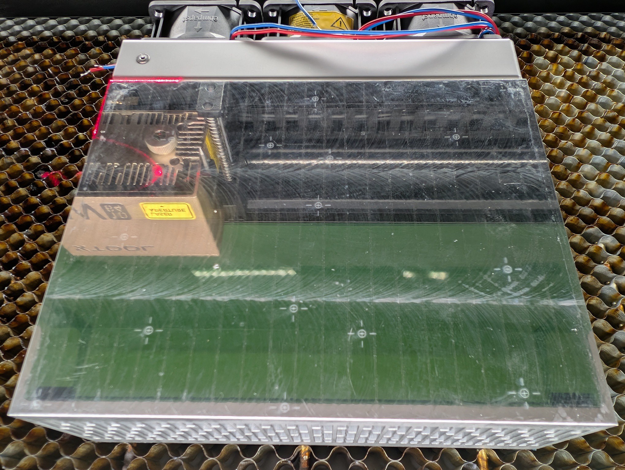
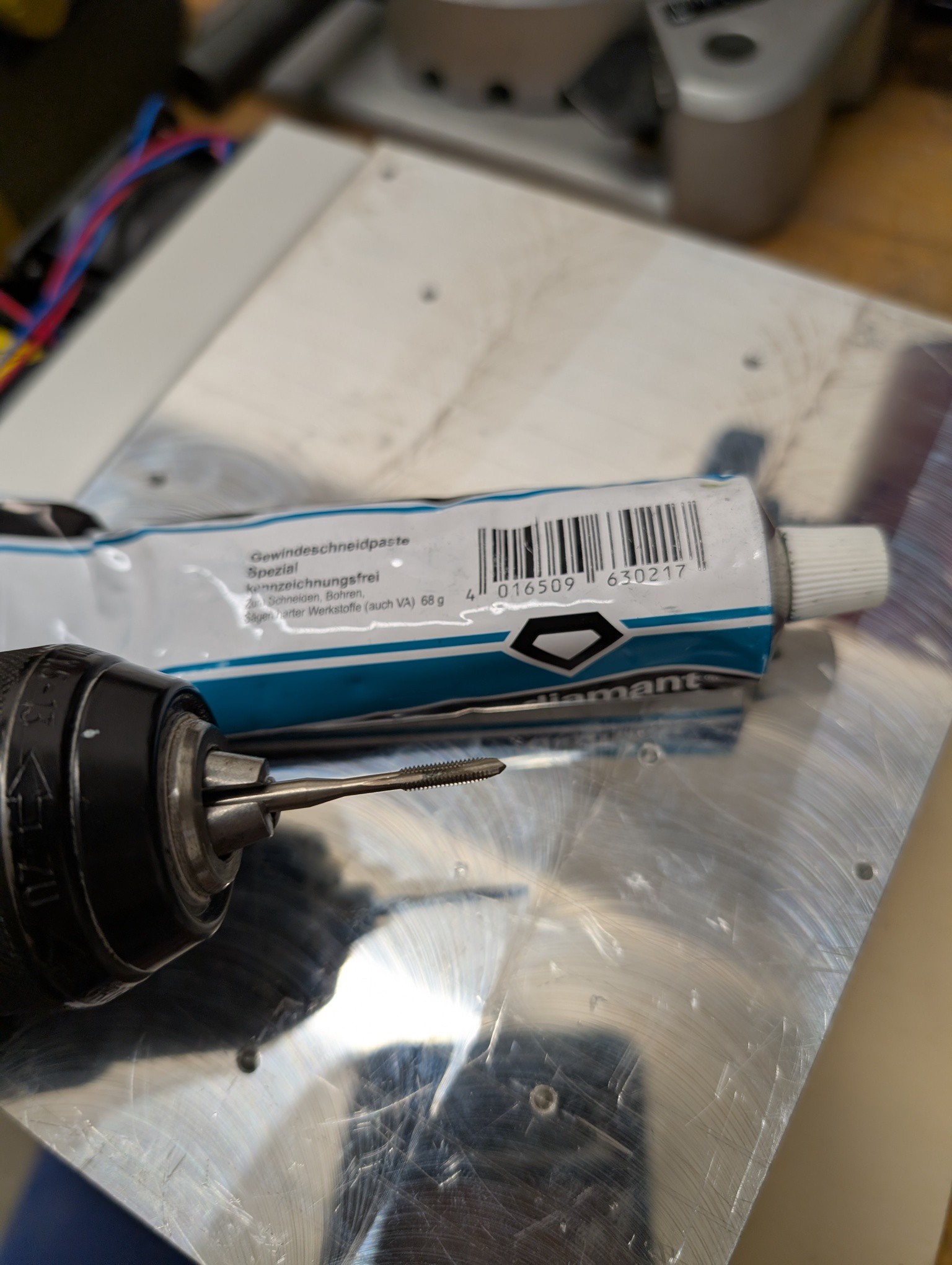
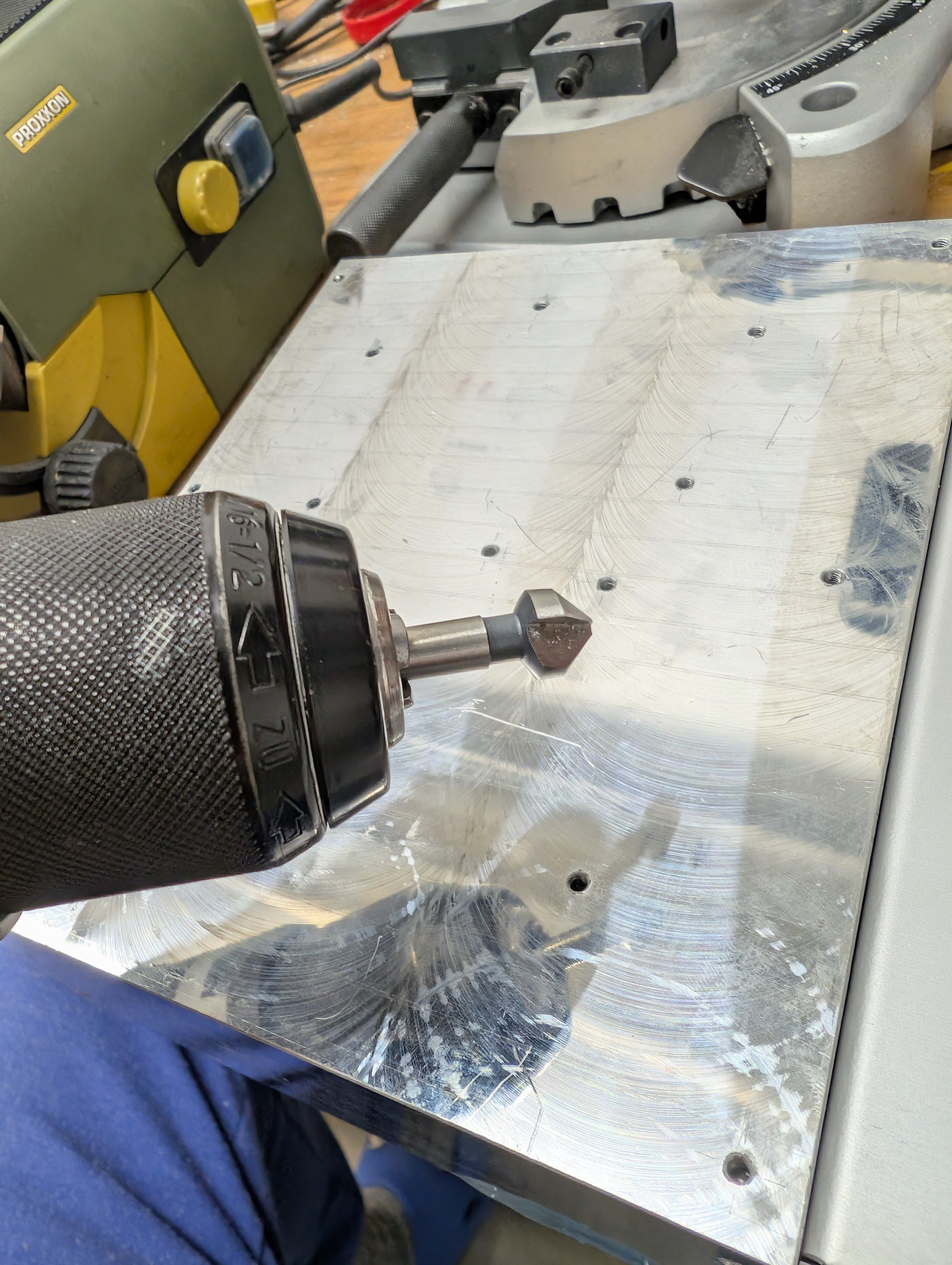
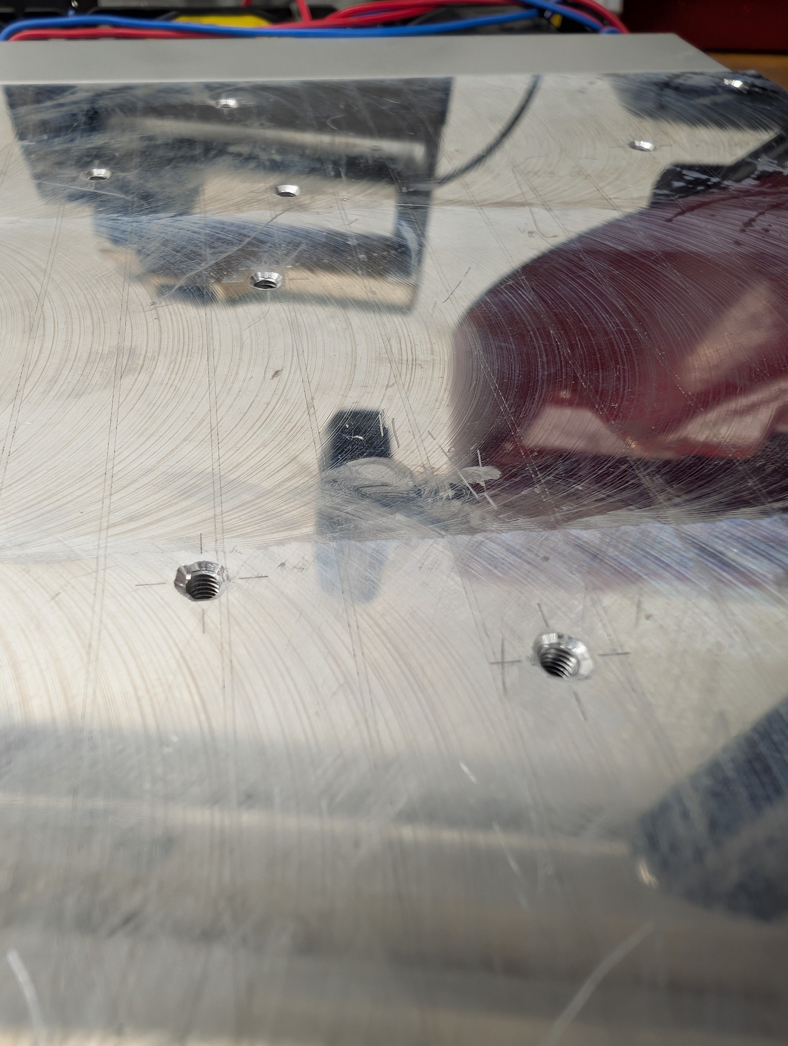
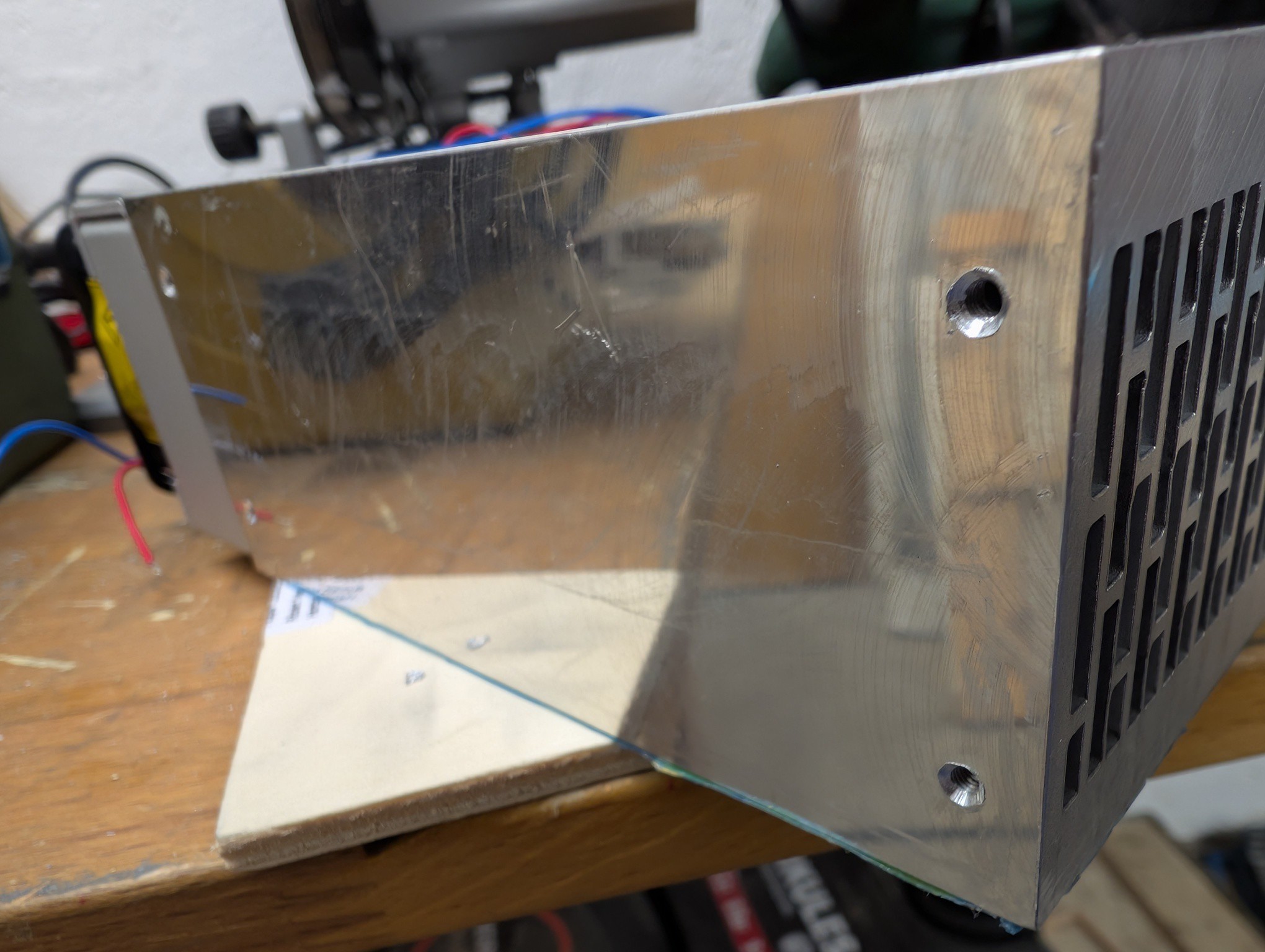
    Heat sink holes and threading:

  • Testing the electronics

    Simon Trendel • 11/06/2025 at 12:01 • 0 comments

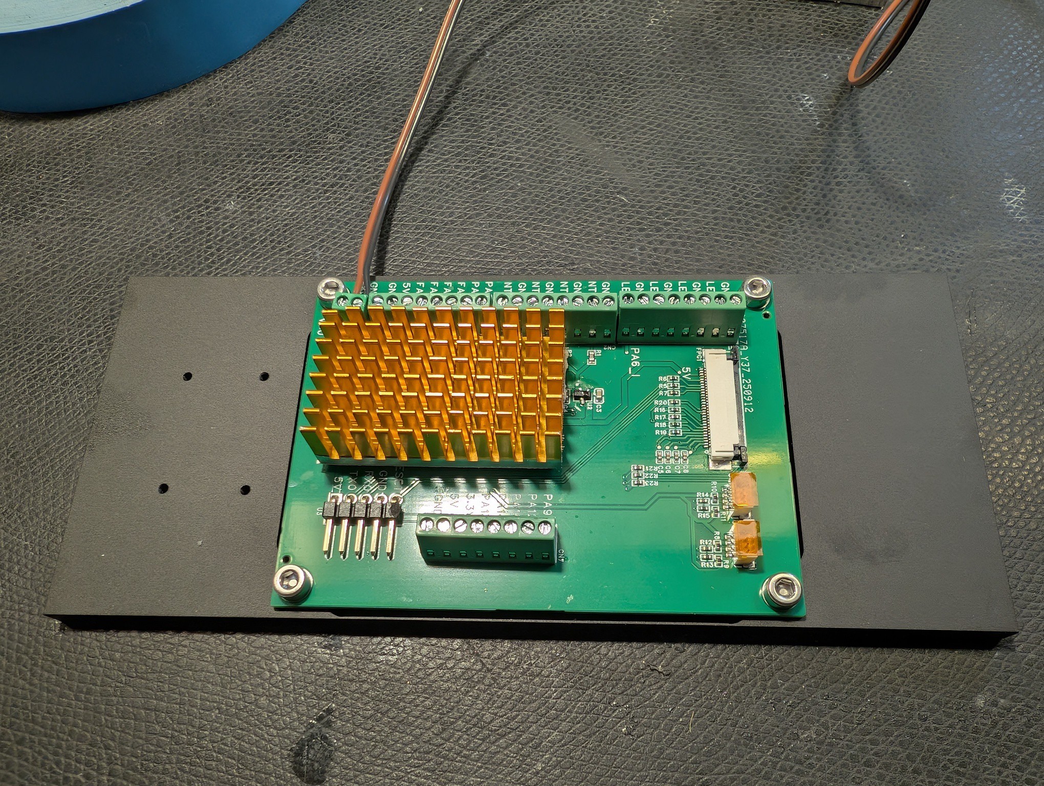
    All parts arrived and it was time to test.

    All boards had mistakes :( . But all could be fixed on the PCBs. 

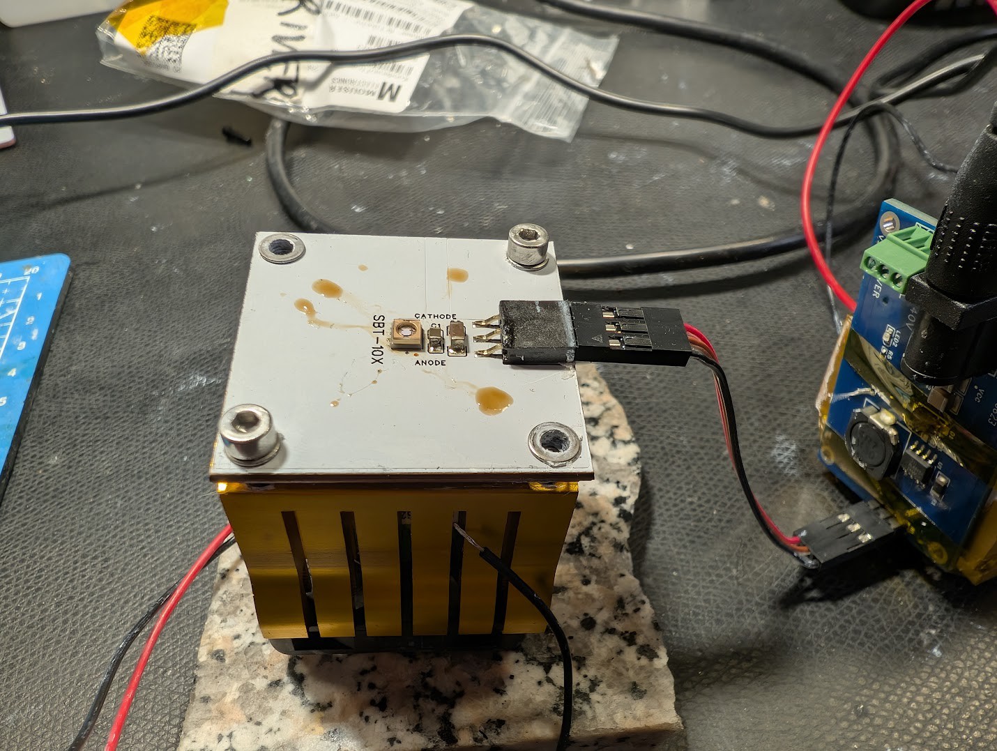
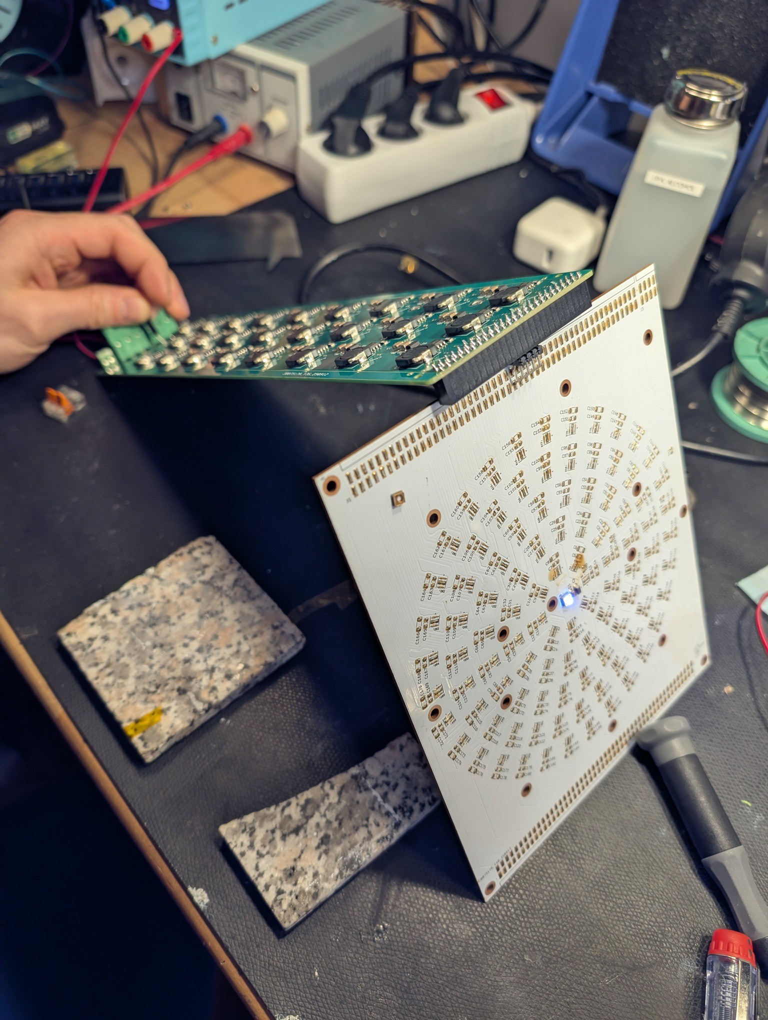
    After the initial light test, I assembled one SBT-10X LED to the copper core PCB. It turned out, I had wired the driver edge connector incorrectly. Luckily the LED footprint is symmetric, so I could simply assemble the LED 180 deg rotated. I burned only two LEDs until I realized the mistake.

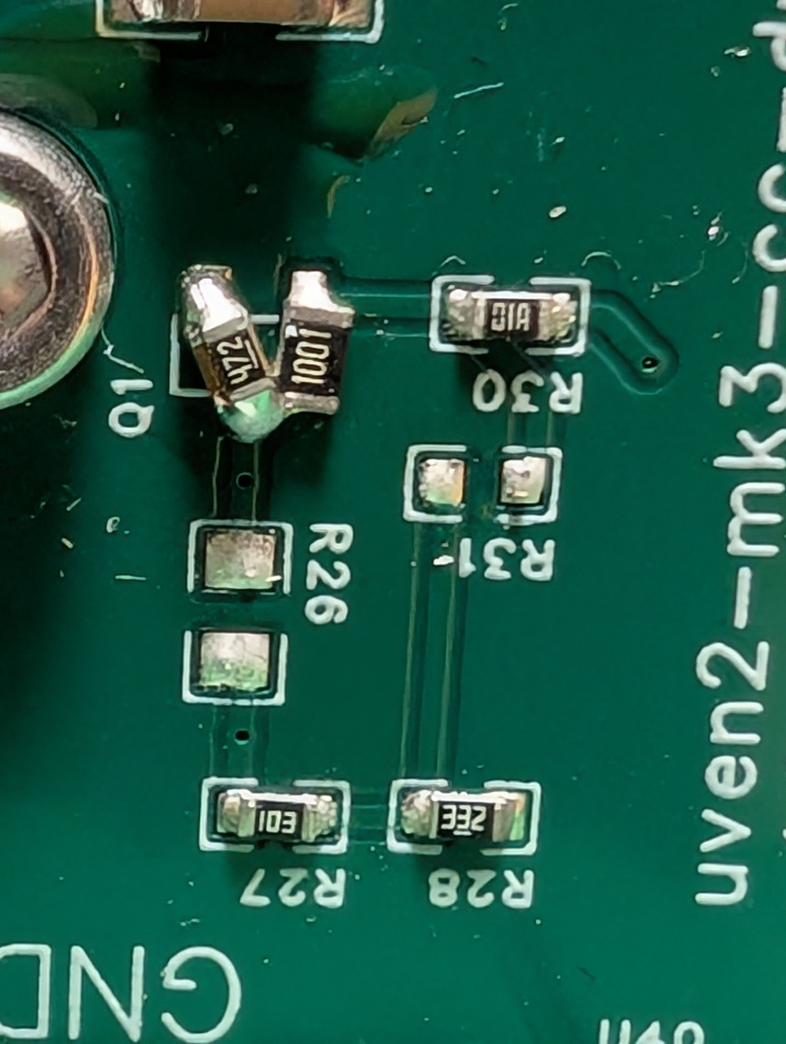
    The driver PCB had another mistake that was more subtle and took a while to figure out. The mistake was to drive the CTRL pin of the led driver IC using 12V. That pin has a max voltage of 3.3V and driving it with higher voltage can damage the IC. So I removed the mosfet and pulled the CTRL pin low. 

    There are two mistakes on the main-board. They are both very dumb, but luckily could be fixed on the main board PCB. 

    The first mistake was to wire the EPAD pin of the 12V->5V and 12->3.3V DCDC converters to GND. For the fixed voltage version I assembled, this pin needs to be floating and serves as thermal heat sink. I simply cut the pins and added an external heat sink. 

    The second mistake was not having checked the datasheet of the heat sink fans. Turns out they draw 4A@12V, which immediately annihilated the MOSFET I had planned for them. 

    All mistakes are fixed in the latest version on github.

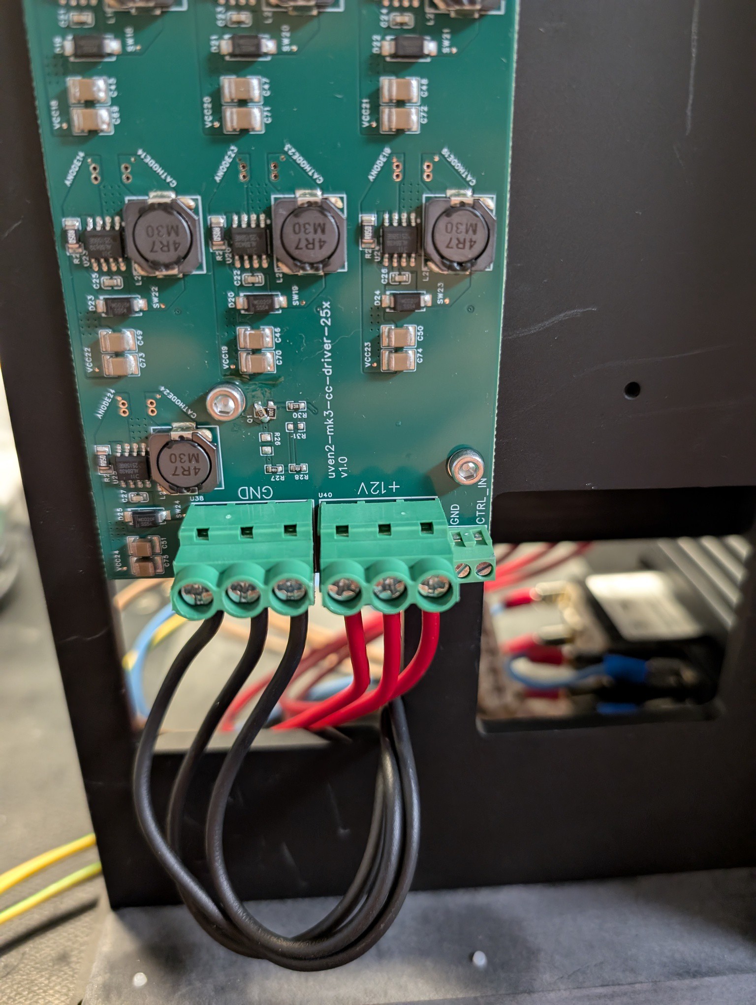
    I fixed all drivers and tested all channels of each driver.

    Next I assembled the full LED panel (with the LEDs rotated 180deg)

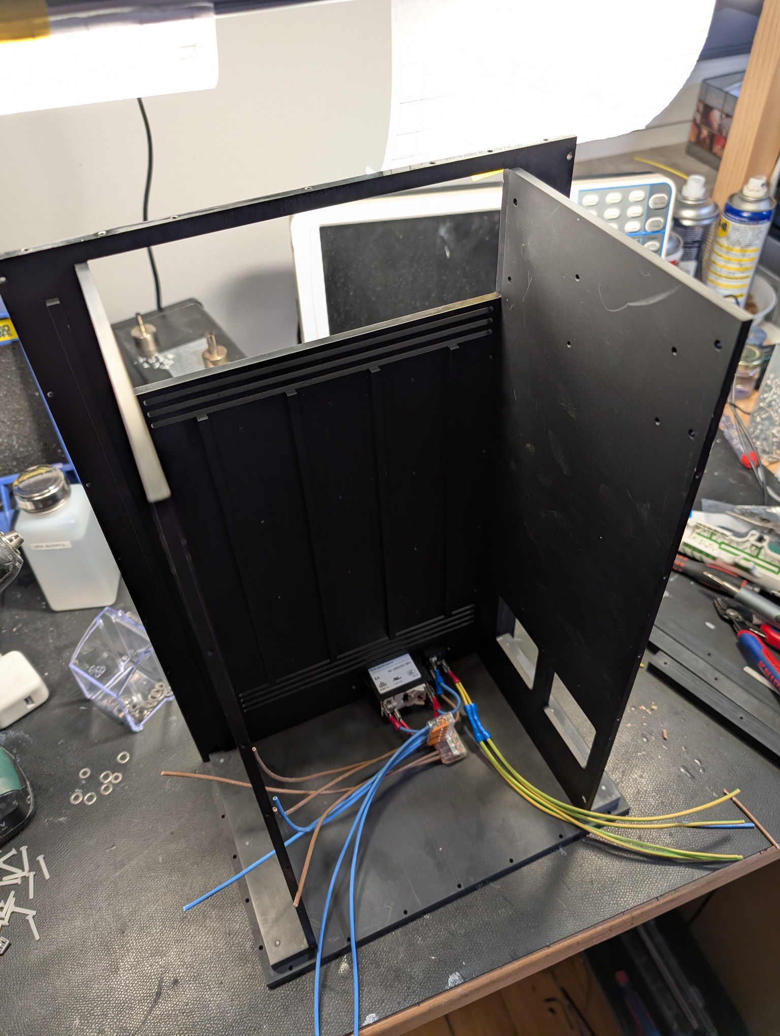
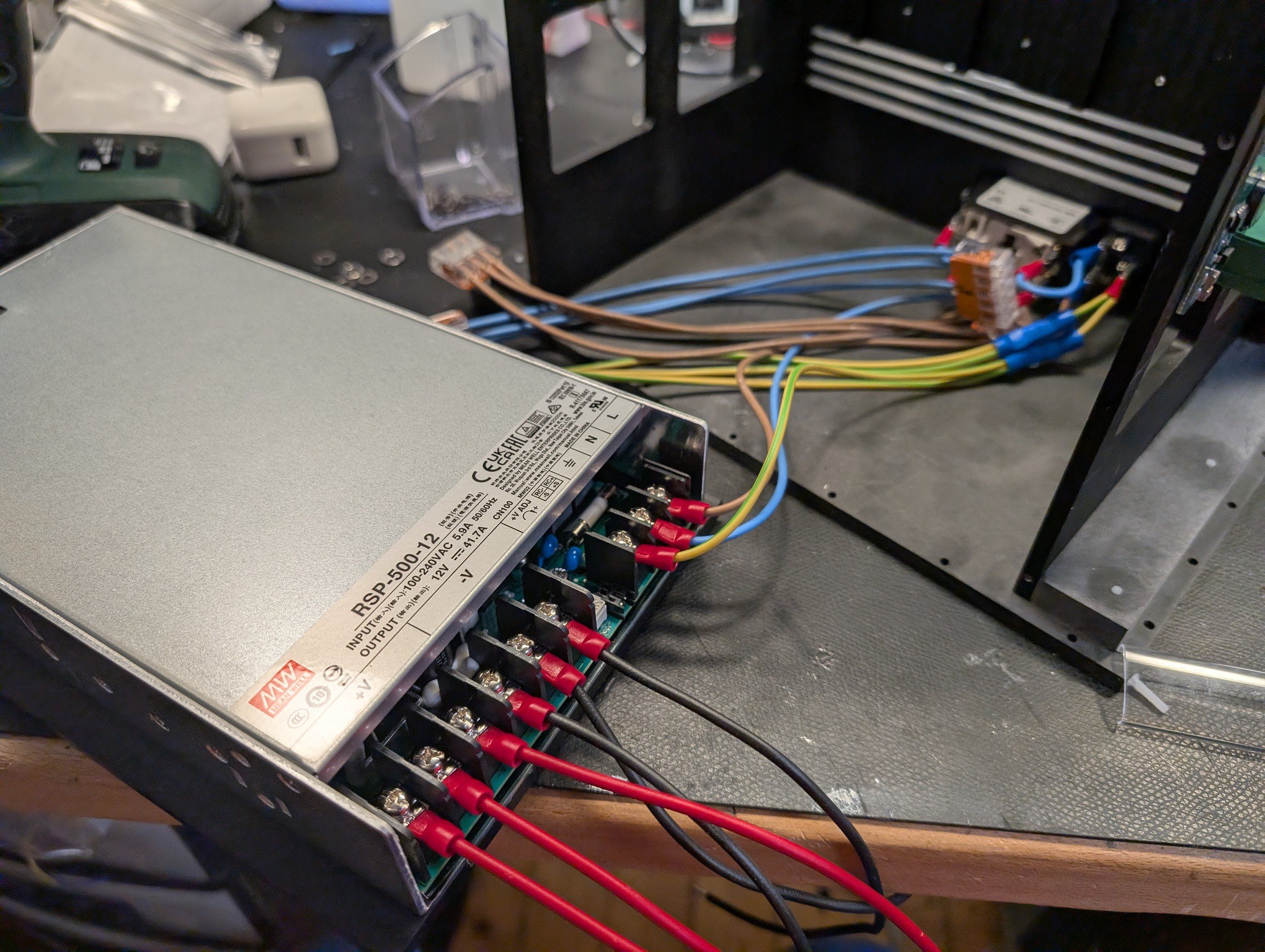
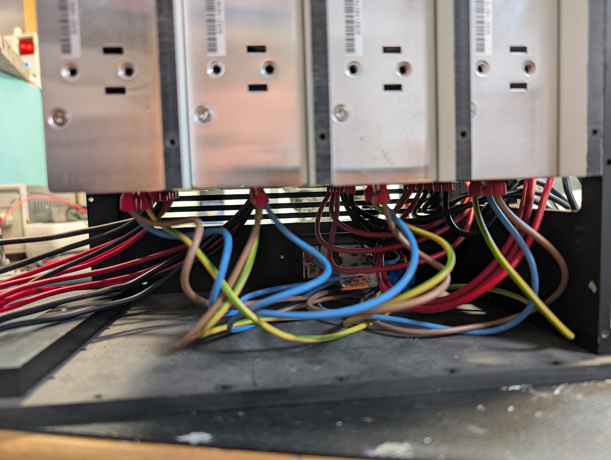
    For testing the full panel I needed to assemble the rest of the lamp.

  • Final mechanical design

    Simon Trendel • 09/03/2025 at 11:00 • 0 comments

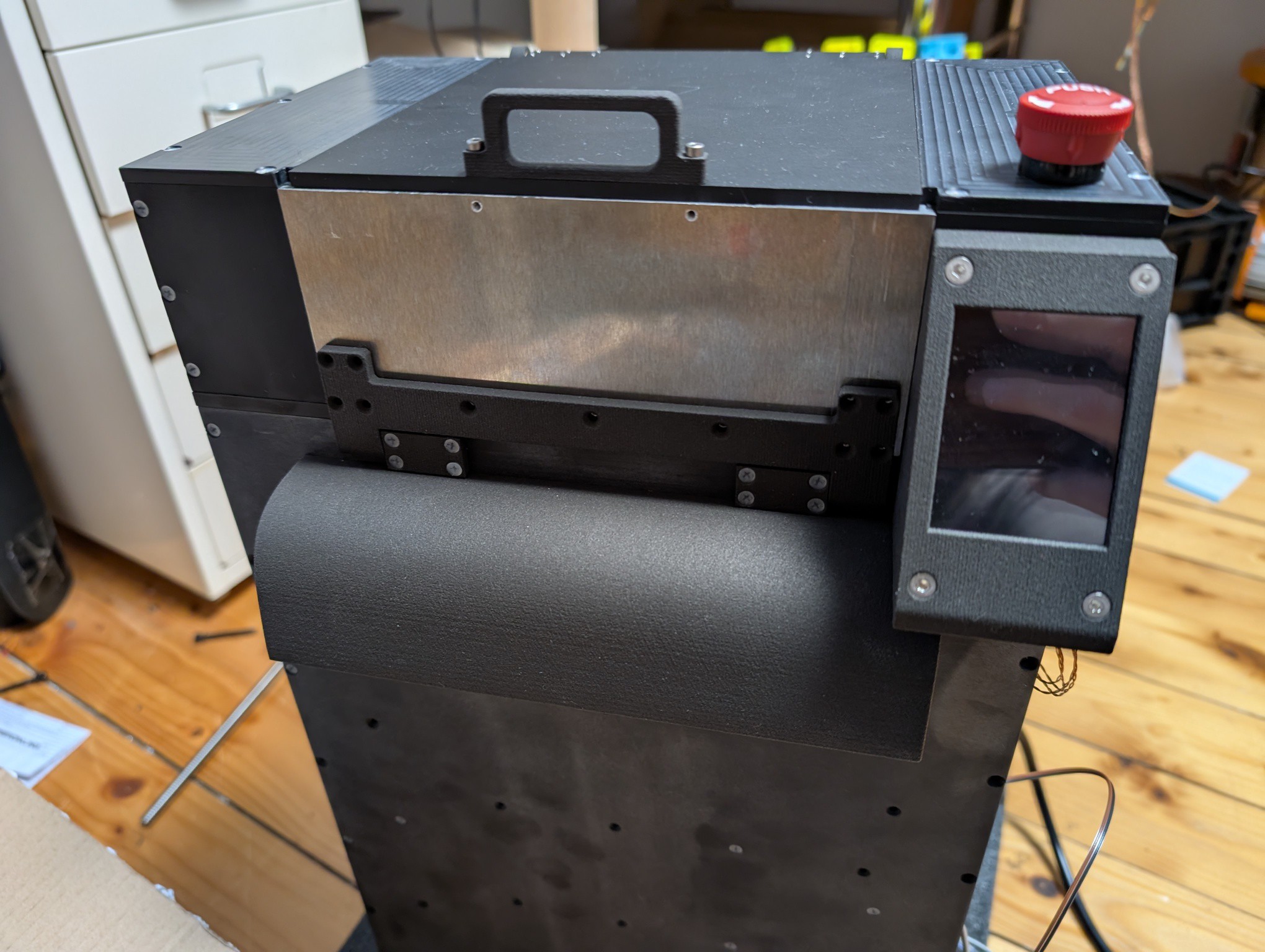
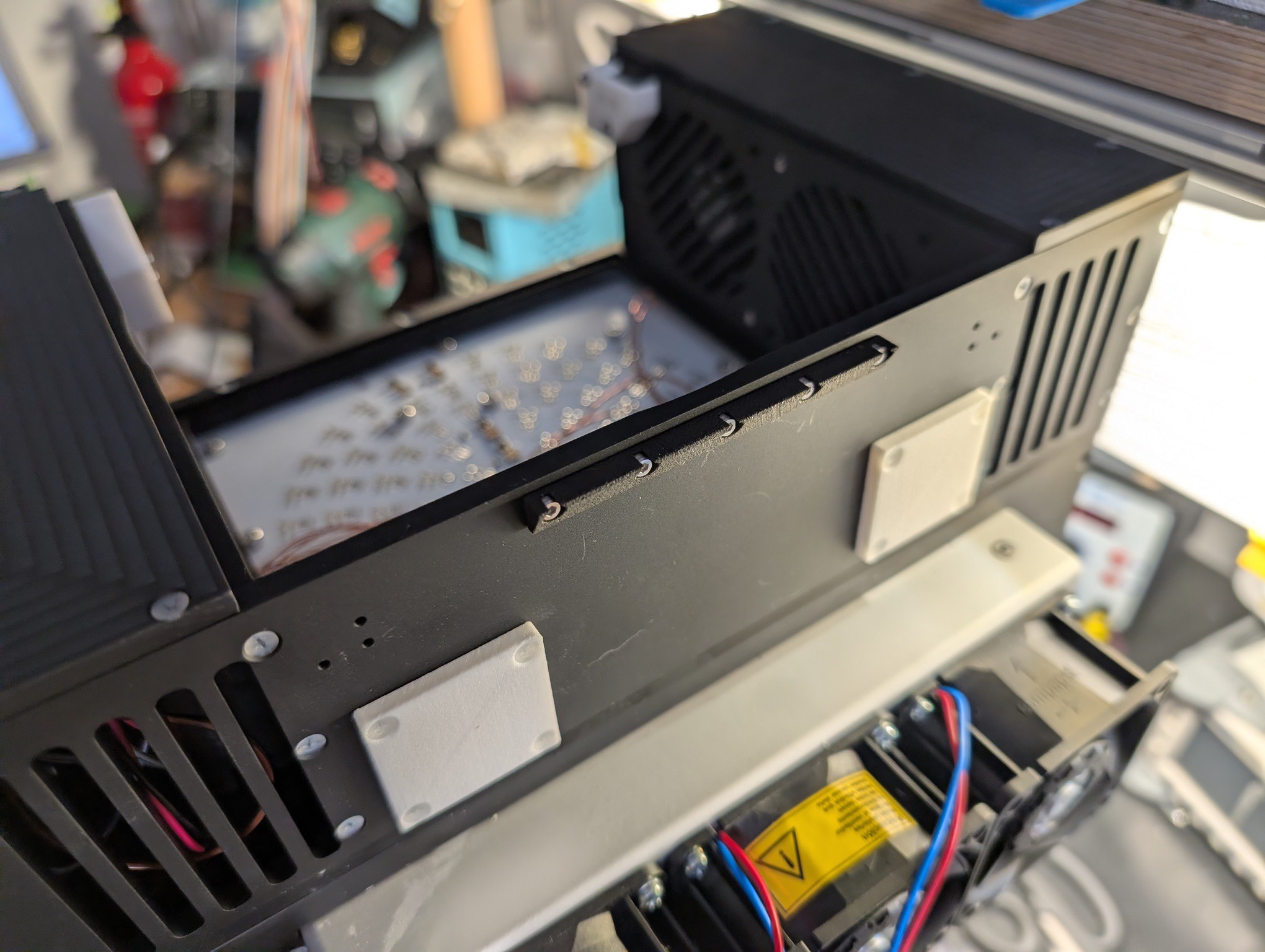
    We decided it was a good idea to make the chamber front loadable as well. With all the final mechanical details the lamp is ready for order:

  • mechanical design

    Simon Trendel • 07/12/2025 at 17:35 • 0 comments

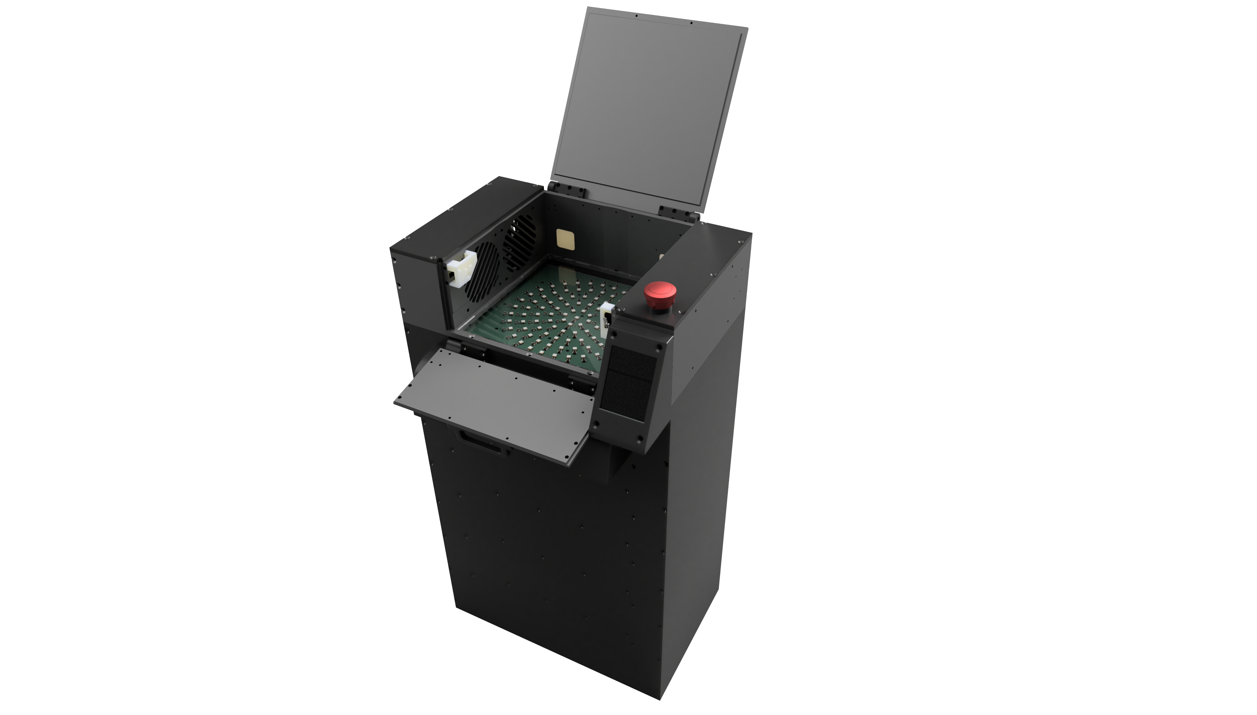
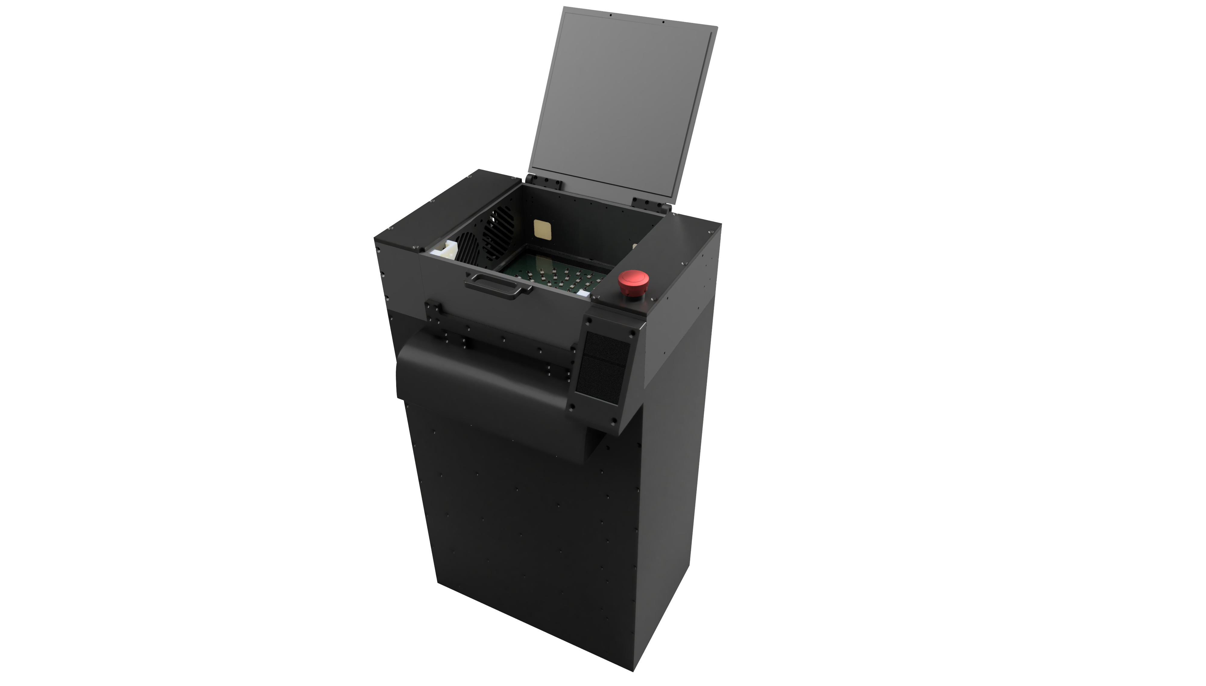
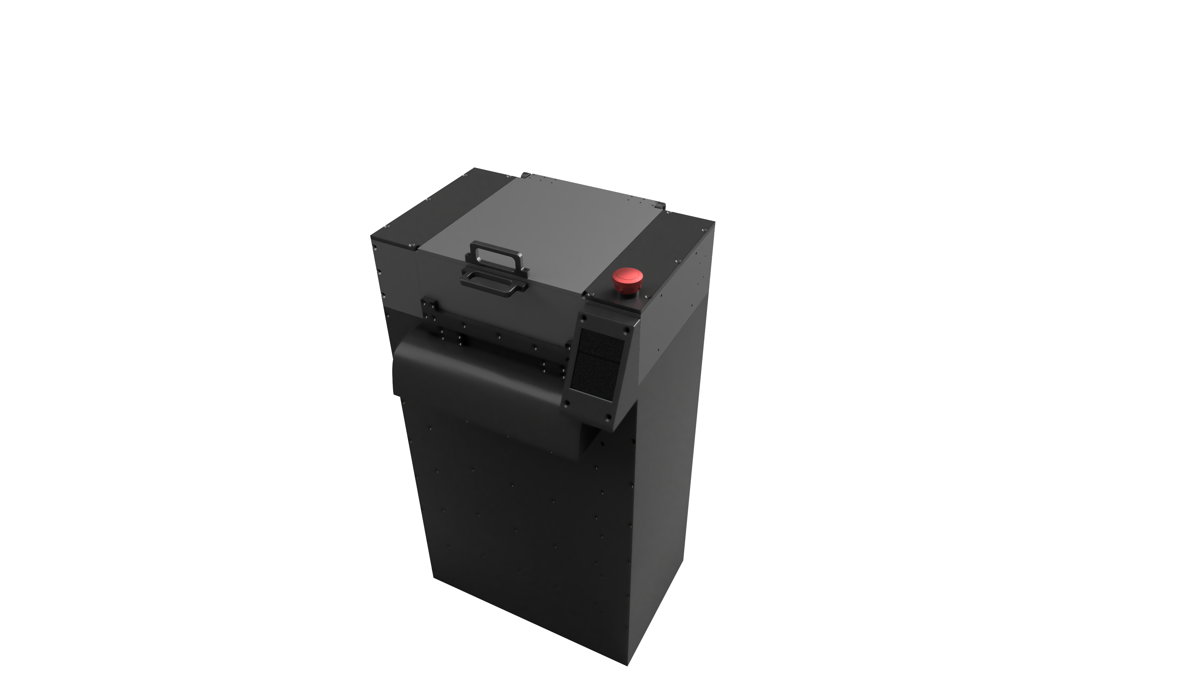
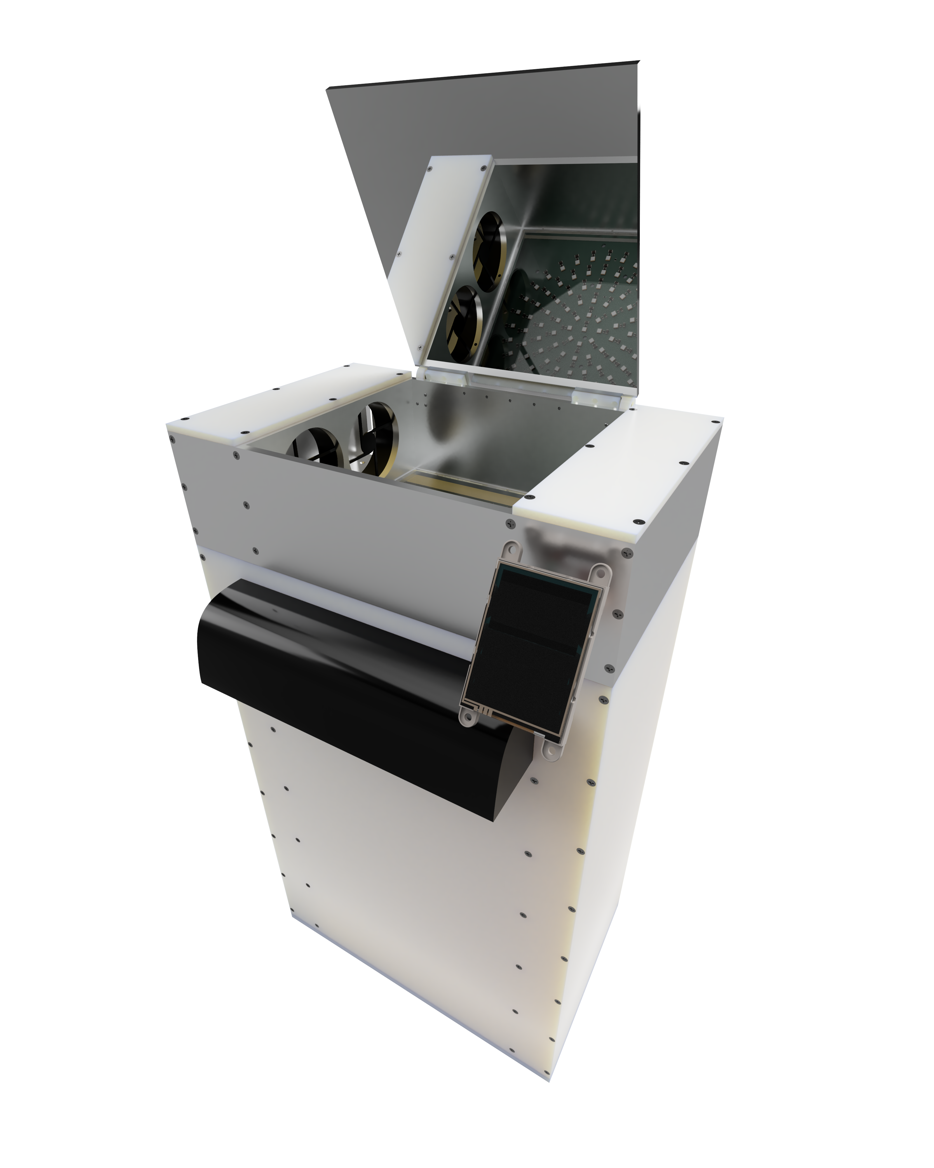
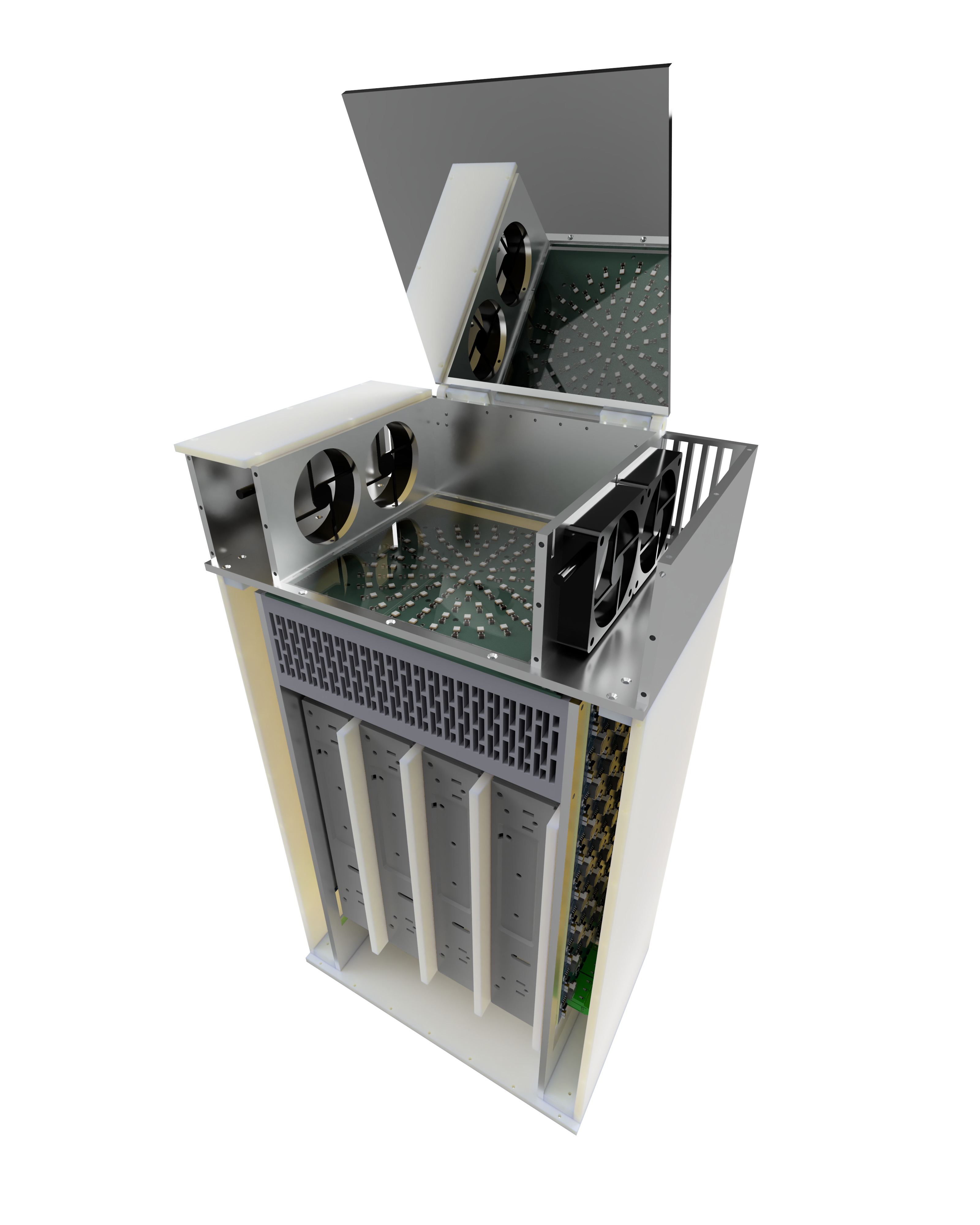
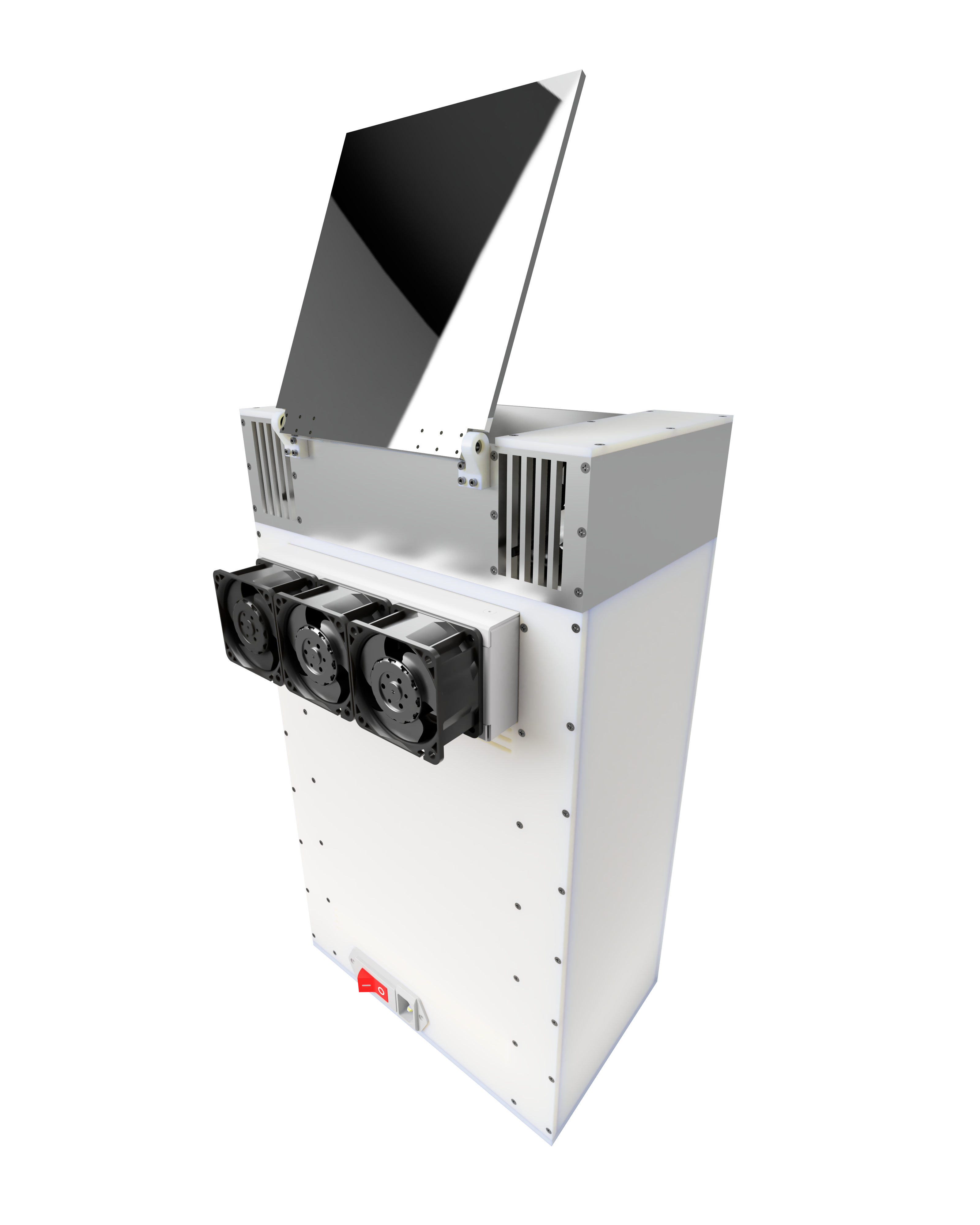
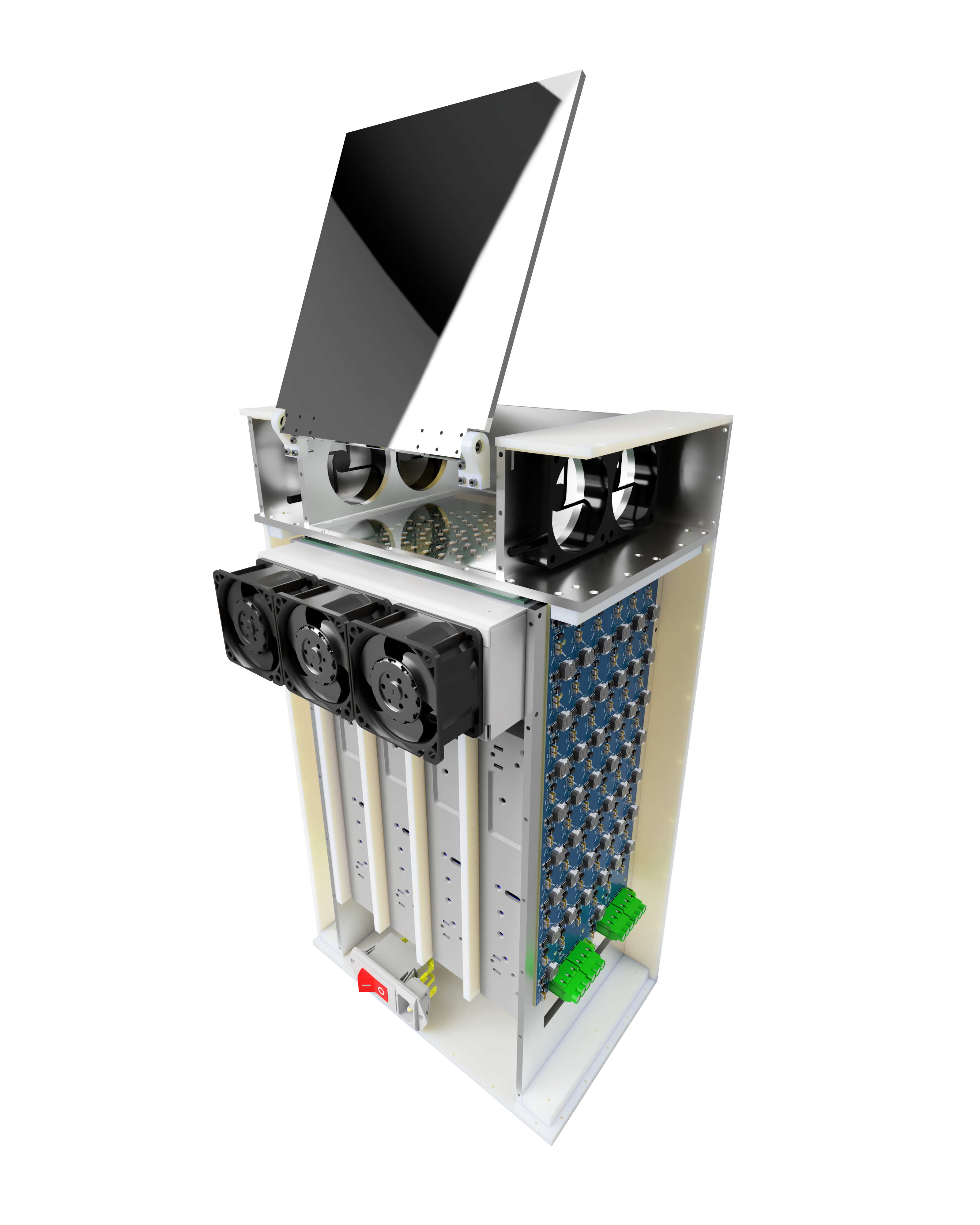
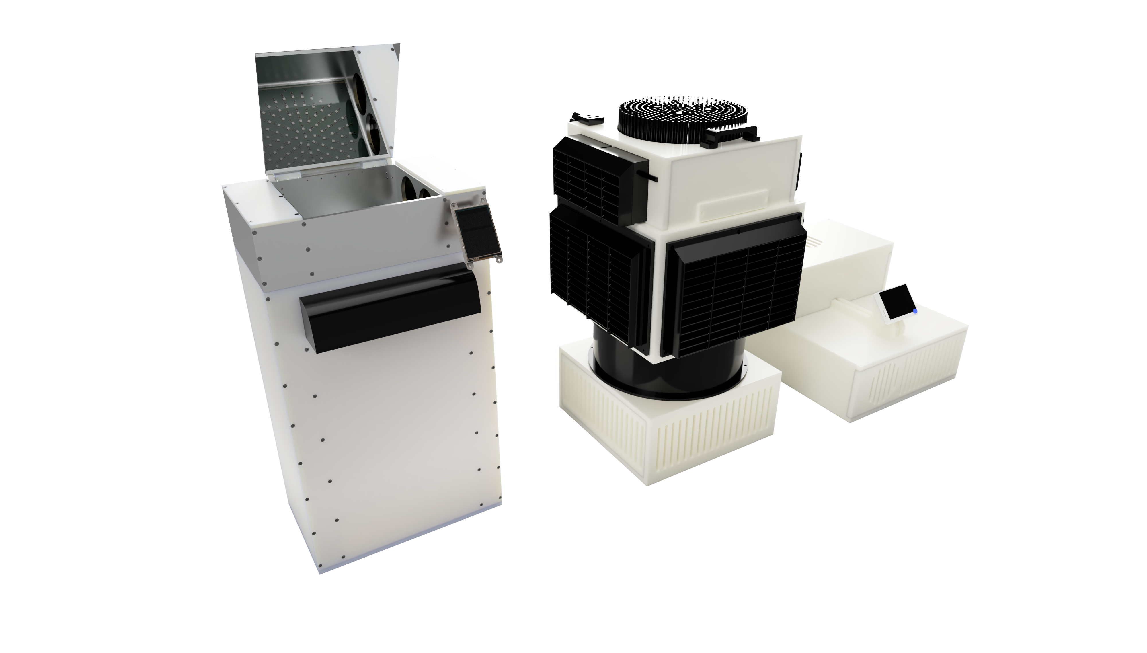
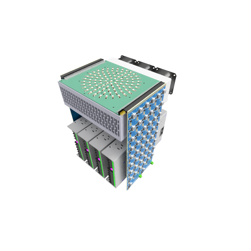
    With the main PCBs ready it was time to finalize the mechanical design. The following pictures show renderings of the front and the back of the lamp:

    And here is a size comparison with the previous version mk2:

  • 25x cc driver

    Simon Trendel • 07/06/2025 at 18:46 • 0 comments

    For the 25x driver PCB I decided to control all drivers simultaneously using the CTRL pin of the AL8843. By default all drivers should be off, even if no MCU is actively controlling the board.

    To achieve this I'm using an N-MOSFET that is default conducting, pulling all CTRL pins low. If the MCU is connected, it can drive the CTRL_IN pin accordingly. Because the MCU will run at 3.3V, I use a voltage divider to set the gate voltage to 3.3V default.

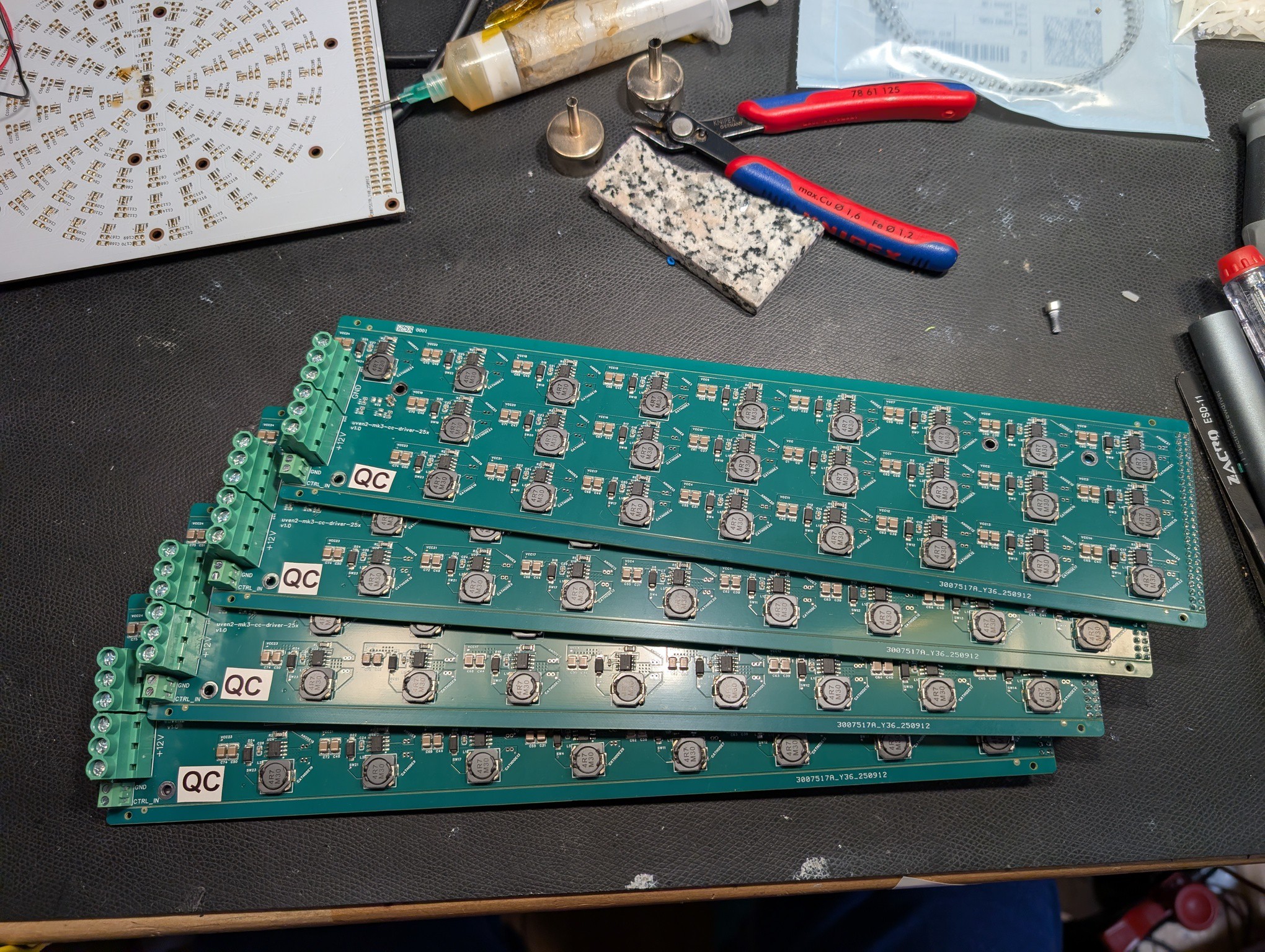
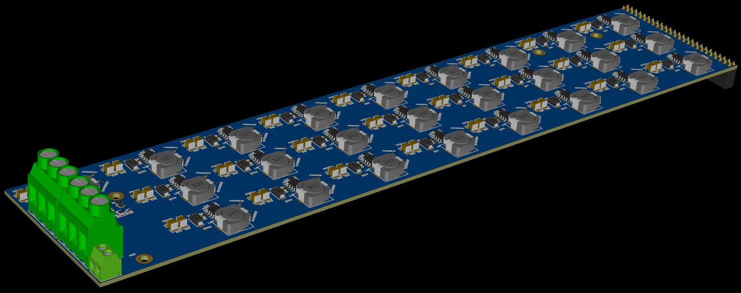
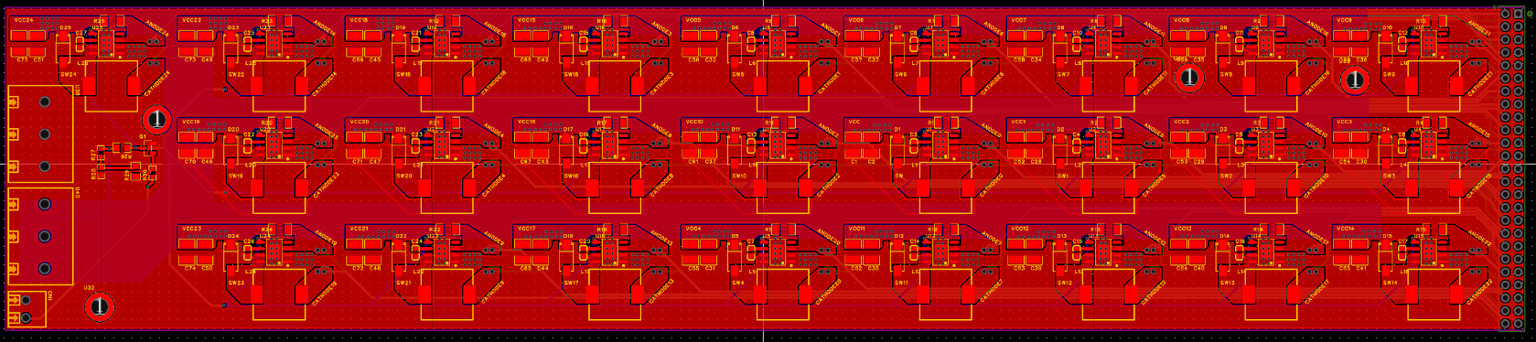
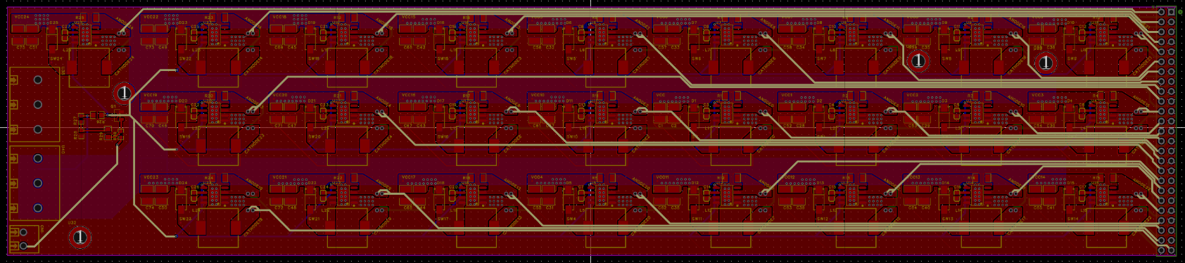
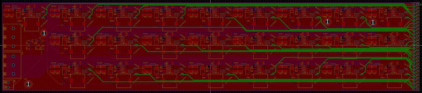
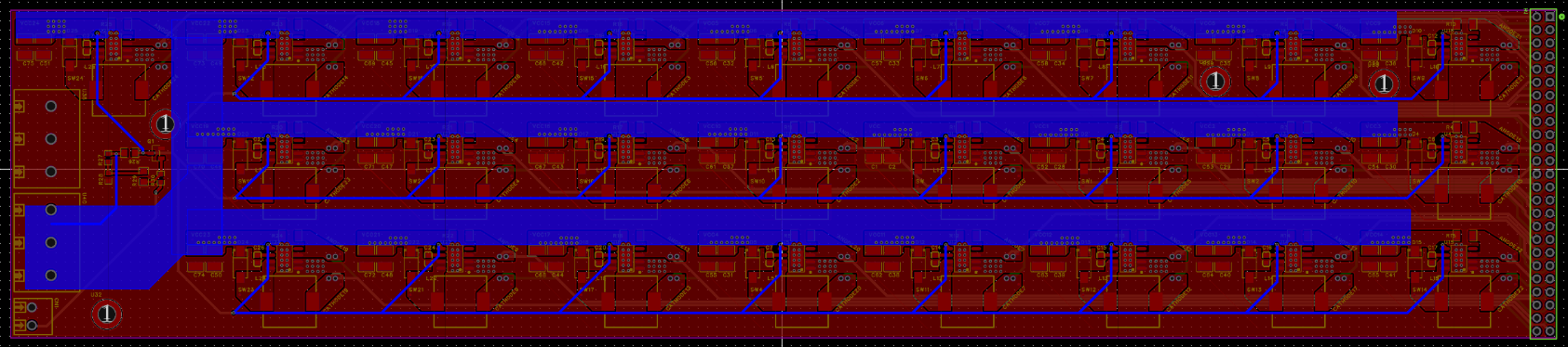
    The finished driver looks like this:

    Top: 

    Inner1:

    Inner2:

    Bottom:

    The default track width is 0.5mm. With 2oz copper for inner and outer copper layers, this should be enough for conducting the LED currents safely.

    For each LED panel with 100 LEDs we plug 2 of these 25x driver boards on either side of the panel. The full lamp is starting to take form:

  • 100x LED panel

    Simon Trendel • 07/05/2025 at 14:23 • 0 comments

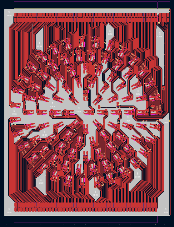
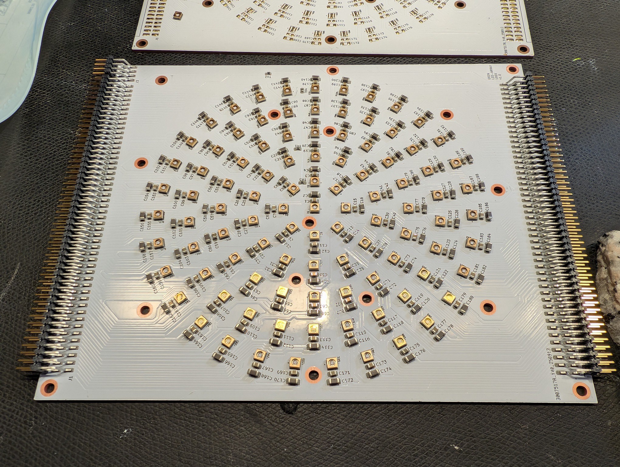
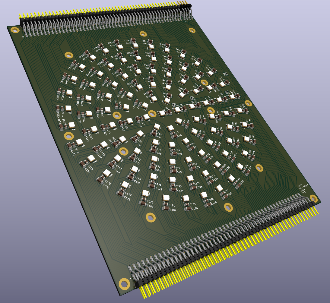
    Next I designed the LED panel. We chose 100x LEDs for this version. The spacing is as uniform as possible. Unfortunately EasyEDA doesn't seem to have any way of positioning components in a programmatic way, so for this PCB I'm using KiCAD again. KiCAD has a python scripting console and I used the following script to place all the components automatically.

    import math
    import pcbnew
    
    board = pcbnew.GetBoard()
    
    # Ring configuration
    rings = {
        0: 1,
        1: 8,
        2: 14,
        3: 20,
        4: 26,
        5: 31
    }
    
    ring_spacing_mm = 12
    cap_spacing_mm_1 = 3.5
    cap_spacing_mm_2 = 2.6
    center_x_mm = 100
    center_y_mm = 111
    ref_offset_mm = 1.5  # tangential offset
    
    def mm_to_nm(val):
        return int(val * 1_000_000)
    
    center = pcbnew.VECTOR2I(mm_to_nm(center_x_mm), mm_to_nm(center_y_mm))
    ref_counter = 1
    
    for ring_index, led_count in rings.items():
        radius_mm = ring_index * ring_spacing_mm
    
        for i in range(led_count):
            angle_rad = -2 * math.pi * i / led_count
            angle_deg = -math.degrees(angle_rad)
    
            dx = math.cos(angle_rad)
            dy = math.sin(angle_rad)
            tangent_dx = -dy
            tangent_dy = dx
    
            # LED
            led_ref = f"D{ref_counter}"
            r_led = radius_mm
            led_pos = pcbnew.VECTOR2I(
                center.x + mm_to_nm(r_led * dx),
                center.y + mm_to_nm(r_led * dy)
            )
            led_fp = board.FindFootprintByReference(led_ref)
            if led_fp:
                led_fp.SetPosition(led_pos)
                led_fp.SetOrientationDegrees(angle_deg - 90)
                c1_txt = c1_fp.Reference()
                c1_txt.SetVisible(True)
                c1_txt.SetTextAngleDegrees(0)
                c1_txt.SetPosition(pcbnew.VECTOR2I(
                    c1_pos.x + mm_to_nm(0),
                    c1_pos.y + mm_to_nm(0)
                ))
    
            # Capacitor 1
            c1_ref = f"C{2 * (ref_counter - 1) + 1}"
            r_c1 = r_led + cap_spacing_mm_1
            c1_pos = pcbnew.VECTOR2I(
                center.x + mm_to_nm(r_c1 * dx),
                center.y + mm_to_nm(r_c1 * dy)
            )
            c1_fp = board.FindFootprintByReference(c1_ref)
            if c1_fp:
                c1_fp.SetPosition(c1_pos)
                c1_fp.SetOrientationDegrees(angle_deg + 90)
                c1_txt = c1_fp.Reference()
                c1_txt.SetVisible(True)
                c1_txt.SetTextAngleDegrees(0)
                c1_txt.SetPosition(pcbnew.VECTOR2I(
                    c1_pos.x + mm_to_nm(0),
                    c1_pos.y + mm_to_nm(0)
                ))
    
            # Capacitor 2
            c2_ref = f"C{2 * (ref_counter - 1) + 2}"
            r_c2 = r_c1 + cap_spacing_mm_2
            c2_pos = pcbnew.VECTOR2I(
                center.x + mm_to_nm(r_c2 * dx),
                center.y + mm_to_nm(r_c2 * dy)
            )
            c2_fp = board.FindFootprintByReference(c2_ref)
            if c2_fp:
                c2_fp.SetPosition(c2_pos)
                c2_fp.SetOrientationDegrees(angle_deg + 90)
                c2_txt = c2_fp.Reference()
                c2_txt.SetVisible(True)
                c2_txt.SetTextAngleDegrees(0)
                c2_txt.SetPosition(pcbnew.VECTOR2I(
                    c2_pos.x + mm_to_nm(0),
                    c2_pos.y + mm_to_nm(0)
                ))
    
            ref_counter += 1
    
    pcbnew.Refresh()
    board.Save(board.GetFileName())
    print("✅ Components and reference labels updated with tangential offsets.")

    Routing was a bit tricky, because for a copper base board you can only route on the top of the board. I included 4 NTC thermistors as well, so we can get feedback on the LED temperature.

    The LED driver boards will be connected on either side of the LED panel using the 2.54mm pin headers.

View all 11 project logs

View all instructions

Enjoy this project?

Share

Discussions

Similar Projects

Does this project spark your interest?

Become a member to follow this project and never miss any updates