kooksay
-
Status Update Recently
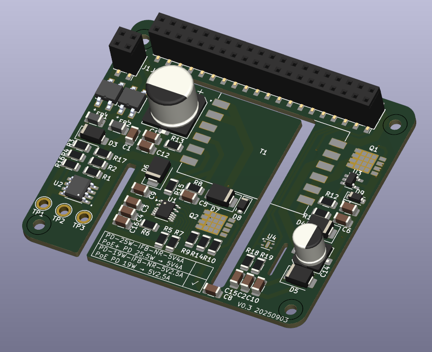
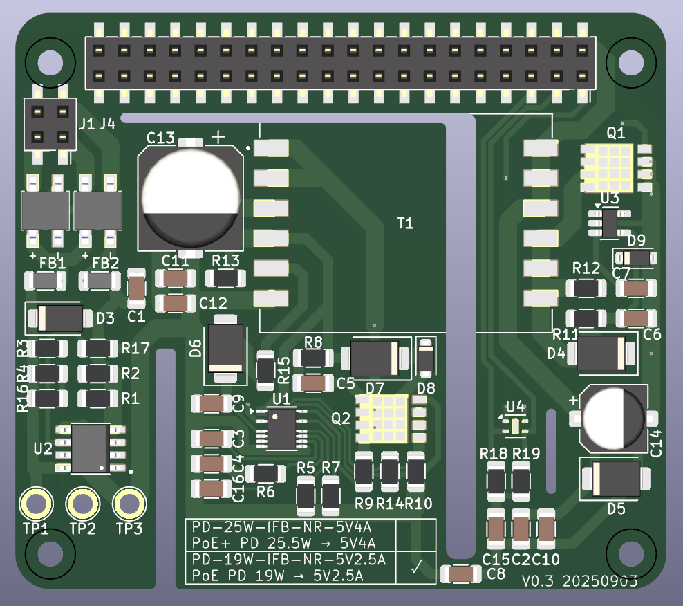
09/05/2025 at 16:41 • 0 commentsRecently, I haven’t had time to continue improving the 1x2 audio switcher because I’ve been helping a friend design a PoE-HAT circuit board. Fortunately, I finally completed the initial design of this new board today, and after it’s delivered next week, I’ll be able to get back to working on the audio switcher.
-
The Assembled Look Of The Switcher With Enclosure
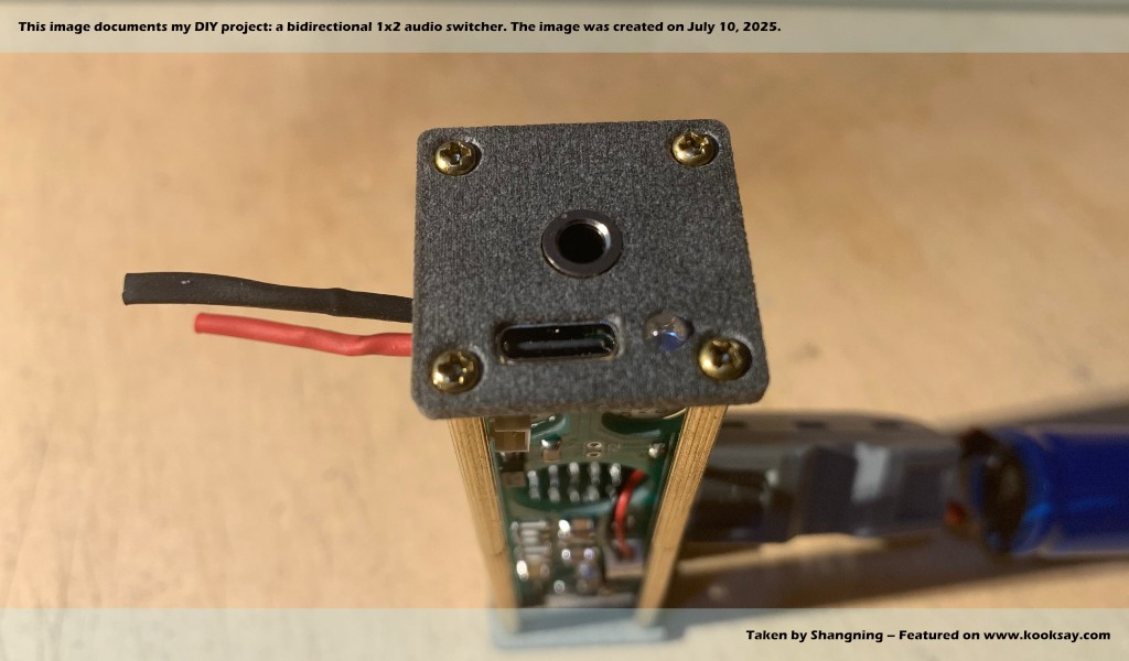
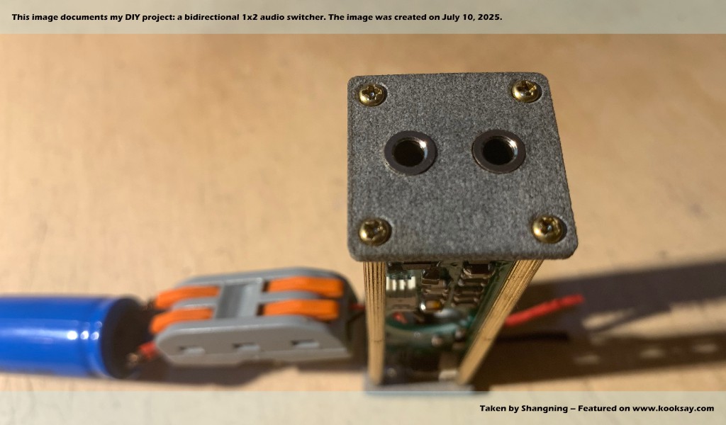
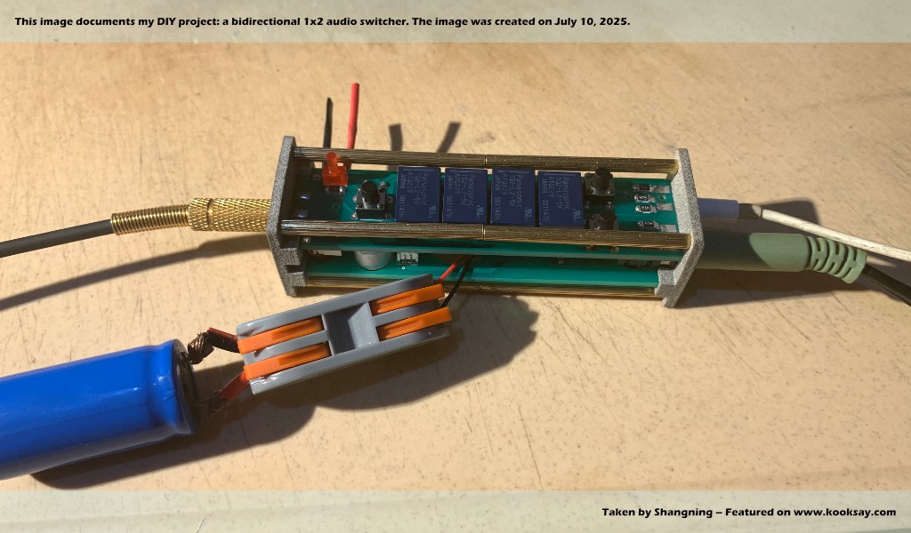
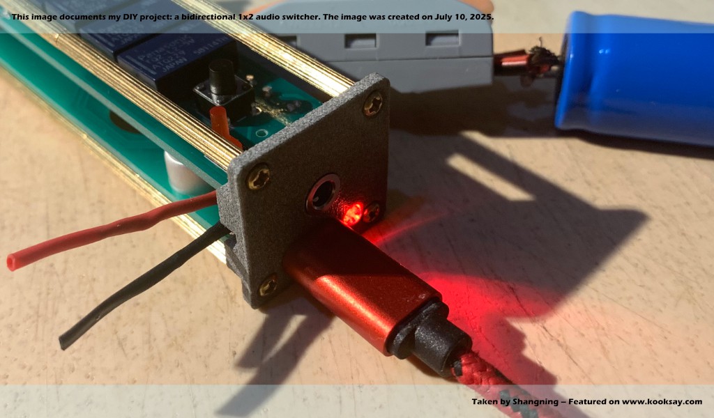
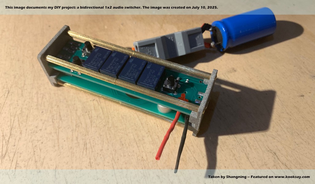
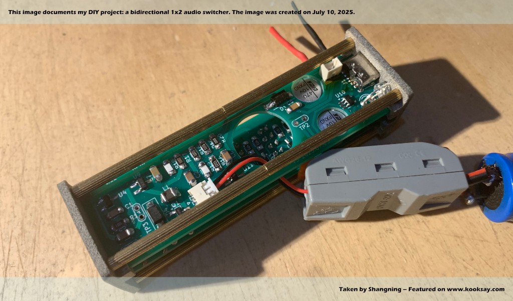
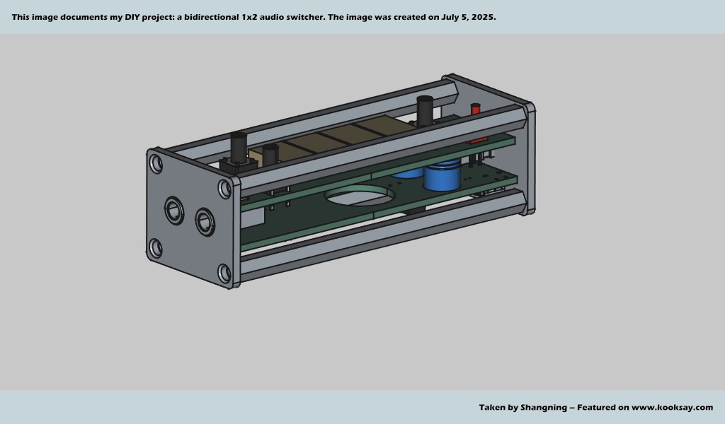
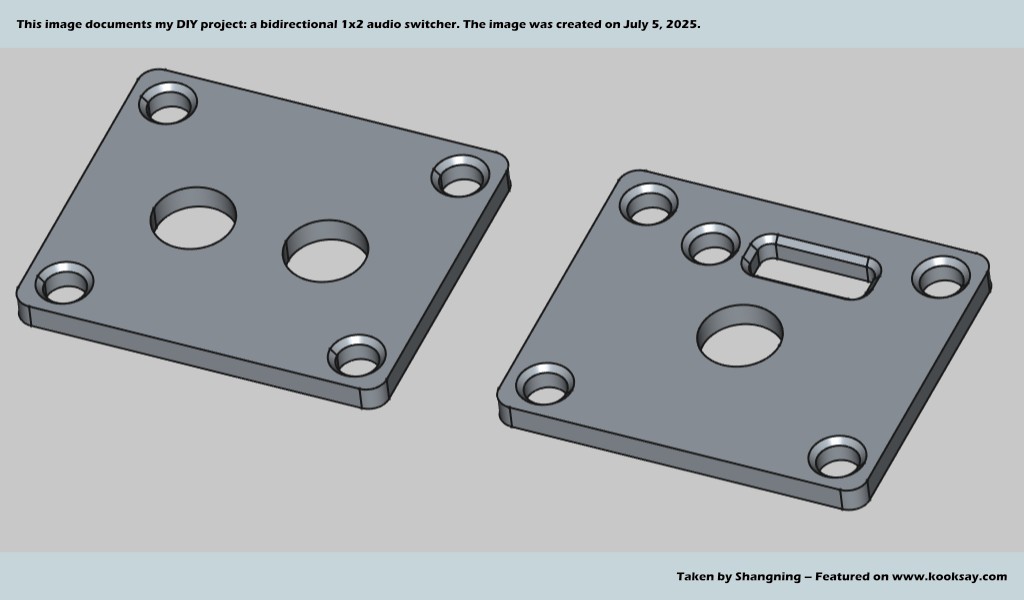
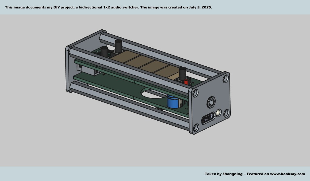
07/10/2025 at 16:32 • 0 commentsToday, I completed the initial design of the enclosure for the 1×2 audio switcher. Although this “enclosure” isn’t yet a true casing in the strict sense, it currently consists of a frame structure built with four standoffs. Still, in my view, this form is already quite close to the final product.
![]()
![]()
![]()
![]()
![]()
![]()
-
It's time to design the enclosure and the panel.
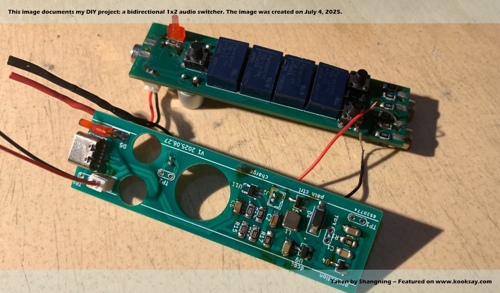
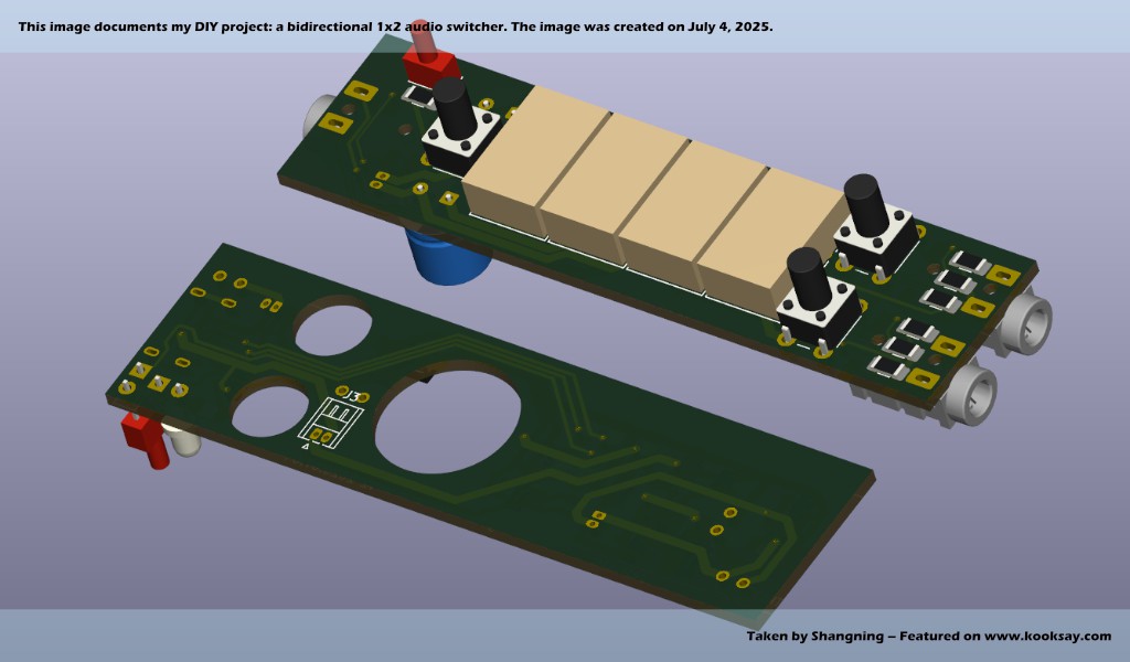
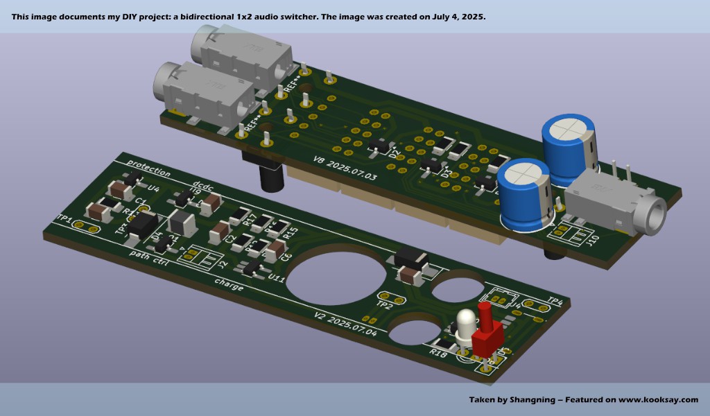
07/04/2025 at 16:07 • 0 commentsThe circuit boards for both parts of the circuit have been basically completed. It's time to design the enclosure and the panel.
![]()
![]()
![]()
-
The Basic Functionality Is Working Properly
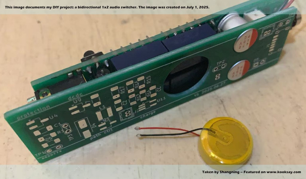
07/03/2025 at 18:30 • 0 commentsThe power board has been received, soldered, and tested successfully. The signal board has also been connected, and the overall circuit is functioning properly as expected.
![]()
However, I feel there are still some details that need refinement, so I made some minor adjustments to the circuit today and am preparing to send it to the factory again. In fact, this round of adjustments doesn't involve significant changes to the circuit's functionality; it mainly focuses on fine-tuning the layout of the ICs to make it more suitable for manual soldering.
![]()
![]()
-
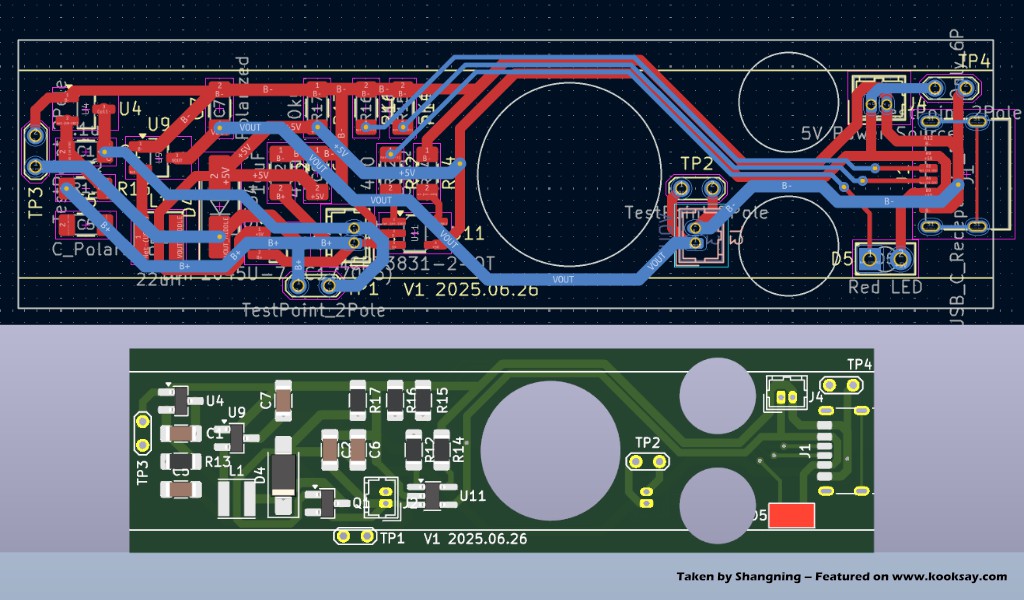
The Power PCB For My Side Project Has Arrived
06/30/2025 at 18:39 • 0 commentsSome basic components such as resistors and capacitors have not yet arrived. Once all the ICs are in hand, I will proceed with soldering and testing to see if it performs as expected.
![]()
![]()
-
Improvements To the Charging Power Part of 1×2 Audio Switcher
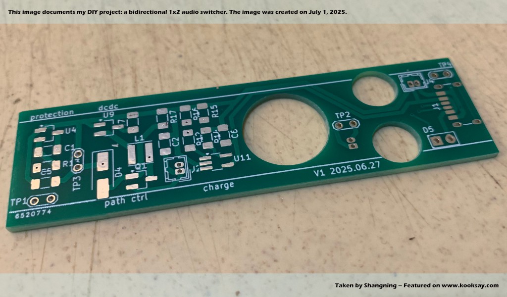
06/29/2025 at 15:24 • 0 commentsI submitted the V1 of the power board to the factory for PCB fabrication. Although it will still take a few days before I receive the board, I’ve already started working on the adjustments.
In the initial design, there didn’t include TVS protection for the Type-C connector, since I wanted to quickly verify the core functions. But today, I’ve added that section — it’s actually quite simple, requiring only a single TVS diode.
To make hand soldering easier, I avoided the commonly used ESDA25P35-1U1M due to its packaging being unfriendly for manual soldering. Instead, I chose the SMF5.0CA, which has a large enough footprint to make hand soldering more convenient.
As for the LED indicators, they’re relatively more complex. That’s because the charging chip I’m using, the MCP73831-2, only provides a single STAT pin. The typical application diagram from the datasheet shows only one indicator LED. Fortunately, this pin can output three different states — LOW, HIGH, and HIGH-Z — which makes it feasible to drive two indicator LEDs.
In the modified circuit, I’ve used a bi-color LED package (one housing both red and green LEDs), along with a logic gate circuit. This allows the red LED to light up during charging, and the green LED to light up once charging is complete.
I won’t be show the related schematics for now, as I prefer to wait until I receive and test the V1 board. After identifying any issues and making the necessary adjustments and improvements, I will then release the complete V2 circuit for the button cell charging section.
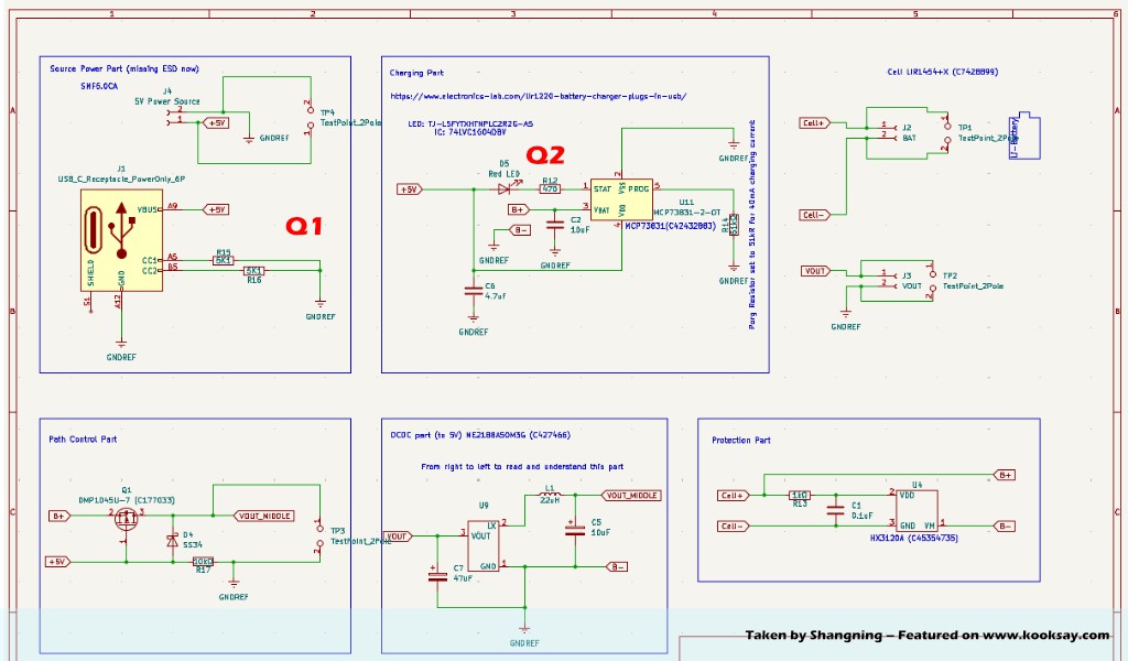
Below is the schematic diagram of Version 1, with two areas marked in red that are either in need of improvement or currently being improved.![]()
-
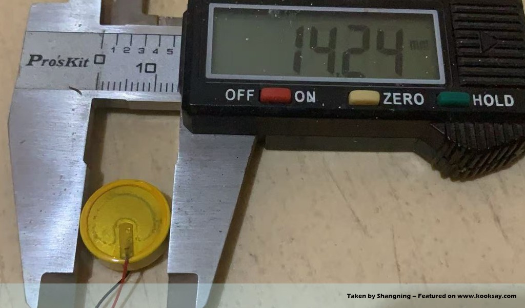
Battery Size and Type
06/26/2025 at 10:02 • 0 commentsConsidering the limited space, large batteries cannot be used, so I decided to use the Lir1452 coin-type lithium battery. This battery has a capacity of approximately 85mAh, which makes it unsuitable for more common and mature battery charging and management solutions. Fortunately, there are solutions specifically designed for small-capacity batteries, and today I’ve drafted the initial circuit.
![]()
I’m currently considering using the MCP73831 as the charging IC because it allows setting the charging current between 10–40mA, which is relatively safe, battery-friendly, and suitable for my current cell. In addition to the charging section, the Power Part also needs to handle path control, battery protection, and DC-DC boost functions. As a result, the space that initially seemed sufficient is now starting to feel a bit cramped.
Additionally, since I don’t have prior experience with the overall functionality, I’ve added several test points to the circuit to ensure easier debugging during the initial stages. These test points will help inspect various sections and troubleshoot potential issues more conveniently.
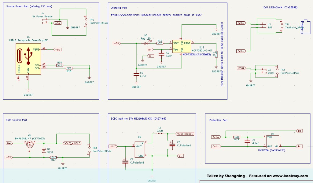
Based on reference materials from more mature solutions and my understanding of the currently selected ICs, the circuit schematic is:
![]()
Since this circuit requires manual soldering, large ground fills have been avoided to ensure ease of soldering. Additionally, all ICs use larger package sizes where possible, and the pads are designed for hand-soldering, which should help make the soldering process more convenient.
Of course, the overall layout and placement of the ICs may not look very tidy at the moment, but my priority is to first verify the functionality of the circuit. Once the functionality is confirmed, I will revisit and refine the IC placement and routing to improve the overall organization.
![]()
The soldering and testing will be completed next week.
Bidirectional 1×2 3.5mm Audio Switcher
Compatible with 3.5mm TS, TRS, TRRS Audio Jacks