RamBros
Circuit explained:
View the Simulation on TinkerCAD
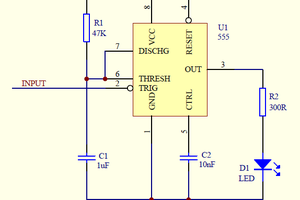
1) 555 in Astable mode
This constantly keeps switching and generates a square wave signal at the output.
- Time period: ~1.35s
- High Time: ~1.2s
- Low Time: ~0.15s
2) 555 in Monostable mode
This generates a single square at each falling edge of its TRIG pin. This is a high impedance input pin connected to the output of the astable IC.
- High Time: ~1.1s
The combined output (signal between OUT1 and OUT2) looks like a cardiac pulse when its RC smoothed.
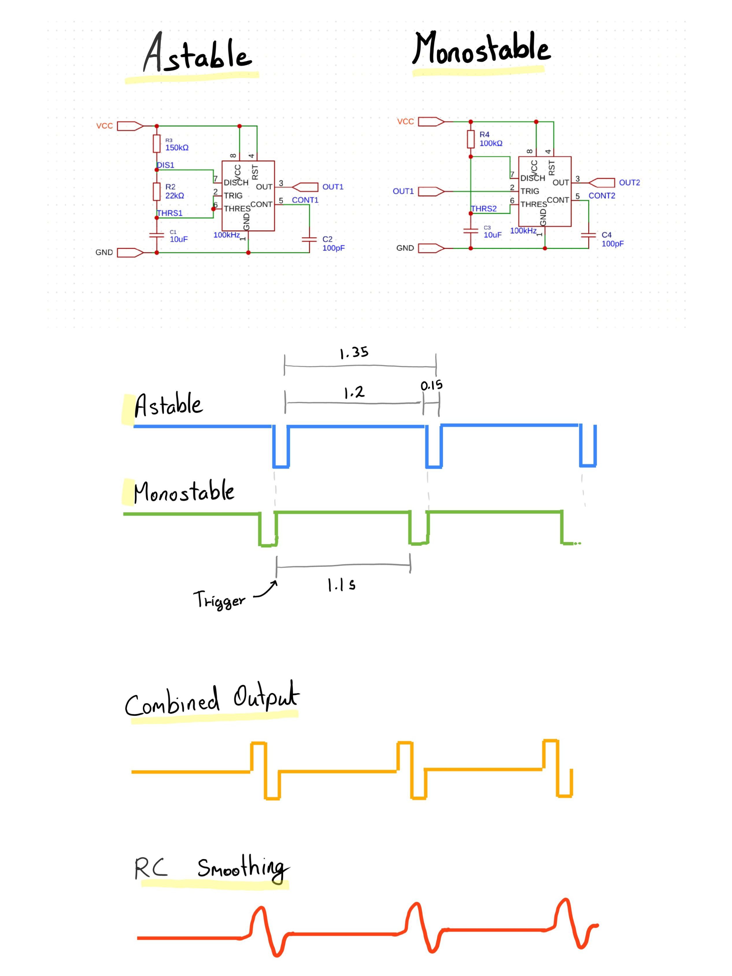
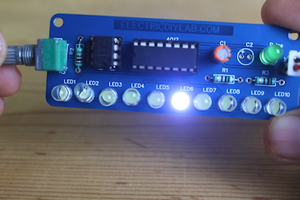
There are two sets of leds. The LED anodes (+) are connected to the Battery positive, the cathodes (-) to the 555 outputs. So the high time of the 555 output corresponds to the OFF state of the LEDs.
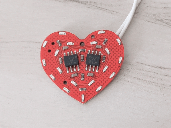
PCB Design:
The heart shape outline was imported from an SVG file. This is a basic 2 layer board, designed to be aesthetic and eye-catching.
The top side has the blinking circuit, the bottom side has footprints for a slide switch and a 1632 battery holder.
Notes:
- This design is optimized for jlcpcb smt service. Uses only basic components.
- The 555 used here is rated for minimum 4.5V supply voltage. But here it works at 3.3V - 4.2V; this type of off-spec usage is not suitable for production designs.
 sandy
sandy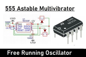
 Lithium ION