Continuation of a recent project
A couple of months back, I published a project on hackster.io (and source code on github) which involved a great level of manual size optimizations to create a blinky for STM32F4 discovery board with compiled binary less than 50 bytes in size. This work is highly inspired from 100 Bytes Blinky Challenge on Segger Blog.
It is recommended to refer both of these before continuing further. Description below extends the same project to reach much closer to 1Hz, while still keeping the size less than 50 bytes as before.
Summary of optimizations carried out so far
It is strongly recommended to refer to the hackster blog port, however below is the list of optimizations carried out till delay_blinky_09 example in github repo :
- Not using the startup code, instead writing application directly in Reset_Handler. Omitting the startup code restricts the variables to stack memory (local variables) only, because there is no startup code to perform copy of .data section and initialize .bss sections.
- Not using stack memory and storing the local variables in arm cortex m4 core's general purpose registers. This limits the number of variables up to the available general purpose registers. This is achieved by declaring local variables with register keyword.
- Using Bit-Band for peripheral register read/write/modify. Normal read-modify-write way requires more instructions to perform atomic write operations on individual bits of any peripheral register.
- Declaring Reset_Handler as naked function, so that function prologue/epilogue are not generated by compiler. This is fine because we are not calling any functions or performing any stack operations.
- Removal of initial stack pointer from vector table (since we are not using stack) and starting it directly from the reset vector. It requires vector table to be loaded with offset of 4 bytes to cater the missing initial stack pointer.
- Caching address of GPIO IDR (Input Data Register) and GPIO ODR (Output Data Register) to general purpose registers, so that same address is not read from ROM each time a write is done to ODR. This can be considered a speed optimization and not specifically a size optimization.
- Using Bitband allows to use NOT (mvns) instruction to toggle a bit in ODR, instead of using XOR (eor) instruction which takes 2 bytes more.
- Reusing the same register variable for different writes to different peripheral registers during initialization.
- Preferring instruction which use immediate load instead of load from a ROM location. This constrains the values to be loaded to few significant digits only, or else will result in load from ROM location instead of immediate load.
The delay required for toggling LED at 1Hz is achieved using blocking software delay, which involves counting to certain number for spending (wasting) given delay time. Therefore, with implementation of each new optimization, the code execution time changes based on the instructions generated by compiler. Hence, it requires tuning the delay value by trial and error so that resultant blink frequency is closer to 1Hz.
Where do we stand, how much closer to 1 Hz ?
delay_blinky_09 uses a delay value of 2097152 (2^21 or say 1<<21) to be compared against counter for toggling the LED. This value was chosen as it is a natural power of 2 and hence allows immediate load instruction to keep size below 50 bytes. Below is the waveform at Red LED (PD14) for this example (taken using 24MHz logic analyzer).
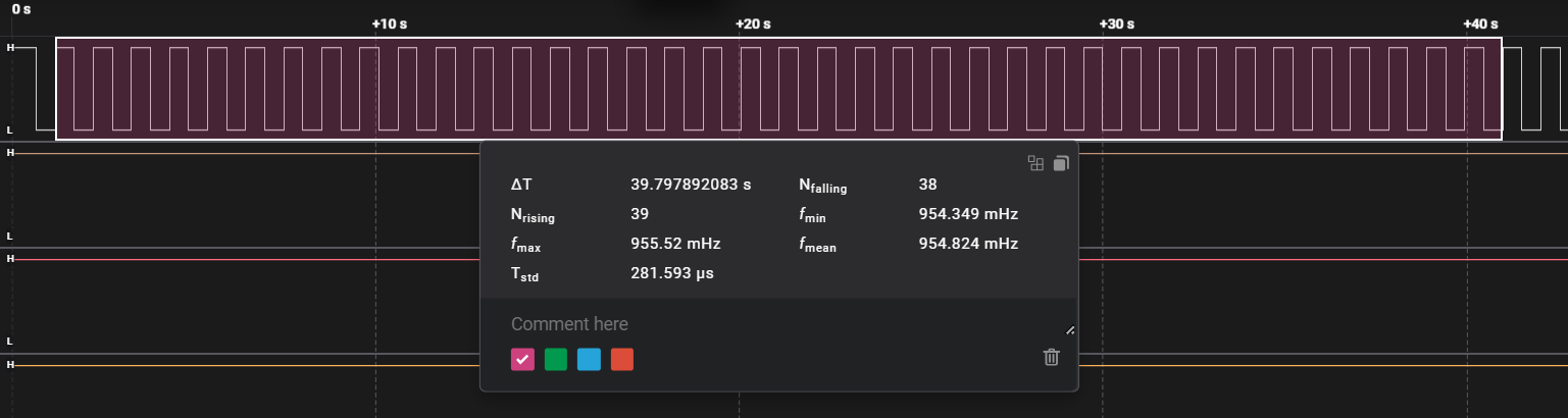 Hence, with reference to logic analyzer's 24MHz clock, this blinky is 0.955Hz (0.954824 Hz). This is approximately 0.045Hz error, small but significant.
Let's improve (a little)*
delay_blinky_09 has blinking frequency slightly less than 1Hz, meaning that it is a little bit slower and hence seems like we are counting a bit more than required for delay. Hence, by trial and error I found a delay value of 2015232 (1111011 << 14), which still uses immediate load instruction...
Read more »
 aaron
aaron
 Erik Piehl
 Charlie Smith
 agp.cooper