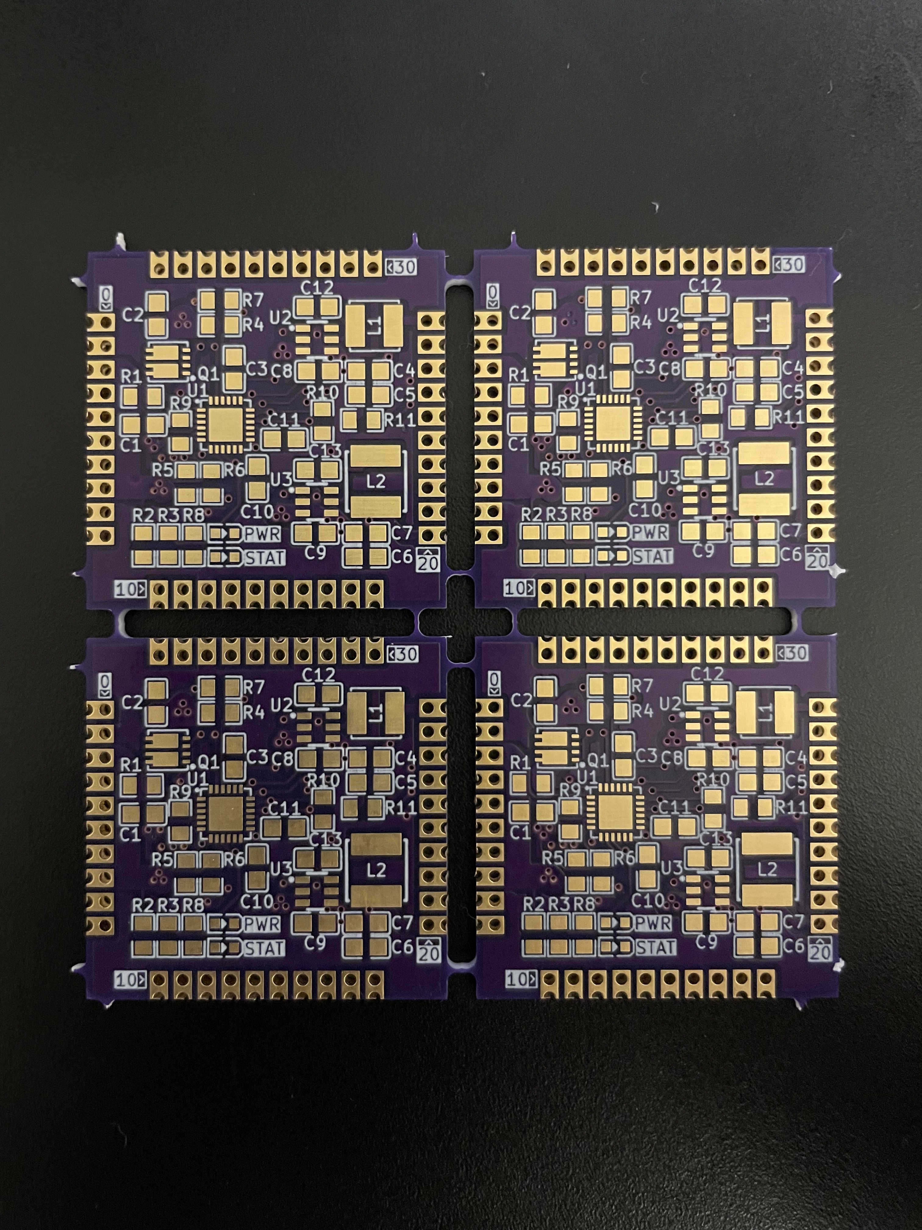
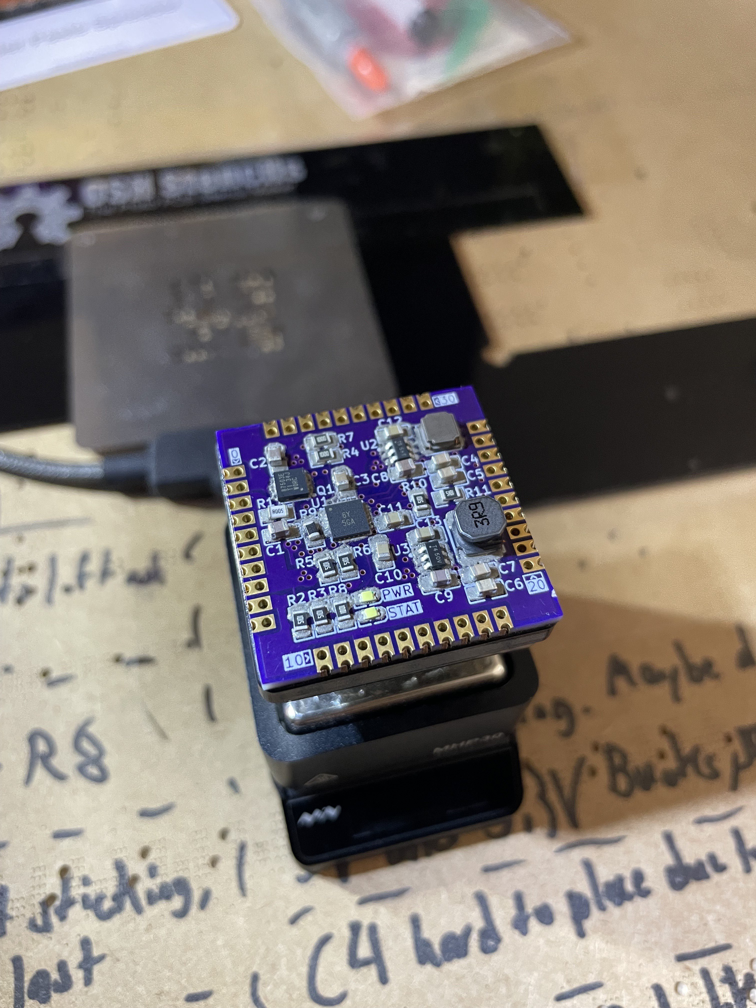
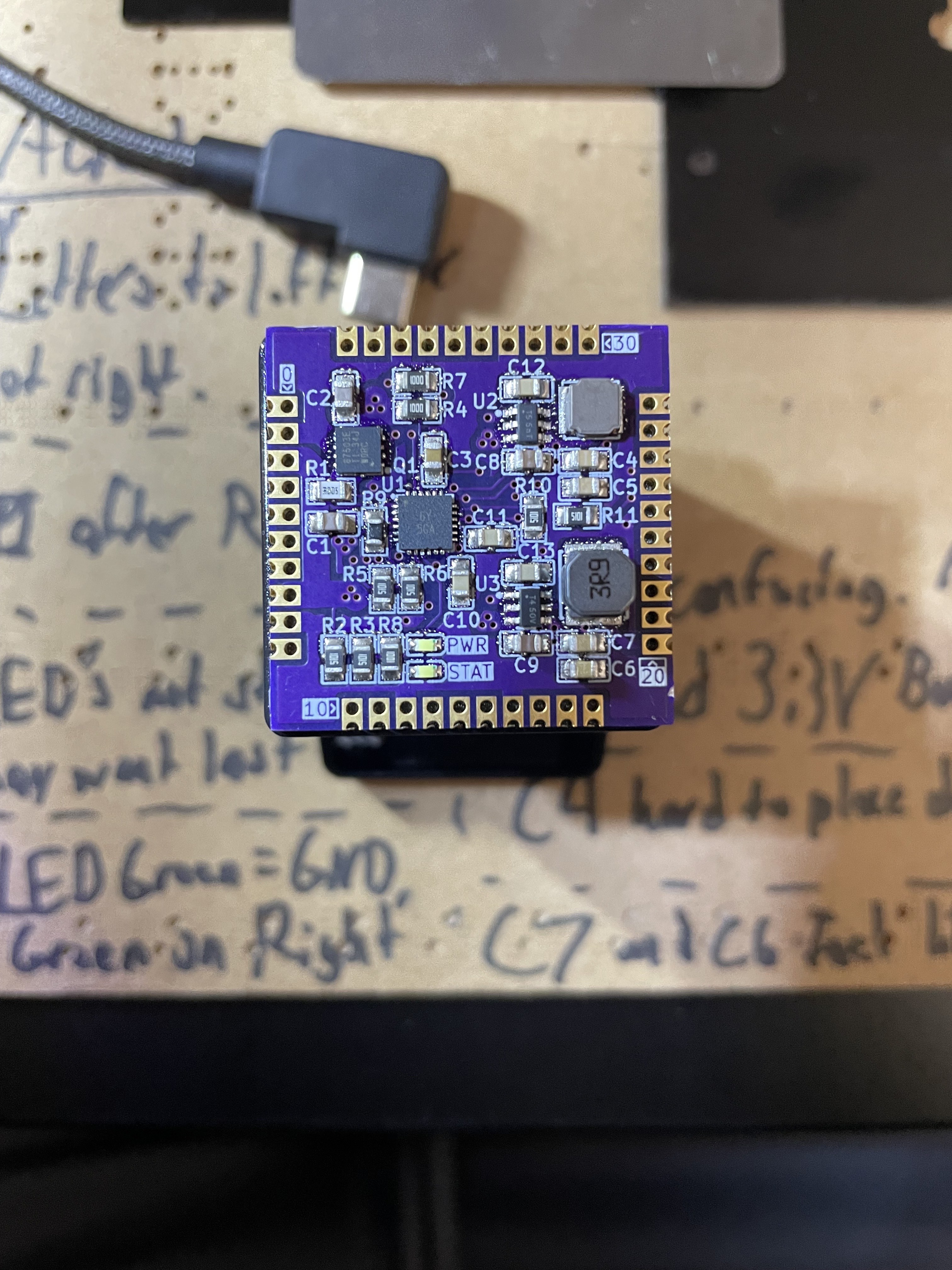
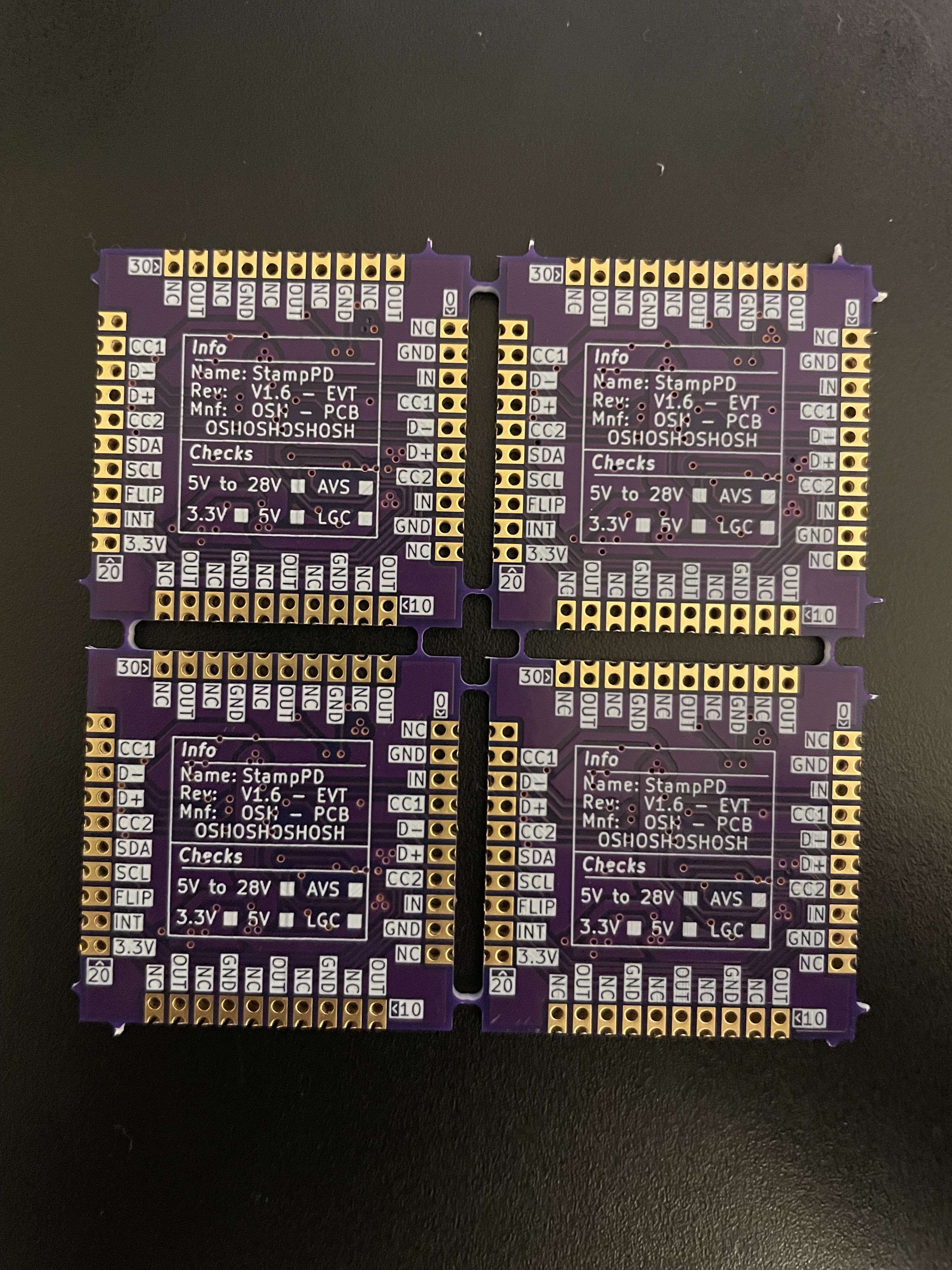
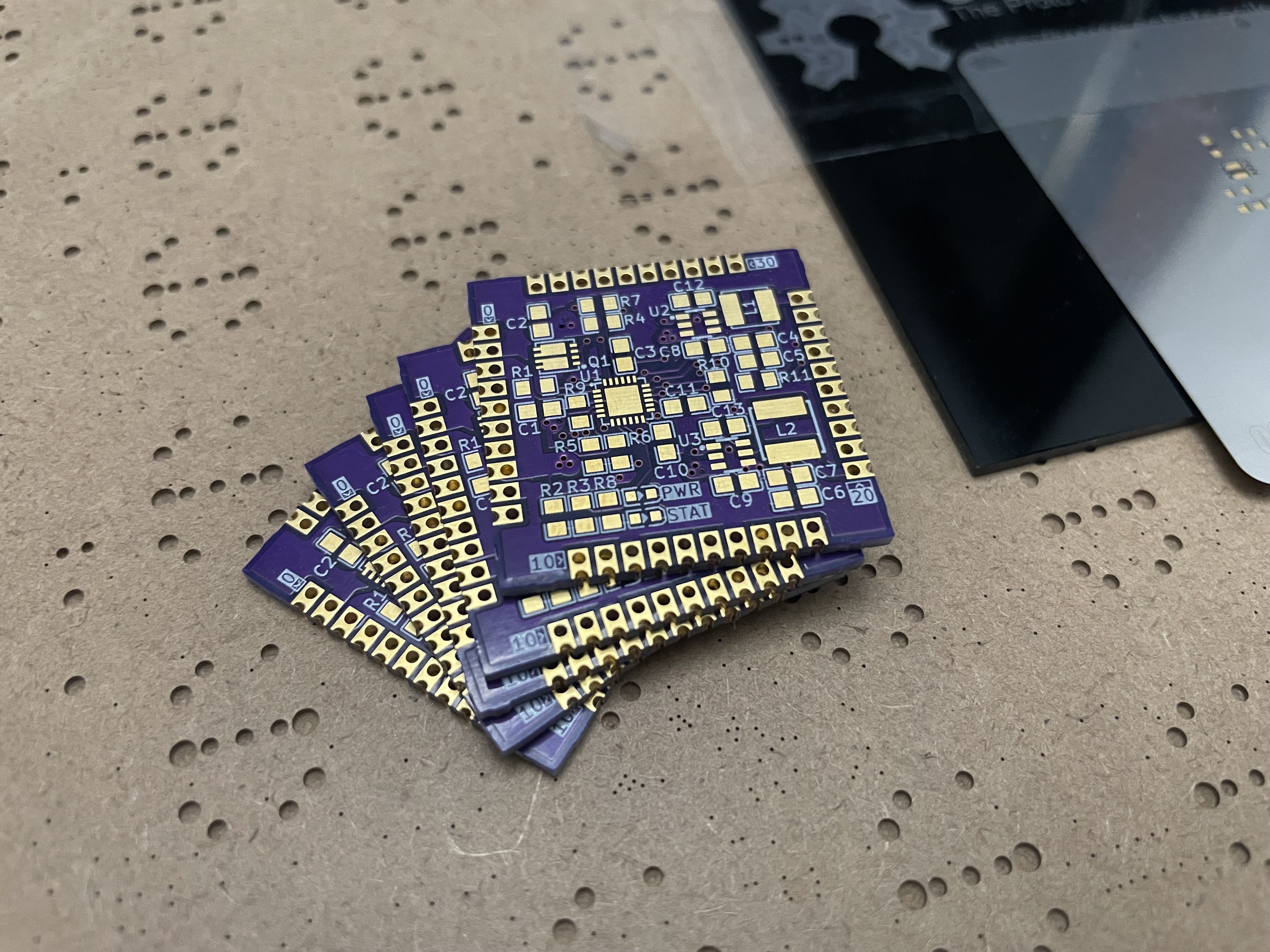
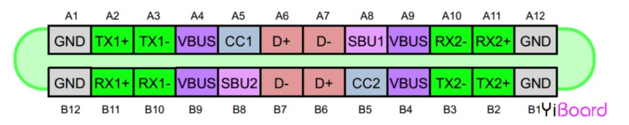
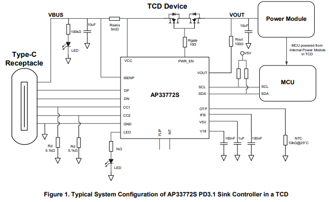
A PCB stamp to add 140W Power Delivery 3.1 (PD3.1) to any I2C capable microcontroller!
To make the experience fit your profile, pick a username and tell us what interests you.
We found and based on your interests.
Hello all!
It's been a second since the last log. I have been busy with end of the year plans and have finally come back to this project. Progress has not stopped while I was away though!
In this log I'll go through my methodology when ordering EVT (Engineering Validation Test) Components and PCBs, reasoning for chosen Component Suppliers and PCB Fab, and some changes to the PCB as a result.
Sneak Preview of the PCBs!
My goal for EVT is to test the PCB and Components to make sure StampPD works correctly. I also want to validate some cost cutting decisions for the PCB that will be explained below. For the EVT iteration I will be hand assembling PCBs to get an understanding of component assembly issues, silkscreen confusion, and to make any necessary PCB fixes easier. My target quantity of StampPD EVT boards is 10 working prototypes but I ordered Components/PCBs for 12 boards to account for mistakes, broken components, and potential destructive testing.
The conclusions from the "DIY Component Cost Comparison" log have remained the same. I ordered all passive components from LCSC and 4 IC components from Digikey. The total cost of components can be seen below:
One decision that has changed from past logs is the PCB Fab. Originally I was planning to use JLCPCB or PCBWay as they were the cheapest based on my calculation of x100 PCBs. However, JLCPCB and PCBWay had additional tariffs well over $200 at the time I was ordering PCBs. Instead I used OSHPark as my PCB Fab and OSHStencil as my Stencil Fab since they are an American company and do not have tariffs. OSHPark was originally not considered in the "PCB Fab Cost Comparison" log due to their limited PCB options. The cost increase from the tariffs helped spur on some of the PCB changes below to manufacture the PCB with OSHPark. The total cost of the PCBs can be seen below:
In the "PCB Trace/Via Calculations and 2 vs 4 Layer PCB" log I chose 2 oz/ft^2 for the top and bottom layers of the PCB as it allowed for smaller trace widths. OSHPark 4 layer boards only have the option for 1 oz/ft^2 top and bottom copper thickness and 0.5 oz/ft^2 middle layer copper thickness. This increases the Trace Widths of the design!
With the decrease in copper thickness, the Trace Widths on the Top and Bottom layers needed to increase. To facilitate this, I moved the 5A net to Top layer and 4A net to Bottom layer. The 2A traces remained on the Bottom layer like before. This minimized the size impact of these traces and allowed for the PWR layer to be an unbroken plane. Shuffling some components and traces around allowed the PCB to remain the same 30mmx30mm size constraint.
When looking at the manufacturability of the PCB, I realized just how big the 1.2mm Via Hole Size was for the 5A and 4A nets. These holes takes up a lot of space and could cause shorting issues. To resolve this, I replaced the 1.2mm Hole Size with x3 0.4mm hole size. This reduced the number of drill sizes need to 2 and allows for all Vias to be tented at the cost of more drilled holes per PCB. They should be able to carry the same amount of current.
As I assemble and test the EVT PCBs, I will be keeping an eye on the PCB thermals....
Read more »Hi all,
I've put together a DIY component cost comparison for StampPD. My goal was to understand how much per component StampPD would cost, see if there are any optimizations I could make, and figure out where to source parts. This will eventually be contrasted with PCBA services from fabs like JLCPCB.
Similar to the PCB cost comparison, I have selected 100x PCB's as my target amount for price analysis. This gives us most of the bulk component cost advantages while matching the PCB comparison. I will only show the prices for 100x PCB's. If there is more than one component per PCB, I will buy multiples of 100x for the component (Ex: There are 4x 100nF capacitors in each StampPD so we'll need 400x of them for production runs). If we cannot buy components in the exact amount needed, we'll buy the next largest quantity. I will not be including any replacement components in this calculation to fill for any lost/broken/destroy components that may happen in the production process. Any extra components due to quantity oversizing is not purposeful.
I will be looking at 3 main suppliers: LCSC, Digikey, and Mouser. These were selected as they are 3 that I am most familiar with. Not all parts could be found at all 3 suppliers. I am open to other suppliers so feel free to send a DM if you have suggestions. I use https://octopart.com/ to check for better prices for components as well but generally found better prices were only at suppliers that I did not know or trust.
The last columns also calculate the price by multi-sourcing the cheapest components across suppliers. There are two summary sets of data for each column, the Sum Cost and the Per Board Component Cost. The Per Board Component Cost is the more important value here as it helps to inform the price of the final StampPD boards. There are two variations of these values, one without shipping, tax, and tariffs and one with. The multi-sourcing column estimates the combined shipping, tariffs, and tax from ordering from more than one source.
Here is the price comparison for 11/18/2025. Note that prices can and have changed over time
Since this log is being written a bit late, I've already performed a second pass of the component cost comparison. Some changes below are:
Hi all,
In this log I want to go through the cost estimates for a couple PCB fabs. The routing for the PCB is far enough along now that I can put in all the settings we need to get cost estimates. This helps to give me an idea of what costs to expect for the final product.
I am targeting 100 boards as it is an ideal target for hitting cost savings when buying components in bulk and seems like a reasonable amount of boards to make that they wouldn't sell out instantly.
StampPD is initially designed around JLCPCB as the PCB manufacturer. This is due to 2 reasons: I have experience with them in the past and I wanted to try JLCPCBA service. If any specs seem a bit arbitrary, it is likely that this is JLCPCB's default capabilities. For some specs like the Copper Weight, please see the last log. For all PCB Fab quotes, I will select the following specifications:
Any specifications not listed above are not very important to the StampPD design at this time. That means specs such as these will be selected to be as cheap as possible: Surface Finish, Layer Stackup, Via Process/Covering, PCB Thickness, PCB Color, Silk Screen Color, and Board Outline Tolerance.
A website which lists PCB fabs for small batch production can be found at BuildList.org. I filtered this list to Fabs that allowed me to select the above settings. This removed some Fabs, such as OSHPark, as they did not have settings for 2 oz/ft^2 Copper Weight for 4 layer boards or Castellated Holes. I also removed any discounts given as these may not be repeatable on subsequent orders. Note that prices may fluctuate depending on the time and place of your order. This leaves us with the resulting quotes as of 11/25/2025:
As you can see JLC, AllPCB, and Elecrow are the cheapest. PCBWay and SEEEDStudio are more expensive but still somewhat reasonable while Eurociruits is completely unreasonable. For now, I plan to stick with JLC unless prices change drastically.
Below are screenshots of the prices given above:
Hi all,
This log will go through the calculations required to size the traces and vias for the StampPD PCB as well as the decision to move from a 2 layer board to a 4 layer board.
We need to calculate what copper weights are required for the PCB based on the max expected current through traces and vias. For StampPD, we have 4 power domains that have significant current. These are:
While the buck converters for 3.3V an 5.0V can output up to 2A of current each, they require a different amount of input current. To calculate each buck converters input current, we multiply its Max Output Voltage by the Max Output Current then divide that by the Minimum Input Voltage times the Efficiency.
The minimum Input Voltage for both buck converters will be 5V as this is the minimum voltage defined by USB. The efficiency can be found in graphs for the AP63200 but no 5.0V input voltage line is given. For now I'm taking the 12V input voltage efficiency at 2A which is around 90% for both buck converters. The actual efficiency is likely higher than this as efficiency in a buck converter increases as the input and output voltages are closer in value. By replacing the equation values and adding both buck converters input current requirements together, we get the below solution:
This gives us 3.7A which I round up to 4A for safety margin.
KiCAD has built-in "Track Width" and "Via Size" calculators that I'll show here. To start with, lets look at the 5A domain with default 1oz copper weight at 10C temperature rise for around 30mm conductor length ( length doesn't change track width much here so we'll default to 30mm since this is the length of the PCB ).
This gives us a 2.81mm trace width for external layers. For a 30mm x 30mm board, this is huge! This trace alone will take 1/10th of our board space in a single axis at a minimum! Reviewing the data sheets for all IC's, we can increase the temperature rise to 20C safely for all of our components with minimal loss in efficiency to get a trace width of 1.85mm. This is still quite large and doesn't provide enough routing flexibility. This leaves one last thing to change which is the Track Thickness, also known as Copper Weight. By changing this from 1 oz/ft^2 to 2 oz/ft^2, we get a track width of 0.92mm.
Rounding this trace width up to 1mm gives us a bit of a safety margin and is easier to keep track of. Increasing our Copper Weight to 2 oz/ft^2 will increase the price of the PCB but there isn't much choice if we want to support 5A. Note that a 1mm wide trace width for 5A is only valid for PCB layers that are external ( top and bottom layers ). Internal layers will need much thicker traces as they usually have lower Copper Weight, usually 0.5 oz/ft^2, and can't remove heat as easily.
Since the temperature rise and copper weight are set by our 5A traces, we can calculate the trace widths needed for 4A and 2A as 0.7mm and 0.3mm as seen below:
When calculating the Via Size, we can use the 20C temperature rise from the above calculations. We should be careful to not confuse the 2 oz/ft^2 copper weight with the plating thickness of the Via. Using JLCPCB's default capabilities, we can see that the "Average Hole Plating Thickness" is 18um. Keeping all other parameters default in KiCAD, including the default Via Hole Size of 0.4mm, gives us a Via that can support up to 2.4A:
While this will be sufficient for the buck converter 3.3V and 5.0V 2A output domains, the VBUS 5A domain will need larger Vias. Going up by 0.1mm steps, we can arrive at a 1.2mm Via Hole...
Read more »Hi all,
I was at Hackaday Supercon 2025 and did a quick 7 minute lightning talk about this project! You can watch it here, timestamp is exactly 1 hour into the video!
I'm continuing to finish the routing and have a couple of logs that will be forthcoming:
I'm planning for logs past these such as prototype feedback and software library implementation but those are further out. Once I order prototypes I plan to release the initial Gerber, Step, and BOM files for JLCPCB.
Note that I will be busier as the year comes to a close so this project will slow down until January 2026. I hope to order the prototypes before 2026 but that is up in the air.
Hi all,
This log will describe what pins we need to define for the PCB package. Below is a list of all inputs and outputs:
The logic used to determine which side of the PCB pins should be on is to go from left-to-right when looking at the PCB from top down. The logic/power input is on the left side while the logic and 5.0V/3.3V power output is on the right side. The variable USB-C Power output is on the top and bottom. You can see this in the schematic diagram below:
As this stamp will use USB-C for power and data input, the most logical pin input routing should match the expected pinout for a USB-C Female Receptacle. Based on the image below, you can see that this leads to ground on the outside, then power (VBUS), CC Pins, and finally USB D+/- .
The right side output pins on the stamp do not have a likely output order like the left side Input Pins do. As such, they are organized based on ease of routing and part placement. The 5.0V and 3.3V power output pins flank the top and bottom due to the placement of the buck converters for the associated voltages. Next are the communication pins for SDA and SCL and the PD Controller INT and FLIP logic pins. The SDA/SCL pins were placed on the top due to their necessary components needed for the SDA/SCL pins being located on the top while the INT and FLIP pins were closest to the bottom side of the PD Controller. Finally, the CC and USB D pins simply route from left to right across the PCB.
The top and bottom pin placement alternates between power output and ground pins, separated by a No Connect (NC) pin in-between. The NC pin was included to make it more unlikely that the power output pins and ground pins could be accidentally shorted when soldering StampPD. Its unclear if this is an optimal power pinout setup and would love feedback on this design choice.
Hi all,
In this log I'll go over the specific component selection for the USB PD Controller.
A USB PD Controller Sink is an IC that communicates with the USB PD standard to set a voltage and current from a USB PD source for downstream devices. The selected USB PD Controller for StampPD is the AP33772S. This IC comes in two variants , the AP33771C and the AP33772S. The C variant is a version which uses resistors to select the desired current and voltage while the S variant uses I2C to communicate with a microcontroller to select the voltage and current. In StampPD, we will use the S variant for its ability to change and request different voltages and currents. The controller selection was inspired by controller in the PicoPD which used an older version called the AP33772. This controller is Not Recommended for New Design (NRND) by the manufacturer, Diodes, and is only compatible with the USD PD3.0 standard. The AP33772S is compatible with the newer USB PD3.1 standard. I compared a couple differences between these two controllers in the Design Objectives log if you wish to see why this version was chosen. I attempted to research USB PD3.2 controllers that were similar to the AP33772S but was not able to find any, likely due to the standard being more recently released. Some reasons I've selected the AP33772S were:
Below, an example circuit, called Figure 1, shows what an implementation of the AP33772S should look like with some specified component values. A table called Pin Descriptions describe the functions and voltage / current for pins of the AP333772S. Since the circuit diagram + table gives us a good idea of what to implement for this IC, I'll describe the more important/complicated components and only put component values in a list for the others.
This resistor sits between ISENP (Current Sense Pin) and VCC. It is used by the AP33772S to determine the amount of IR drop through VBUS for overcurrent protection. Since VBUS supports 5A and the recommended resistance is 5mOhm, this resistor needs to support at least 5A^2 * 5mOhm = 0.125W ( P = I^2 * R ). We'll want to give around a 50% power margin here so our target resistor power rating is 0.125W * 1.5 = 0.1875W. We should also limit the resistance tolerance to within 1% to reduce variability and power loss.
This pin is described as outputting up to 5.33V, 2mA. If we use the suggested 1000Ohm resistance value, we should look for a LED with a Forward Voltage (Vf ) = Voltage Source - Resistor * Forward Current. Vf = 5.33V - 1000Ohms * 2mA = 3.33V. This means if we keep the suggested 1000Ohm resistor and assume 2mA of Forward Current, we should look for a LED with a Forward Voltage of 3.33V. This will likely be a blue or white colored LED.
This resistor is used to detect the temperature around the IC. When NTC resistors heat up, their resistance decreases. This can be detected to determine overheating conditions. For this IC, it's calibrated for a NTC resistor that has a resistance of 10KOhm when the temperature is 25C.
For the VBUS LED and Resistors, I'm ignoring the values suggested in the circuit diagram. Instead,...
Read more »Hello all,
In this log I'll go over the specific component selection for the 5.0V and 3.3V Buck Converters. Since I am using the same IC for both 5.0V and 3.3V, most of the components will be duplicated between the IC's. Only the inductors will be different between the two implementations.
The main buck converter IC is the AP6300. This IC comes in a couple different flavors including a 3.3V ( AP63203 ) and a 5.0V ( AP63205 ) version which I've selected for StampPD. Some reasons I've selected this IC were:
Below are the efficiency, load, and line regulation curves for the AP6300. Figure 4 shows the efficiency at different output current for 12V, Figure 5 shows the efficiency at different output currents at 24V. The blue line is 5.0V output, the red line is 3.3V output. Figure 6 shows the expected output voltage at different currents. The blue line is input voltage of 12V, the red line is input voltage of 24V. Figure 7 shows the expected output voltage with different input voltages. The blue line is output current of 1A, the red line is output current of 2A. From these we can take away a couple things:
I expect that for the 5.0V AP63205 I should see around 5.20V at low input voltage and low output current. As the input voltage and output current increase, I expect the output voltage to drop to just above 5.0V.
Using the efficiency trends in Figure 4 and Figure 5, I will guess that voltage for the 3.3V AP63203 will likely be worse (higher voltage at lower output currents and input voltages). Using the efficiency percentage difference of around 5% in Figures 4 and 5, and the voltage difference of around 0.2V from Figures 6 and 7, assuming this IC outputs 3.3V at around 2A 32V input, I calculate an output voltage around 3.3V + 0.2V * 1.05% = 3.51V.
I expect that for the 3.3V AP63203 I should see around 3.51V at low input voltage and low output current. As the input voltage and output current increase, I expect the output voltage to drop to just above 3.3V.
Below, an example circuit, called Figure 1, shows what an implementation of the AP63205 should look like. Two tables, called Table 2 and Table 3, show recommended component values....
Read more »Hi all!
In this log I'm going to go over my methodology for component selection. I will explain what subsystems I want to include on StampPD, component requirements, other influencing factors, and a summary of component restrictions. In the next couple logs I will go over each sub-system of the board component by component to explain my part choices. I hope to show how I went about component selection to give new PCB designers an idea of how I approached this this design as well as receive feedback from more experienced designers. I have minimal experience with power design so I'm sure I've made mistakes somewhere here!
There are 5 main parts of StampPD:
These 5 parts are combined together to create the stamp. Only two of these sub-systems are absolutely necessary, the PCB and the USB PD Controller. The USB ESD Protection is nice to have but is optional. Being only a single component (TPD4E5U06DQAR) it would be easy to remove. The 5.0V and 3.3V Regulators are also nice to have but could be removed if needed.
There are a couple requirements I've put on the design that influence what parts I want to select:
I have some personal external factors that also limit my part selection:
Here is a summary of the restrictions that I have put on component selection:
Hello everyone!
This is a quick update about my decision on the 5V and 3.3V regulators.
Last time I mentioned a couple methods for regulating the 5V and 3.3V which were:
I mentioned last time that I was planning to go with one of the Buck Booster options. However, I've changed my mind! Instead I'm going to just use Buck Converters
After thinking about these solutions for a while, I realized that the drop in voltage on the 5V pin when the input voltage is 5V is ok with my design choice for now. The reasons for this are:
For now I think simplicity and cost are more important than sacrificing a little bit of voltage here. I plan to test the 5V rail to see how much voltage drop we get and am leaving the door open on adding a Boost converter later. As a little bit of a sneak peak for next time, here's where the current KiCAD design stands!
Create an account to leave a comment. Already have an account? Log In.
Become a member to follow this project and never miss any updates
By using our website and services, you expressly agree to the placement of our performance, functionality, and advertising cookies. Learn More
Elia
hesam.moshiri
ElectronicABC
Kuba Sunderland-Ober