 Alec Probst
Hi all,
This log will describe what pins we need to define for the PCB package. Below is a list of all inputs and outputs:
- Input
- Power
- USB-C Port Power Input (VBUS_TYPEC)
- Ground (GND)
- Logic
- Channel Configuration 1 (CC1)
- Channel Configuration 2 (CC2)
- USB Data + (USB_D+)
- USB Data - (USB_D-)
- Power
- Output
- Power
- USB-C Port Power Output (VBUS)
- 5.0V, 2A Power Output (+5V)
- 3.3V, 2A Power Output (+3.3V)
- Ground (GND)
- Logic
- Channel Configuration 1 (CC1)
- Channel Configuration 2 (CC2)
- USB Data + (USB_D+)
- USB Data - (USB_D-)
- USB PD Serial Data (SDA)
- USB PD Serial Clock (SCL)
- USB PD Interrupt (INT)
- USB PD Port Flip Orientation (FLIP)
- Power
Pin Orientation
The logic used to determine which side of the PCB pins should be on is to go from left-to-right when looking at the PCB from top down. The logic/power input is on the left side while the logic and 5.0V/3.3V power output is on the right side. The variable USB-C Power output is on the top and bottom. You can see this in the schematic diagram below:

Pinout Reasoning
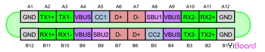
Input Pins (Left Side)
As this stamp will use USB-C for power and data input, the most logical pin input routing should match the expected pinout for a USB-C Female Receptacle. Based on the image below, you can see that this leads to ground on the outside, then power (VBUS), CC Pins, and finally USB D+/- .
Output Pins (Right Side)
The right side output pins on the stamp do not have a likely output order like the left side Input Pins do. As such, they are organized based on ease of routing and part placement. The 5.0V and 3.3V power output pins flank the top and bottom due to the placement of the buck converters for the associated voltages. Next are the communication pins for SDA and SCL and the PD Controller INT and FLIP logic pins. The SDA/SCL pins were placed on the top due to their necessary components needed for the SDA/SCL pins being located on the top while the INT and FLIP pins were closest to the bottom side of the PD Controller. Finally, the CC and USB D pins simply route from left to right across the PCB.
Output Pins (Top/Bottom Sides)
The top and bottom pin placement alternates between power output and ground pins, separated by a No Connect (NC) pin in-between. The NC pin was included to make it more unlikely that the power output pins and ground pins could be accidentally shorted when soldering StampPD. Its unclear if this is an optimal power pinout setup and would love feedback on this design choice.
Discussions
Become a Hackaday.io Member
Create an account to leave a comment. Already have an account? Log In.