Discrete Electronics Guy

Circuit Explanation
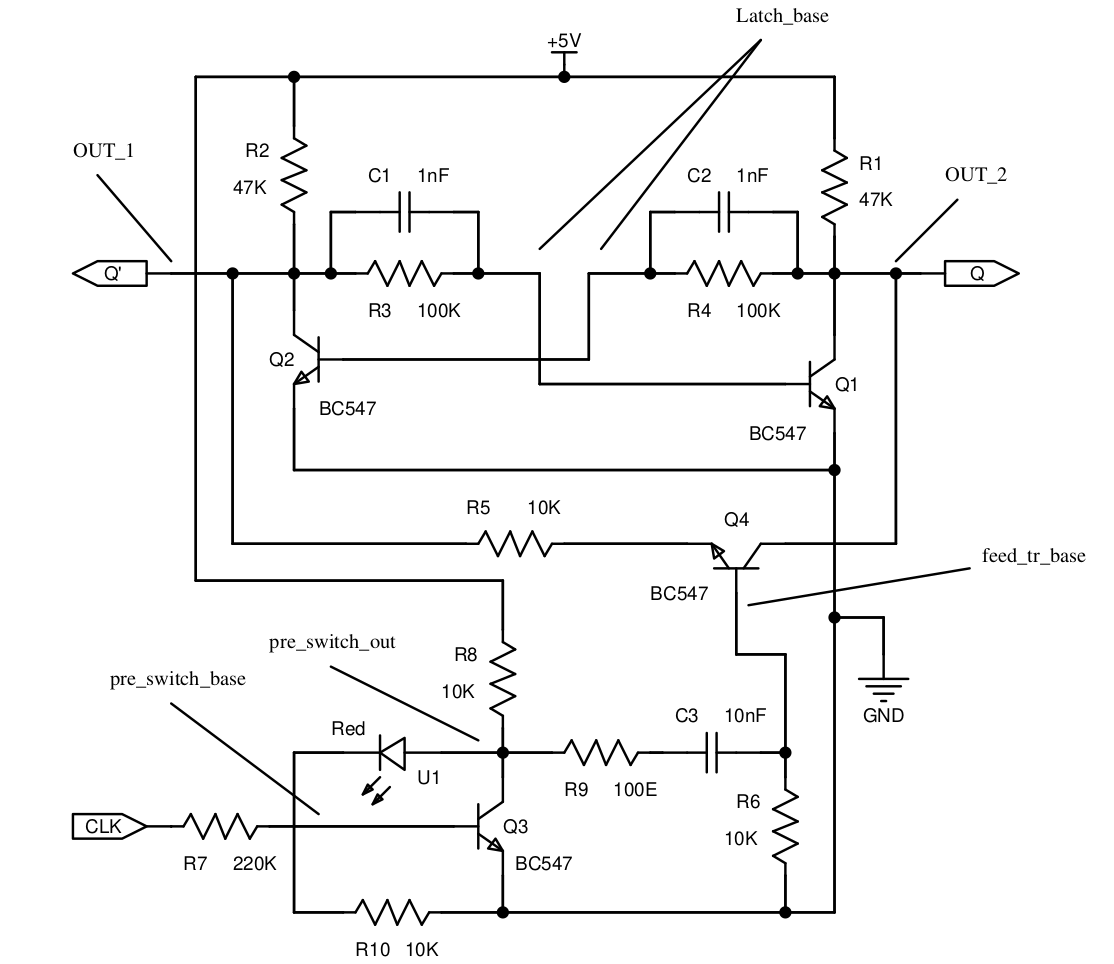
The circuit diagram is give below. I think the circuit is self explanatory. But I will explain in short. Basically the collector node voltage we are flipping using the feed_tr Q4 by connecting it between 2 collectors of the latch transistors Q1 and Q2. So, by flipping the state we can achieve the T flip-flop characteristics. The input control signal to the feed_tr Q4 is given by the pre_switch transistor Q3. This transistor is just to ensure that the input impedance is very high to make it possible to connect to other stages. This transistor Q3 output is then pass through a differentiator circuit using RC network to ensure that the flip-flop is an edge triggered. Because the differentiator convert the square waves into sharp spikes. So the Q4 will only turn on for a small interval. So this will effectively work as an edge triggered flip-flop. The collector resistors are keeping to a high value (47K) to reduce the power dissipation. The led U1 indicating the input clk status.
Output Analysis
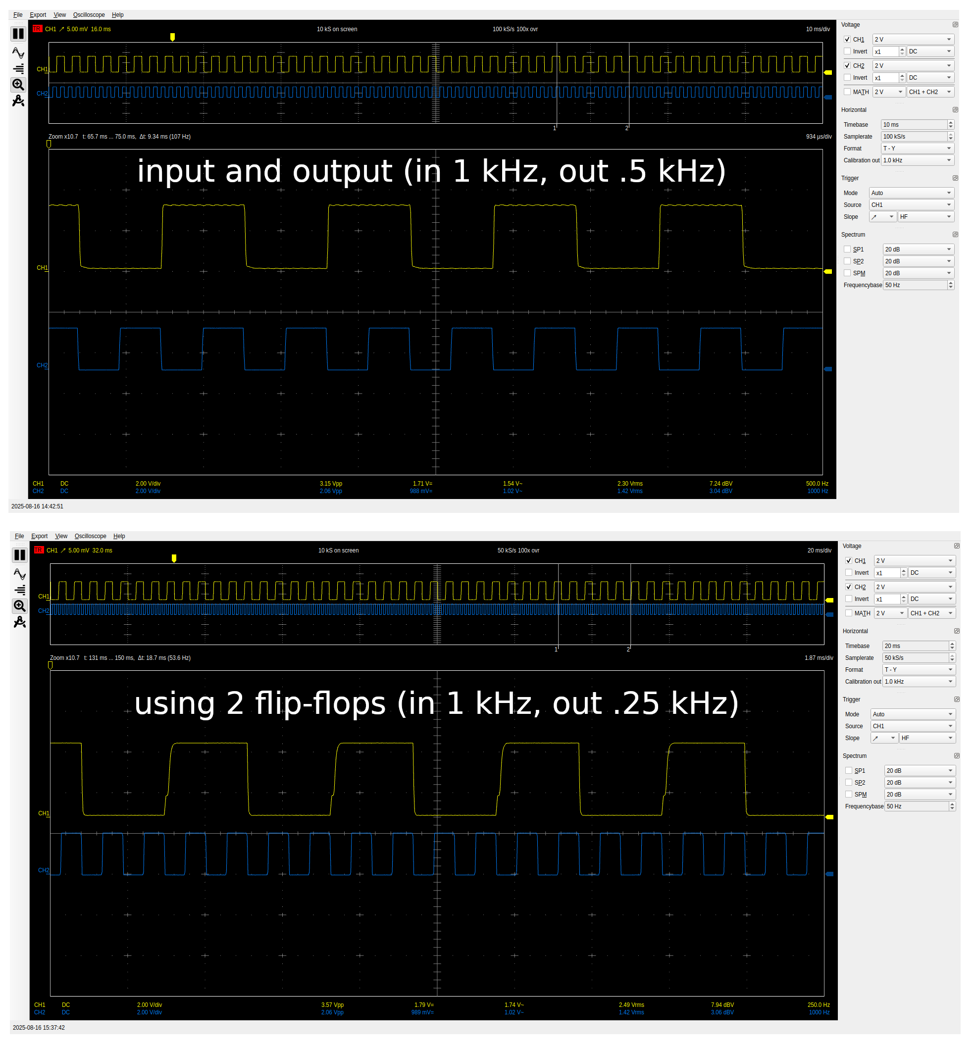
Here I am showing the output wave-forms of the flip-flop which I made. I am using a PC oscilloscope from "Hantek" to doing the experiment. I am using the calibration out of the oscilloscope as a signal input to my flip-flop. The calibration out frequency we can change from the PC interface. So I am generating different frequencies of square-wave and checking the circuit output. First image showing the output waveform by giving a 1 kHz input square-wave. The output frequency is divided by 2 after passing through the flip-flop. The second is showing the output of 2nd flip-flop after passing the 1 kHz through 2 different flip-flops. So the frequency again divide by 2 so the out become 250 Hz.
Note: Yellow is out and blue is input.
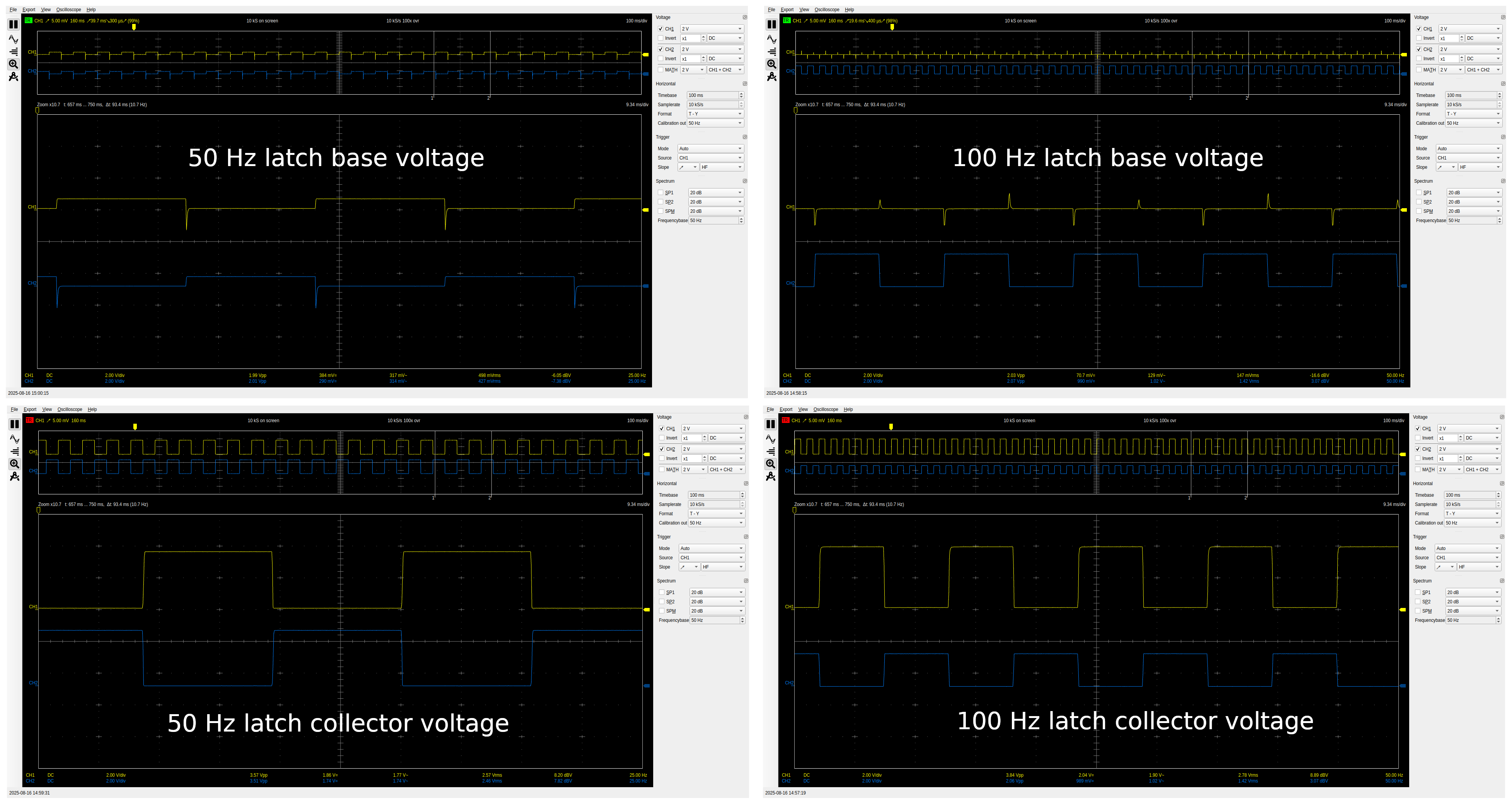
Here I am showing the output wave-form at the latch transistor base and collector point. I done the experiment for 50 Hz and 100 Hz. Both are attached in the below image.
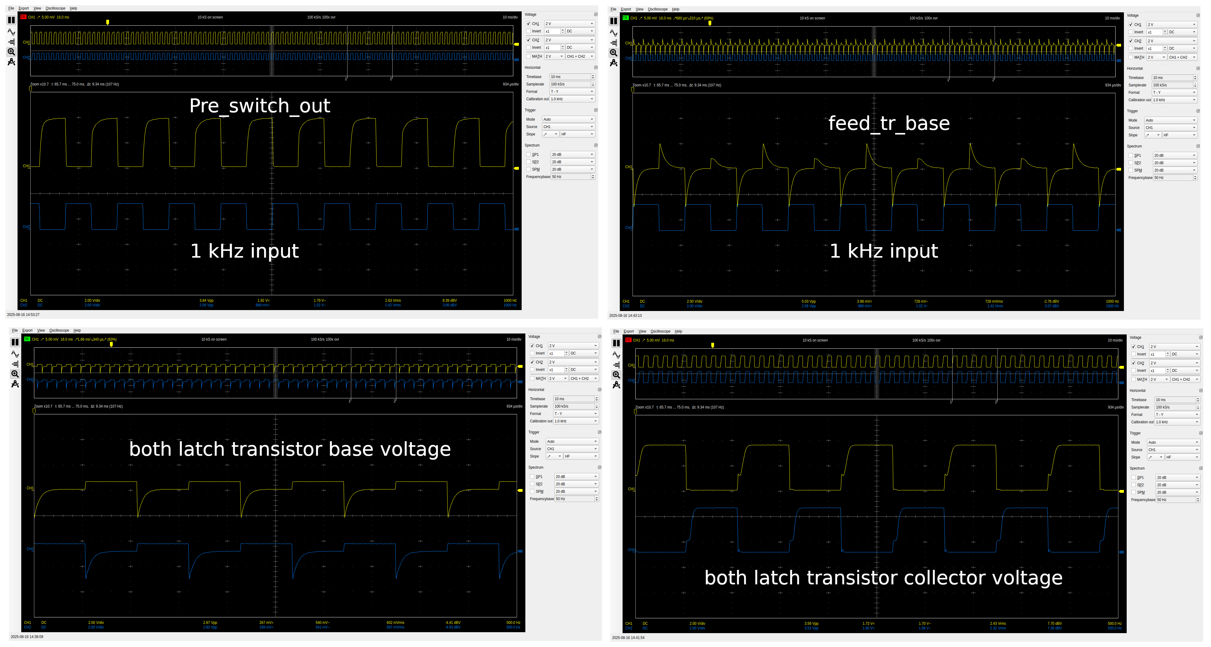
Here I am showing the wave-forms at more check points in the circuit by giving 1 kHz input square wave. The marked point you can find from the circuit diagram.
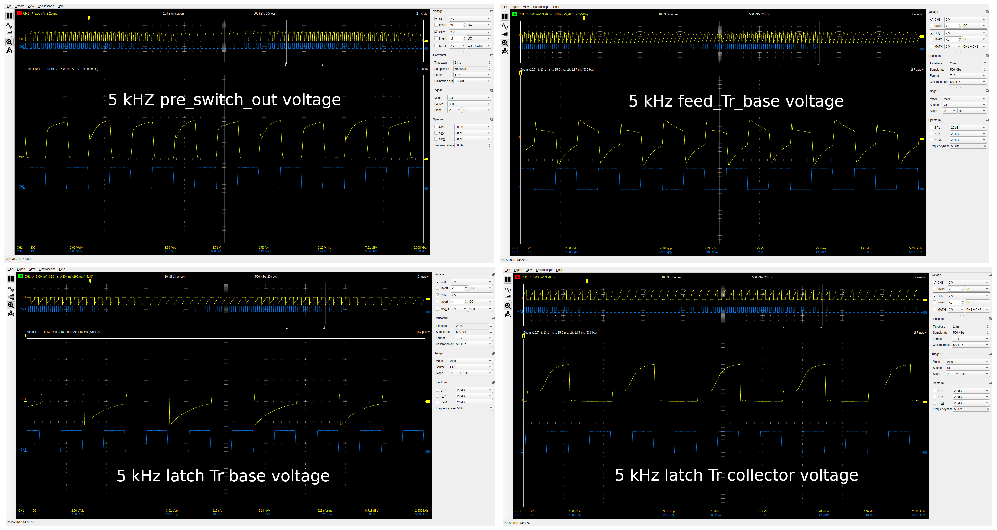
Here showing the same checkpoint waveform for an input of 5 kHz square-wave input. If frequency increasing further the circuit is getting failed. To improve for high frequency we need to reduce the capacitance value and the collector resistor value.
 MS-BOSS
 Jesse Farrell
 Frank Latos