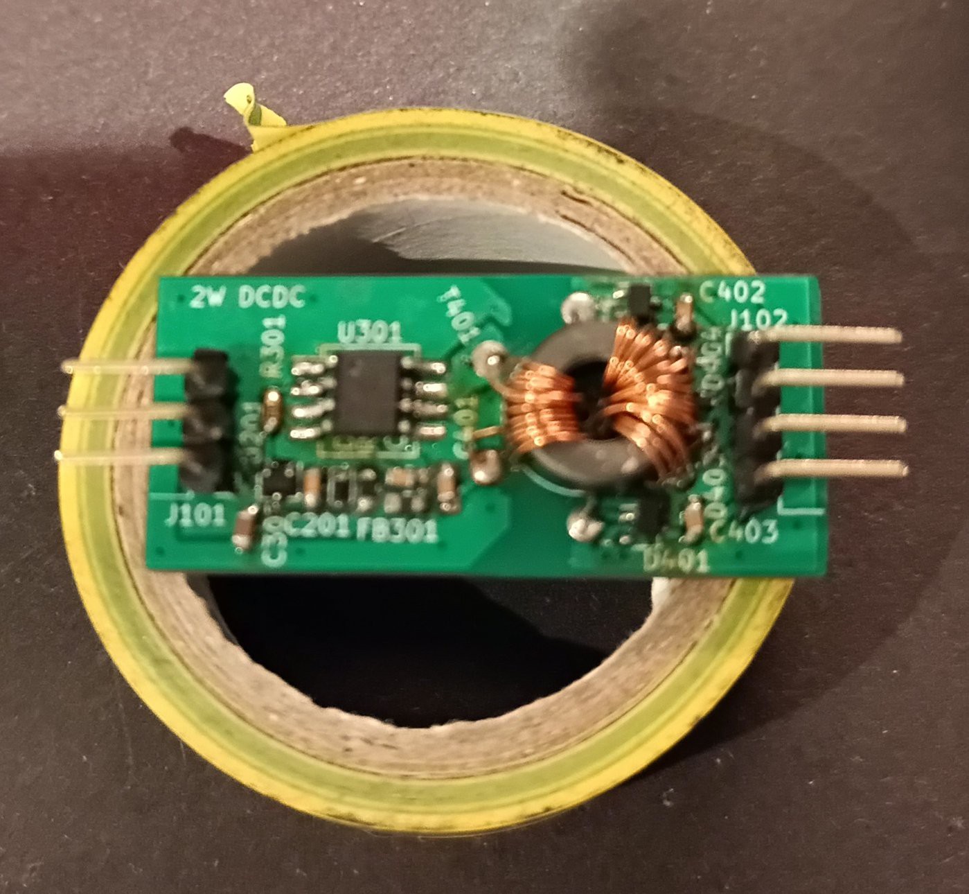
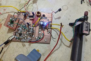
SIlicon Carbide FETs switch very quickly so they need very low capacitance gate drivers to limit switching noise on the control circuits (and EMC outside the unit). This is an experimental design of a gate driver to replace something like a Recom R12P22005D.
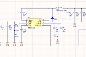
There's a fixed oscillator, a gate driver being abused as an H-bridge and a transformer with split output to give +15/-5V but output voltage depends on transformer winding and zener diodes.
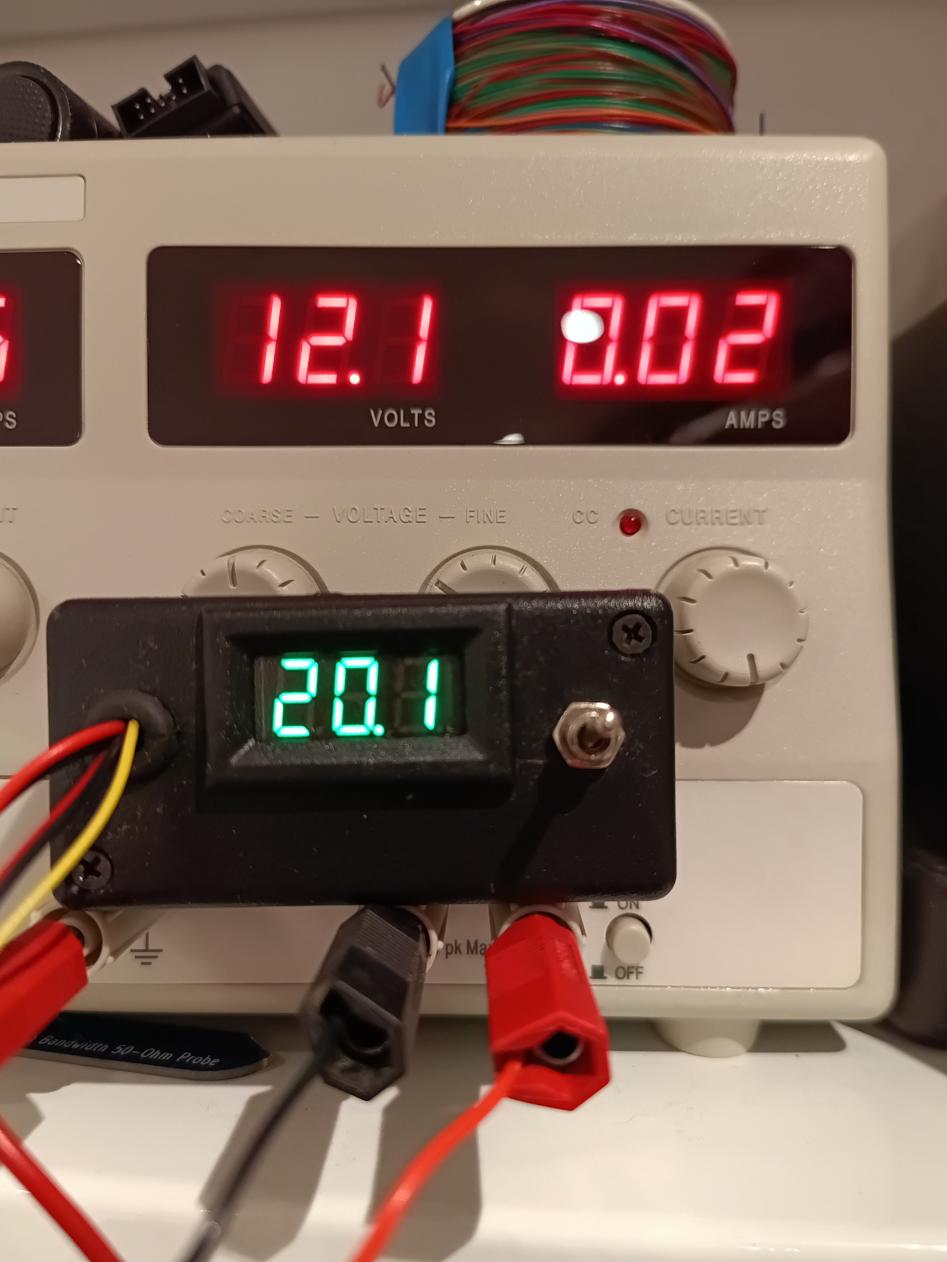
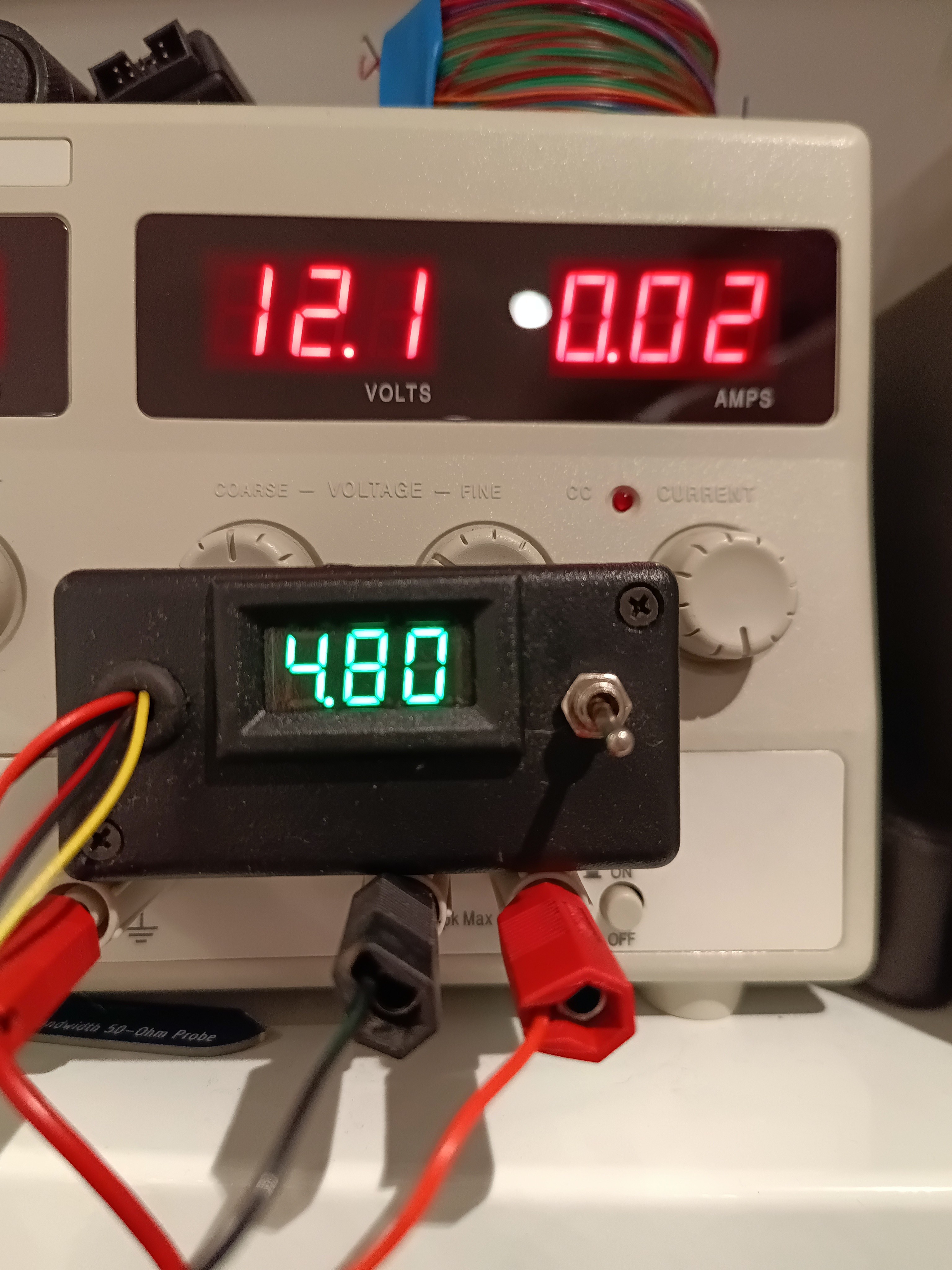
The project was successful but it's not a very efficient design or high power. It tends to give around 0.4W which is enough for most SiC TO-247 applications but a little more would have been nice (target was 2W).


 sadeed
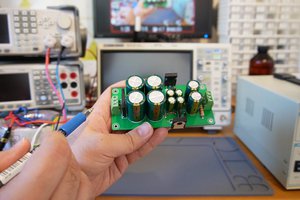
 hesam.moshiri
I went down a similar rabbit hole, trying to get a small +/- 15V supply for analog from 3.3V. One of the things I discovered was that my hand wound transformers did not perform well compared to commercial ones. Never figured out why.