-
exchange recent updates for working board
01/13/2017 at 16:48 • 1 commentIn the previous log it was shown that half of the ADC turned out to be non-functional. Luckily it wasn't the last board so another one was grabbed.
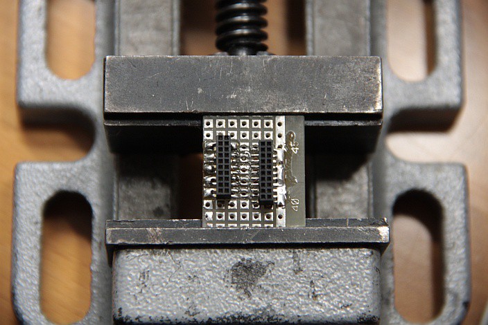
A few hours later we have a modified PCB with 1.27mm headers (perf board circles cut in half to yield 1.27x2.54 grid pads
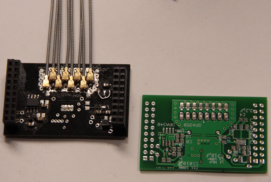
and thanks to quick delivery from China also a big pack of u.fl cables and connectors (sculpting the pads-to-be for U.FL was something that made me want to redo the PCB - Rev1E PCB on the right is for reference so you can see the GND polygon)
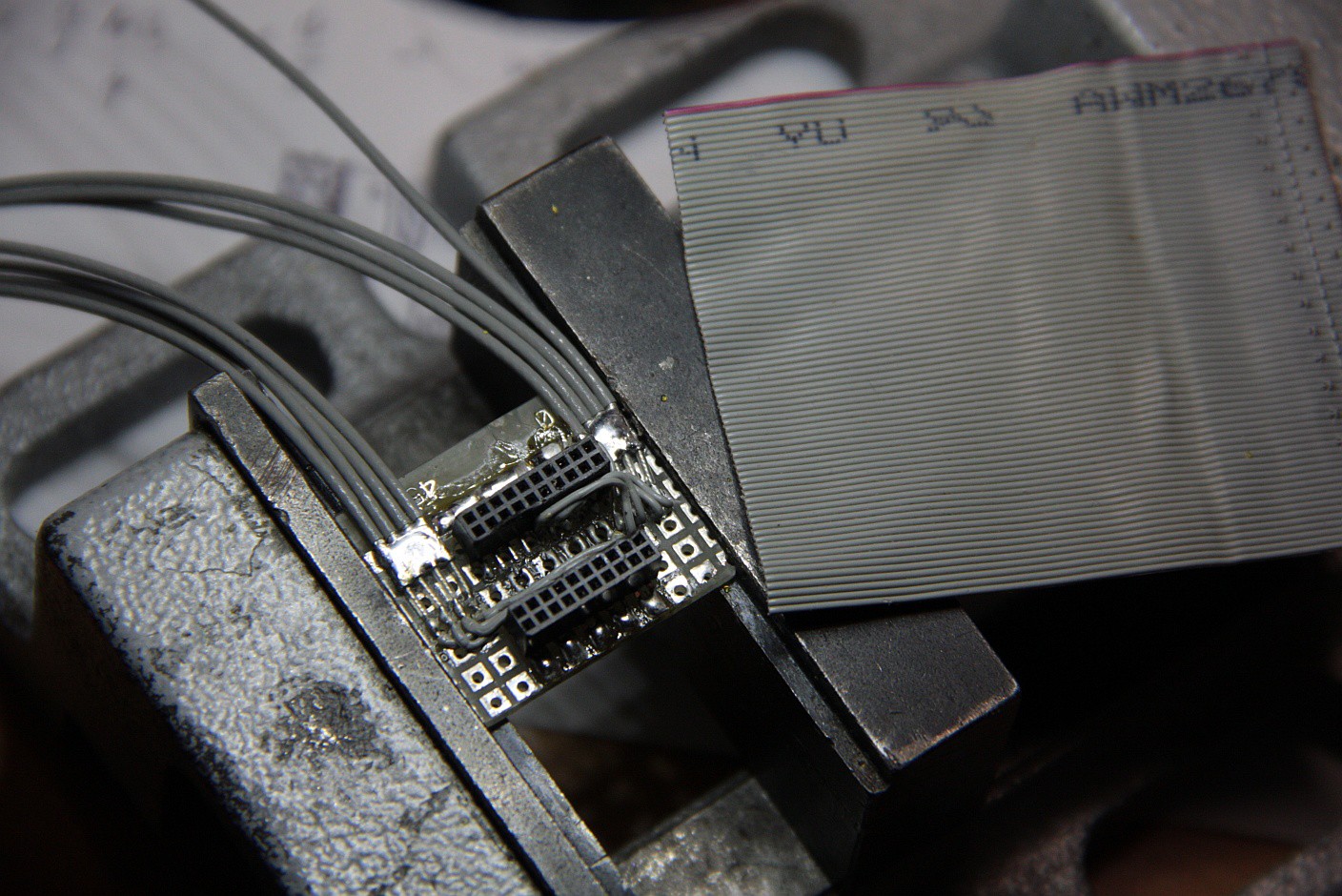
Here's the fun part: soldering the U.FL cables and attaching 0.635mm wires to route the connections to the diodes
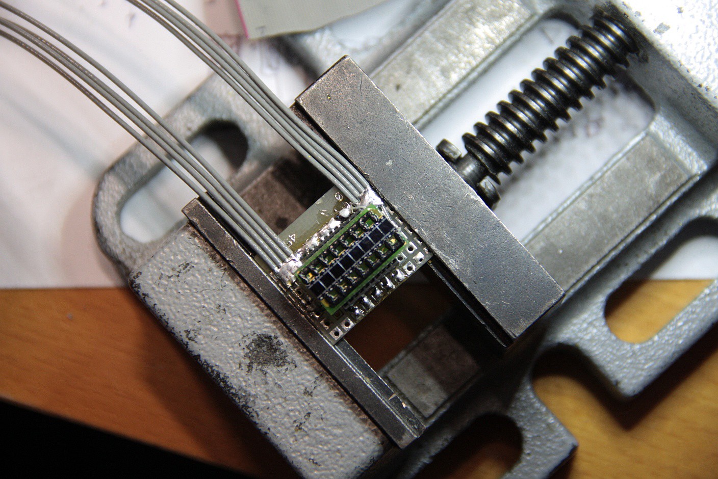
and it's done. Let's mount the PIN diode array (it's hard to see but there are 2 diodes on each of the 8 chips, 16 pixels in total, only the upper half is in use right now)
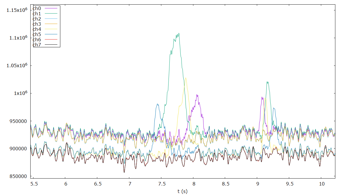
I haven't bothered to get the pinout right so the channels are out of order but you can convince yourself that
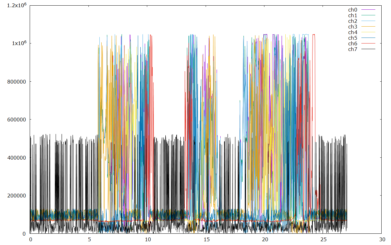
* all channels are working to spec
* no shorts
* gains are compatible
test setup: reset and acquire background for dimmed laptop monitor showing a black image with a 1px white line, move diode array across the screen, illuminating one pixel at a time as they pass. Note also that the zero line is noisy due to brightness fluctuations in the backlight an that the LCD is not completely dark, so some jaggedness is to be expected.
![]()
coming up next:
* electrically shielded housing, provisions for x-ray aperture
* systematically redo PCB mods for noise mitigation and quantify significance
* measure some stuff!
You may have noted that we're diverting a bit here. That's be cause the hardware developed here will be used in an x-ray backscatter imaging experiment. Apart from that we're still on track with the Optical Inch.
-
The Dark Side
01/08/2017 at 19:20 • 0 commentsthe DDC acquisition chips achieve 100% sampling time by alternating between two integration stages per channel identified by "Side A" and "Side B" for the two integration phases.
Now these integrators are not made equal, which causes different offsets and scaling factors to be applied to the acquisitions. I did find the offset issue somewhat disturbing so I addressed it first.
Let it also be noted that the CONV synchronous effect might also be in part due to LED activity or the CONV signal / trace itself. I remember it getting worse as the range is decreased.
Here we go:
![]()
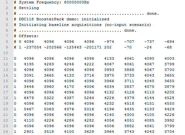
unfortunately the first four data channels (mapped to input channels 1, 3, 5, 7) have some issues. I've contacted Ti to see if they have an idea and can help me out.
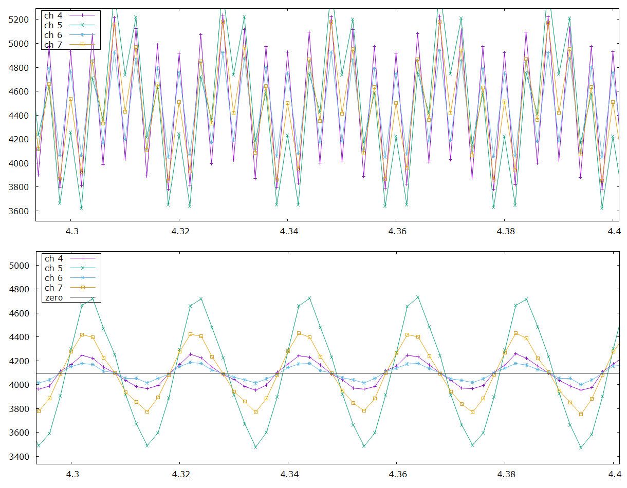
The remaining four channels however look quite promising, they still work quite well. For the DDC118 with 8 inputs there are 16 offsets to be kept track of. Here's what the output data looks like without (and below, with) Side A/B offset compensation:
![]()
this is 500 samples/sec, 350pC full scale and the board has just a bunch of 20cm long coaxial cables attached to the inputs.
I've also created a github repository and uploaded the demo code.
-
InGaN LEDs as photodiodes!
01/02/2017 at 21:14 • 0 commentsObservations (yay!):
1. 50 Hz noise still can easily couple into the system
2. LEDs with a larger bandgap (for 400nm, off by 0.3eV) can still detect some 450nm light from white LEDs
3. there's other noise present, possibly because of the USB 5.0V power, microcontroller and UART activity - and it's correlated among the channels
200 samples/sec, 200 pC range:
plot for [i=2:9]'20170102-16 capture20.txt' u ($0/200):i smooth kdensity bandwidth 0.01 t sprintf("ch%d",i-2)
![]()
-
PCB clean-up and endianness
01/02/2017 at 16:38 • 0 commentsAlright, this project definitely got some love today. That PCB is really not that great (as in: damn that DDC118 is super sensitive).
Changes (3 years in the making ^^):
![]()
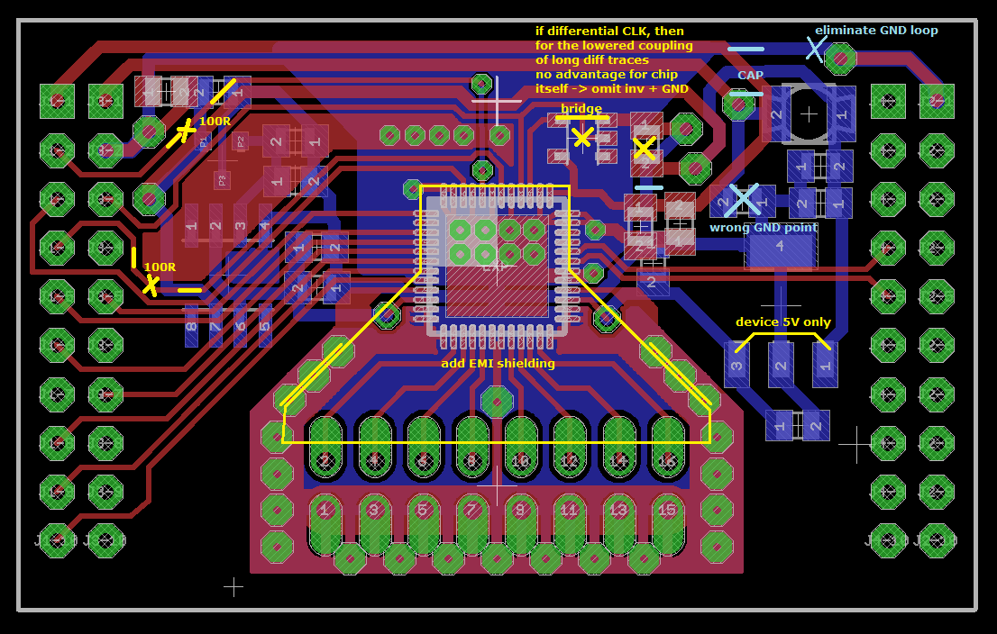
- add missing bypass caps, mostly 220nF ones, test direct bypass to AGND polygon (no significant change from the latter)
- insert 100R clock termination resistors for T2CCP1 (@2.5 MHz) and DCLK (@10 MHz)
- insert 22R in the trace supplying the voltage reference -> no significant change (not shown in layout changes)
- insert 10k series resistance on REF3040 output -> no significant change (not shown in layout changes)
- omit 74AHC1G14 single schmitt inverter. I had re-routed the cap next to it for proper 3.3V bypass including 10R resistor to the caps below but no improvement was evident. A differential clock source only really shines on larger PCBs and flex cables.
- see that cap between the second trace on the top and the LDO tab pad where it says "wrong GND point"? That cap was moved upwards because connecting it to the bypass caps behind the filter would only couple noise from the input to the output. The two traces on the top right are static and don't couple much noise into the rails.
- add EMI shielding (tin coated sheet metal cut to size) above the chip and sensitive traces. That did away with a good fraction of the 50 Hz line perturbations which are superbly evident at 100 samples/sec. The A (B) side samples themselves are supposed to be rather consistent but showed slow beating without the shield. Additionally the noise introduced by an approaching hand is mostly gone without anything connected to the inputs.
Code changes:
- endianness issue resolved, both 16 bit and 20bit modes look good
- right now both integrator sides are being printed, looking good at 400 samples/sec but that might get worse as integration time is increased due to differences in the capacitances and active analog front end circuitry
- SPI speed changed to 10 MHz
![]()
Next: There's a hint regarding noise performance. For best performance the CONV transition needs to happen within +/-10ns around a T2CCP1 rising edge. Right now CONV is generated from within an ISR which has delay and jitter.
This may possibly be solved by routing a trace from a T1CCPx pin to CONV and subsequent configuration of both timers. All timers have pre-scalers and can be synchronized to some extent. Not sure what cases can crop up though. Maybe It's best to latch CONV with T2CCP1 and keep the interrupt based scheme.
NC7SZ175P6X looks right for the job.
In summary, ditching the schmitt inverter for !DCLK (which likely inejcted more noise than help reject transients) and adding the E field shielding did a lot to improve performance whereas it is hard to tell apart what that course of ground re-routing and bypassing actually did. Maybe it wasn't that big a deal to begin with. Powering the Launchpad + DDC118 externally and testing it with floating pot. laptop showed no difference.
-
Hello World
01/01/2017 at 14:11 • 0 commentsI've finally managed to sit down and write a few lines of code to make our old friend the DDC118 work. The main bug in the PCB design is that the analog supply voltage was designed to run at 3.3V (where it should have been 5.0V). The direct connection to the USB 5V in conjunction with some other effects appear to cause some minor noise issues.
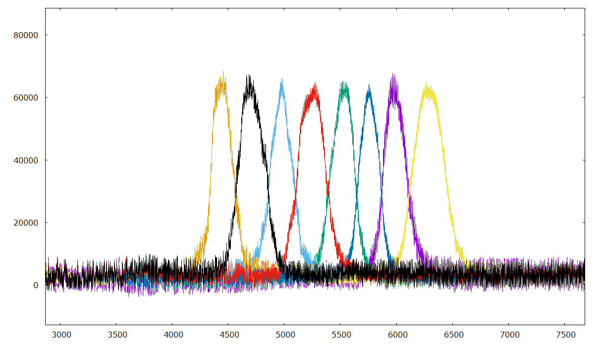
Below I'd like to share the colorful plot of my finger swiping across the exposed input pads in a / \ / pattern. Sorta works. Now for some clean-up...
I've added the demo code to the project. The DDC interface is pretty straight forward, I'll have to give the byte chunk paritioning a good look though.
![]()
As you may tell there's a problem with the byte ordering. This is fixed later (endianness).
-
DDC118 eval board
02/03/2016 at 16:00 • 0 commentsThis project is currently on hold. However I'd like to show you the DDC118 booster pack I designed to evaluate the current sensing ADC and have an ideal platform to test and characterize the photodiodes.
The Optical Inch
An approach to entry-level wideband spectrometry (color temperature & CRI, UV-A /UV-B dosimetry, material identification, ...)
 helge
helge