Hiroyuki OYAMA
-
New VA Engine: 3 Oscillators + Noise → TPT/ZDF Ladder Filter
8 hours ago • 0 commentsI’m continuing to explore the software side of this project and revisiting the overall signal chain. I realized that, like many classic synthesizers, mixing multiple oscillators first and then shaping the combined sound with a single filter is simply easier to work with.
So I reworked my synth’s signal path and replaced the engine with a more traditional VA structure: three oscillators + noise feeding a single ladder filter.
In parallel, I’ve been working on a TPT/ZDF ladder filter. It’s computationally expensive, but the result is worth it—the filter sounds great, stays stable at high resonance, and handles aggressive parameter changes smoothly.
-
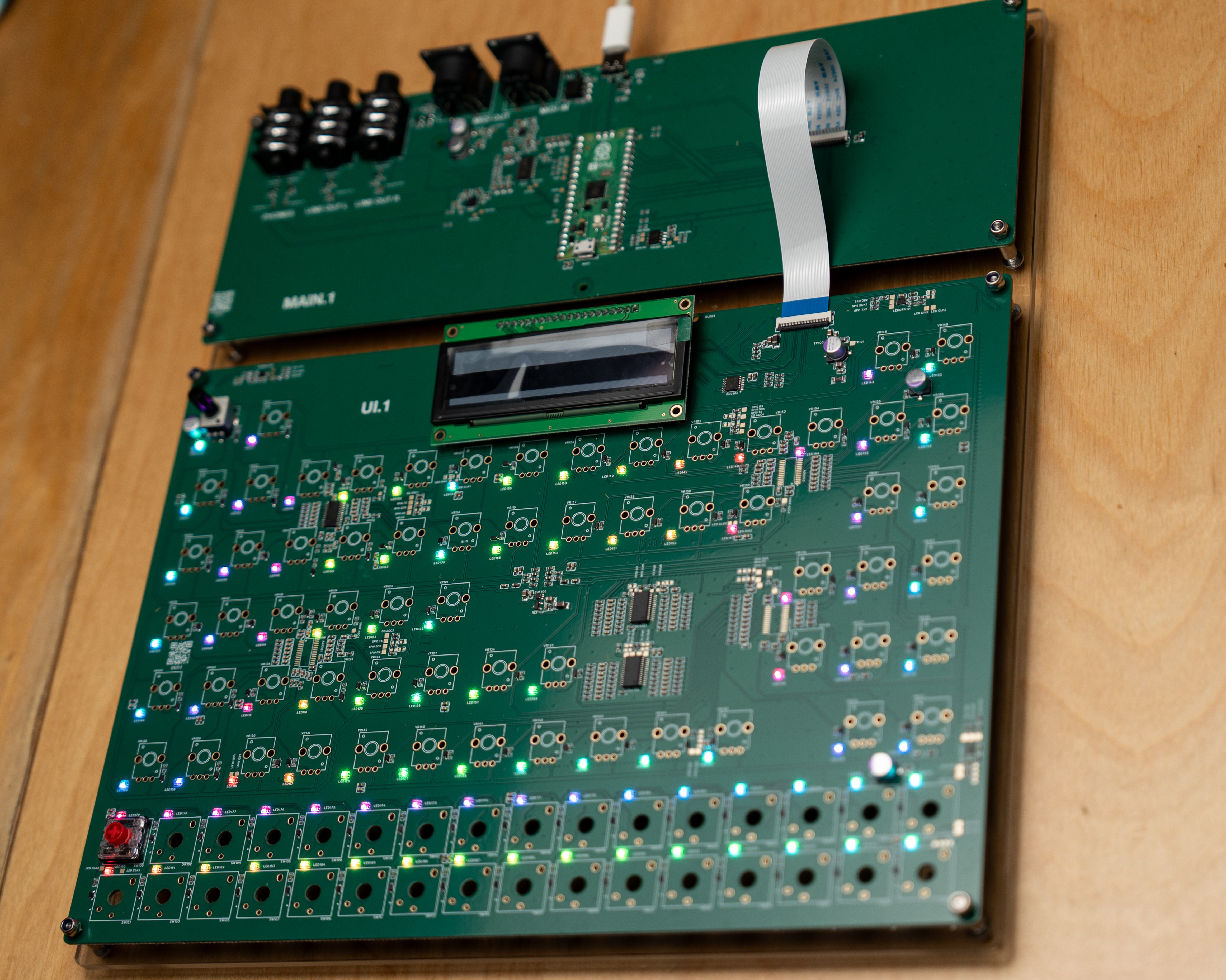
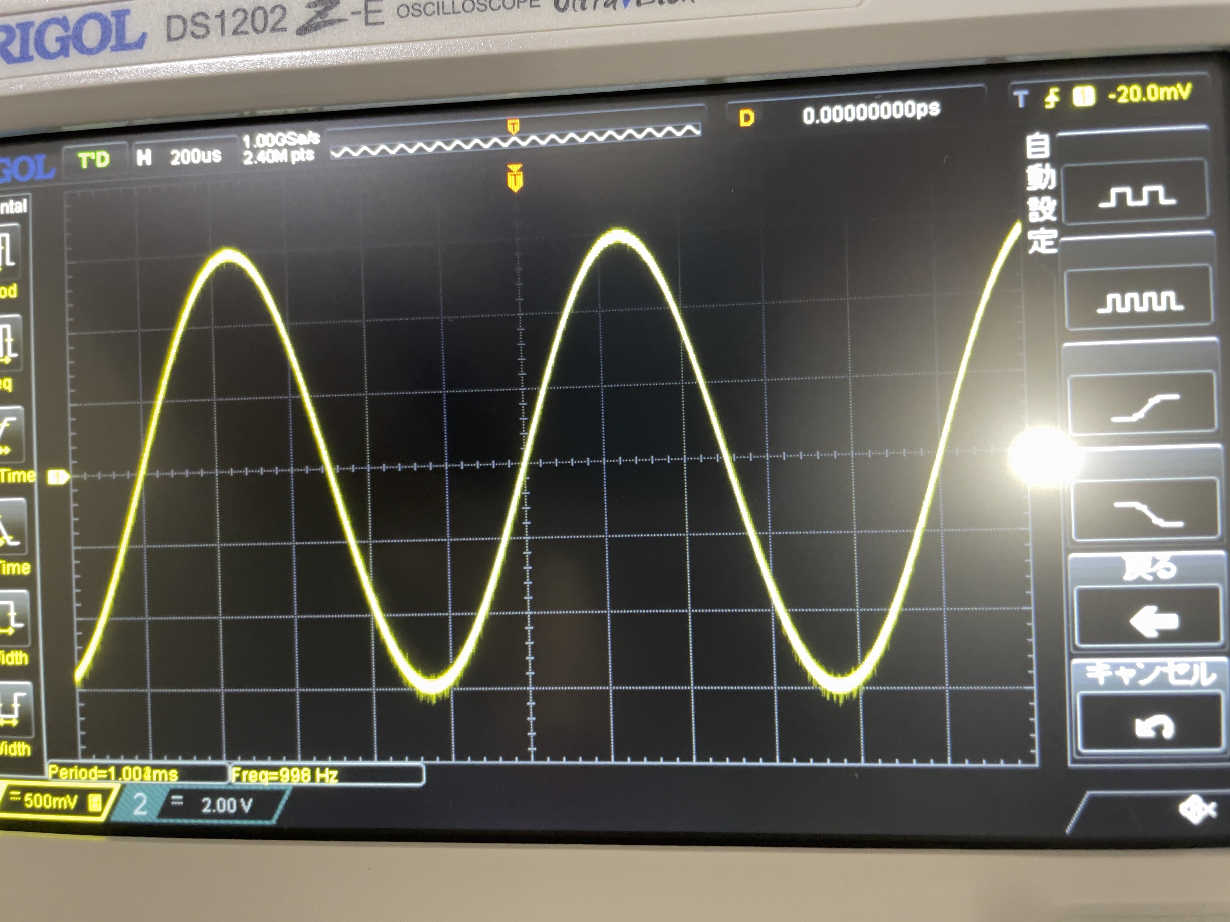
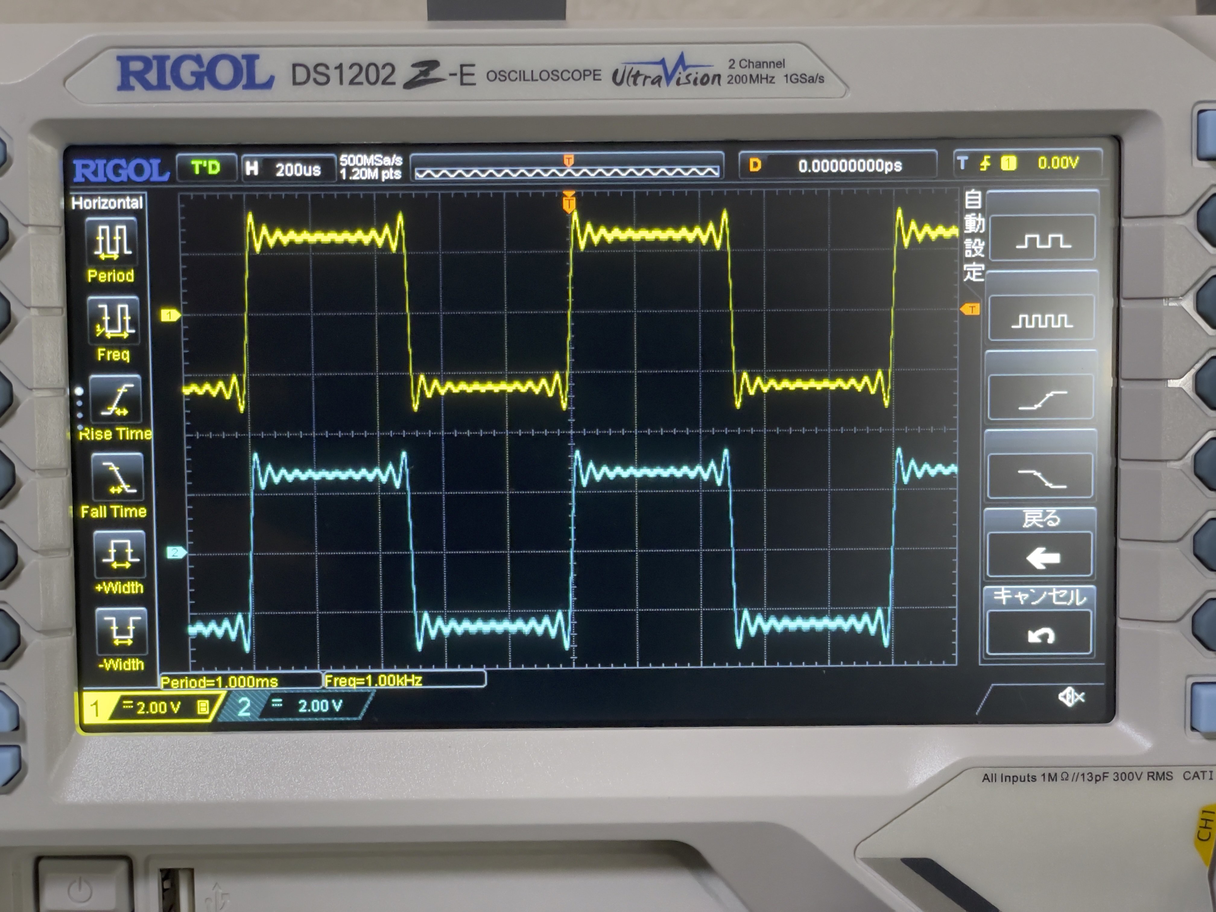
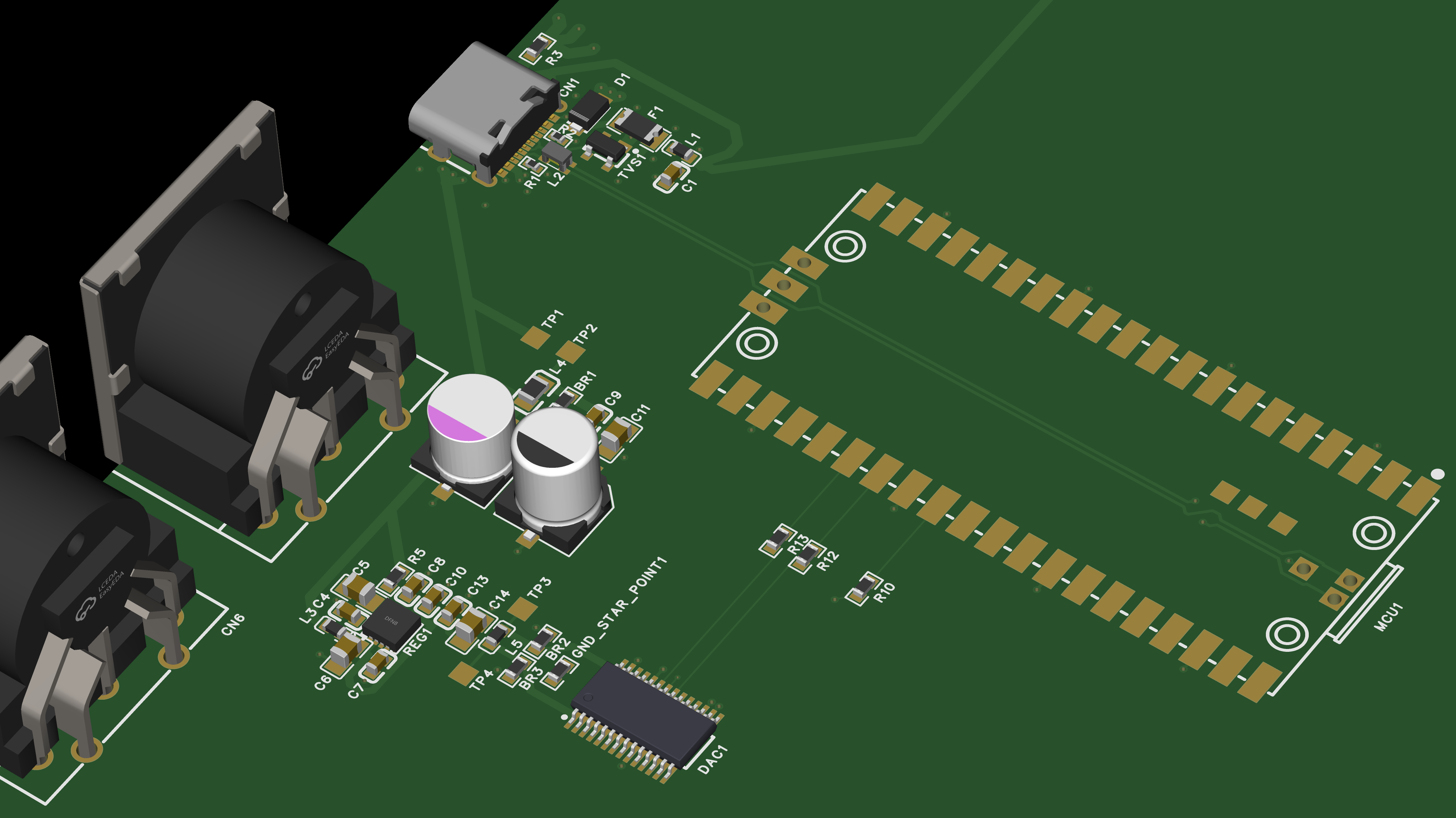
First PCBs Arrived and Fully Tested
11/28/2025 at 04:36 • 0 comments![]()
After a long pause, here’s an update on the hardware progress.
I’ve received the first batch of PCB/PCBA and finished testing all the major components on the board.
To my relief, every subsystem — the ADC/knob matrix, LED chain, OLED display, FRAM, and I/O expanders — is working exactly as intended.
One of my biggest concerns was ADC noise, but in practice it appears to be within a very comfortable range, so that was a nice surprise.
![]()
![]()
There was one minor issue: the audio output noise floor is a bit higher than I expected. It’s not severe, but I’d like to improve it in the next hardware iteration.
For the DAC path, I ended up writing a custom I²S Standard 24-bit PCM DMA streamer for the PCM5122.
Originally I planned to integrate this into the pico_audio library, but that approach required too much overhead, so I opted for a lightweight, dedicated implementation.
For a quick sound check, I generated a simple saw wave on six instances, tuned them slightly apart, and stacked them into a unison tone. Nothing fancy yet, but it’s a solid first sound coming from this board.
More updates to come as I move into the next iteration.
-
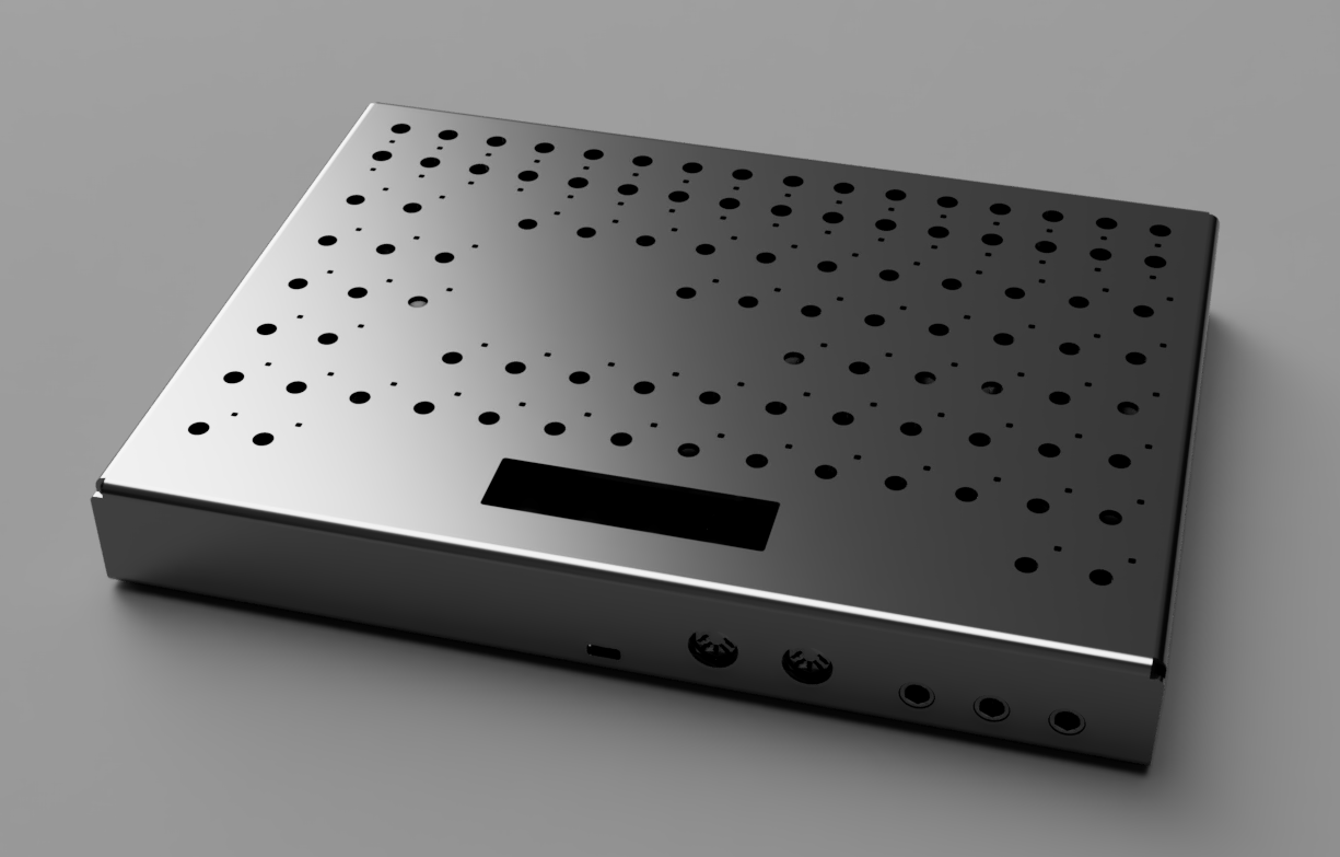
First enclosure render
11/15/2025 at 16:39 • 0 comments![]()
I’ve been working on the sheet-metal enclosure for Darśana.
This is my first proper attempt at modeling the case in Autodesk Fusion, and it took me much longer than expected.
Even something as simple as “a box with holes” turned out to involve lots of details—sheet-metal rules, bends, corner seams, offsets, and so on.
After many trial-and-error cycles, I finally managed to produce a rough top-panel render that includes all the openings:
potentiometers, keys, the OLED window, and the rear connectors.
It’s still very much a draft, and I’m sure I’ll revise most of it once I start checking clearances and mechanical tolerances.
But for now, I’m just relieved that the basic shape is in place.
More refinements will follow as I get more comfortable with Fusion.
-
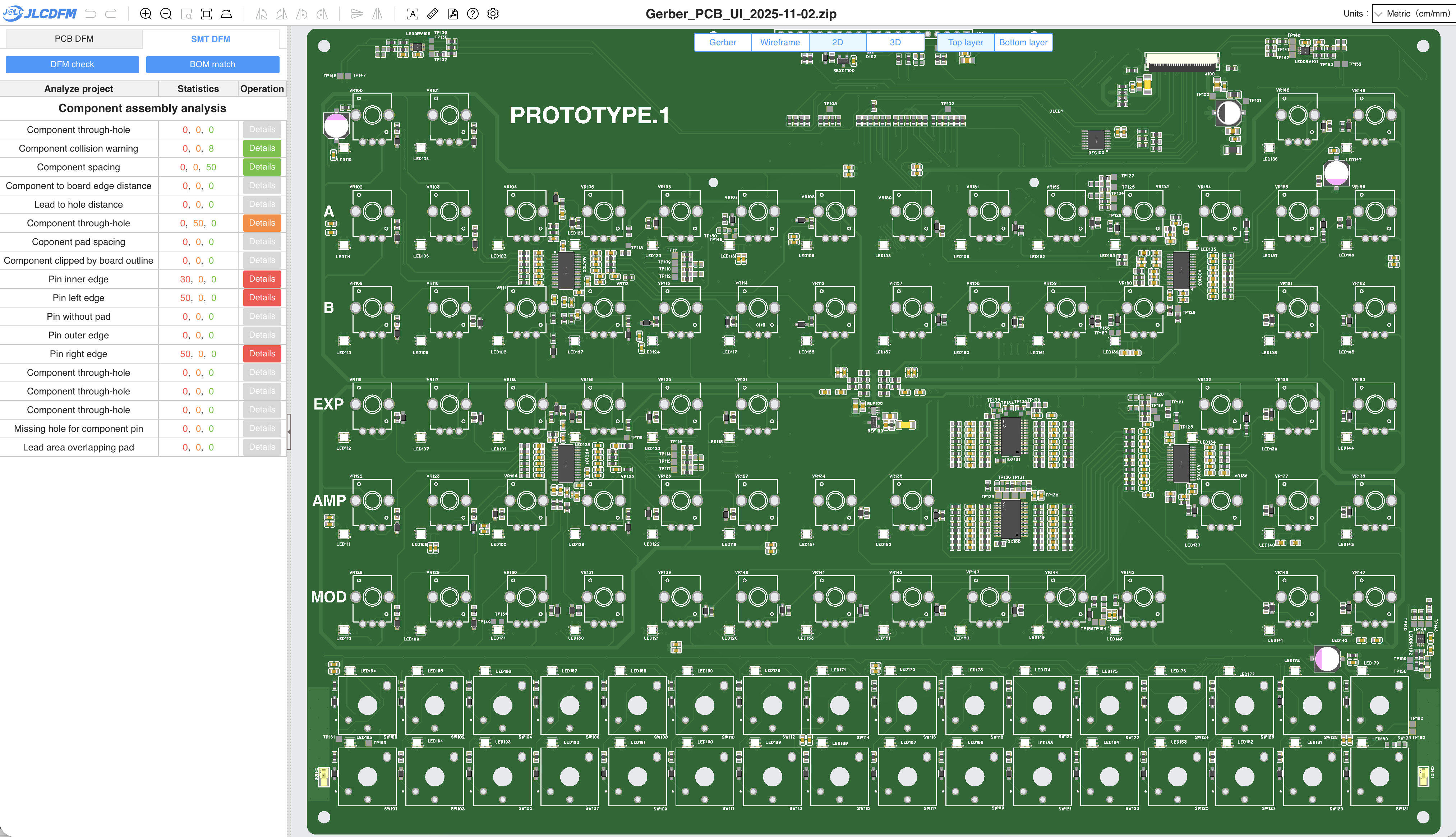
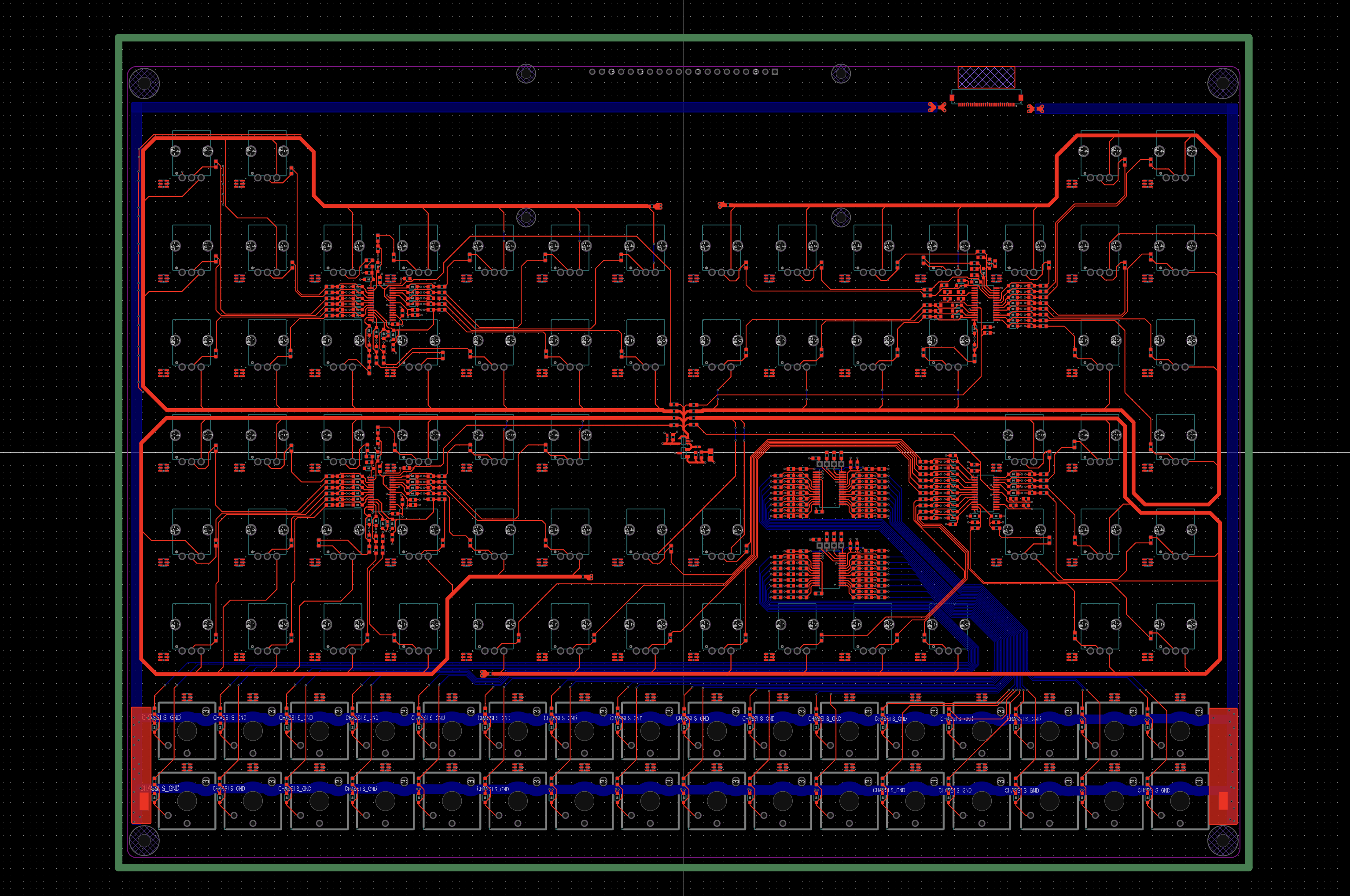
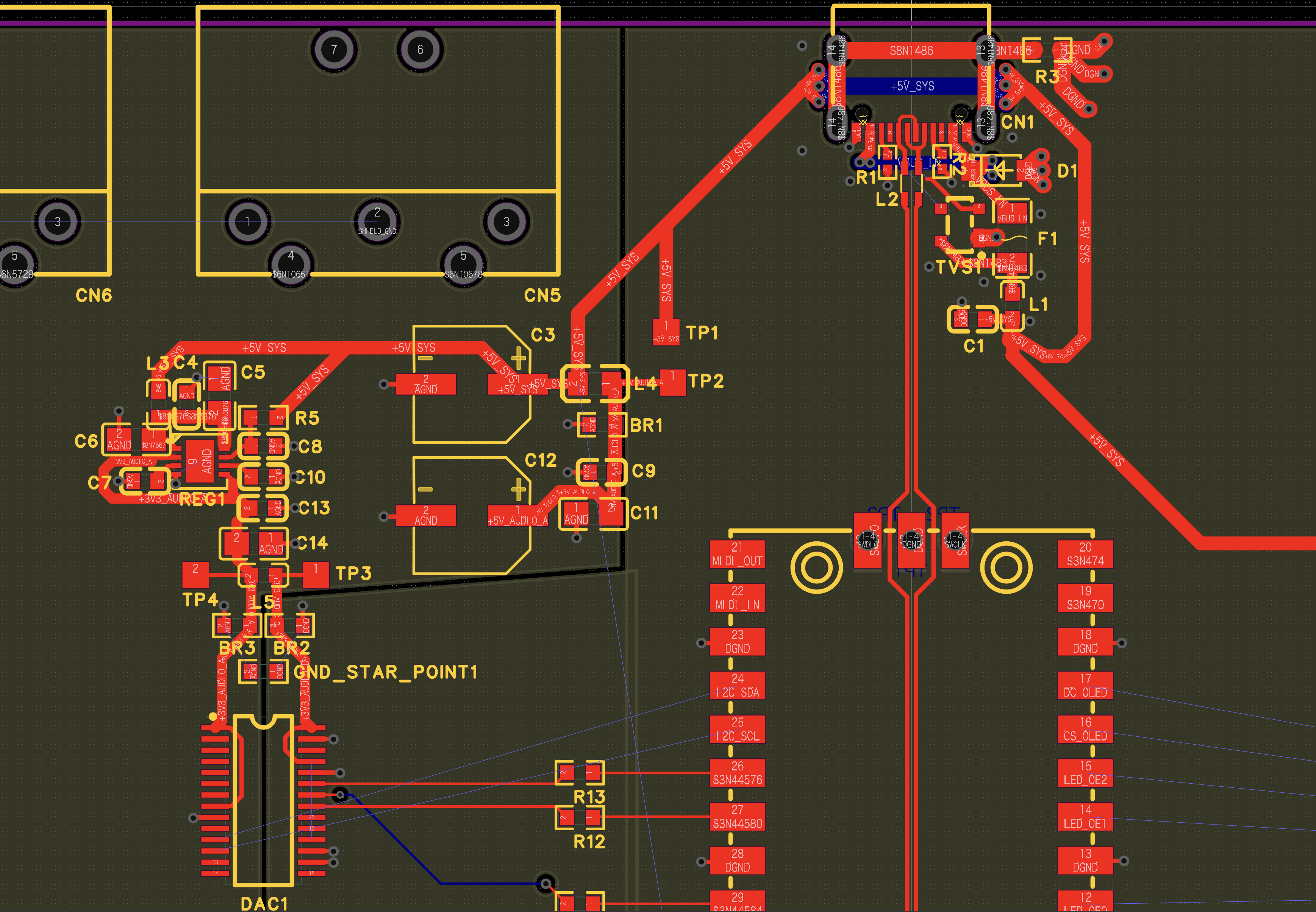
Survived the DFM gauntlet
11/01/2025 at 16:49 • 0 comments![]()
I ran exhaustive checks using JLCPCB’s online DFM tool and revised the design until it was fully manufacturable for both PCB and SMT assembly.
Some traces were redrawn to flow more naturally, some issues were patched or adjusted with minor compromises, and a few alignments had to be intentionally broken to make things fit.
All major risk points (Dangers) have been cleared, and the remaining Warnings are within acceptable limits for production.
After going through this process, the overall routing feels cleaner, and the entire circuit design now looks more coherent and balanced.
-
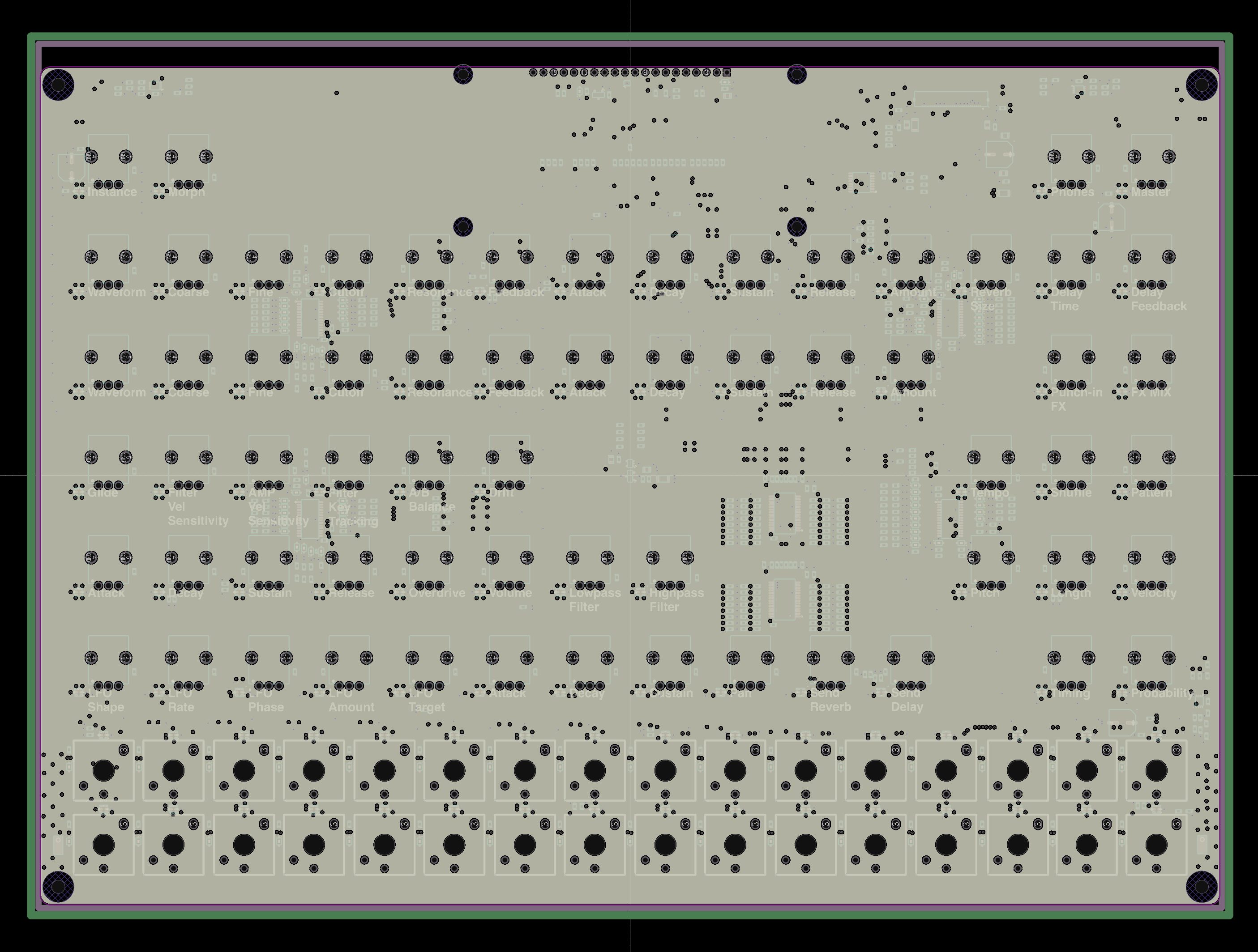
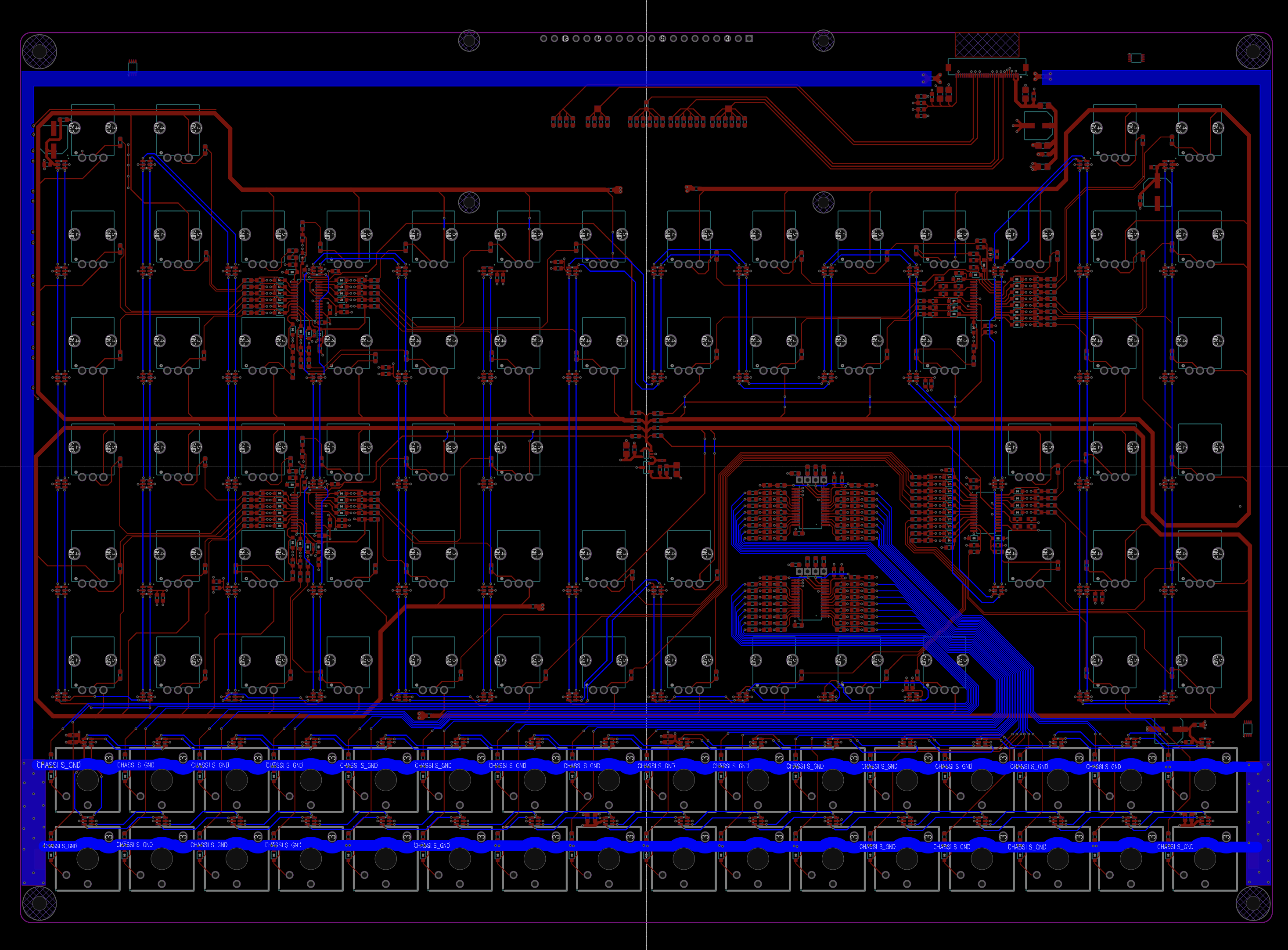
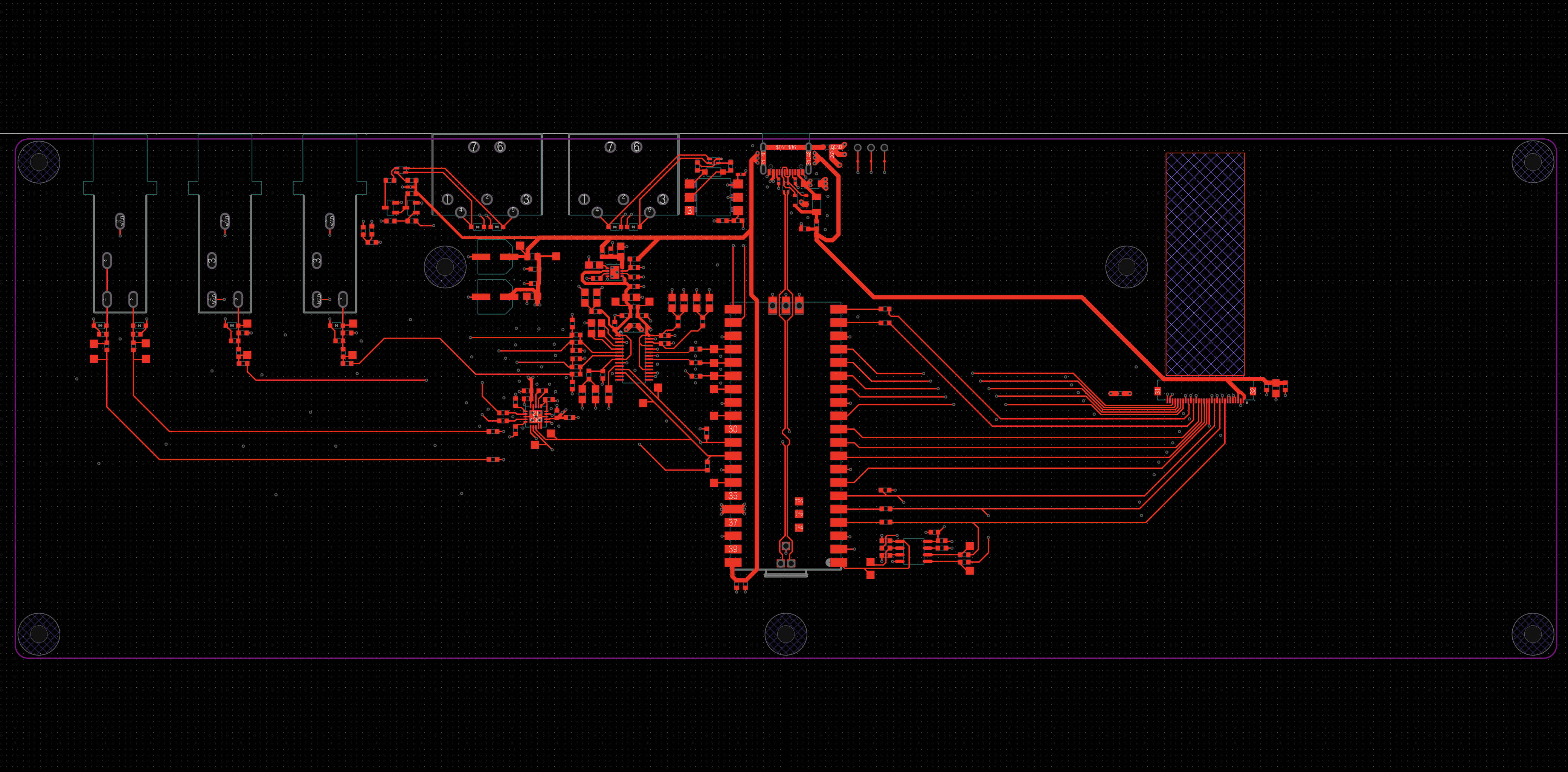
All Components Placed, Routed, and DRC Cleared
10/29/2025 at 15:52 • 0 comments![]()
The UI board is now fully routed — every component has been placed, all nets connected, and the design passes DRC with no errors.
This was by far the most complex part of the Darśana hardware: 64 potentiometers, 32 key switches, 96 LEDs, four ADCs, two IO expanders, OLED, and all the SPI buses packed into a 4-layer board.
Careful power segmentation paid off:- +3V3_UI and +3V3_UI_A rails separated and thickened to 1 mm
- +5V_SYS → +5V_UI_LED isolated via 100 mΩ resistor
- VREF and ADC lines shielded with GND guards
- IOX inputs protected by RC (150 Ω + 1 nF) and 10 k pull-ups
After endless nights of routing and revising, the DRC finally came back clean.
Next step: a slow, quiet design review — then it’s time to generate Gerbers and send the first UI board to fabrication.
![]()
![]()
![]()
![]()
-
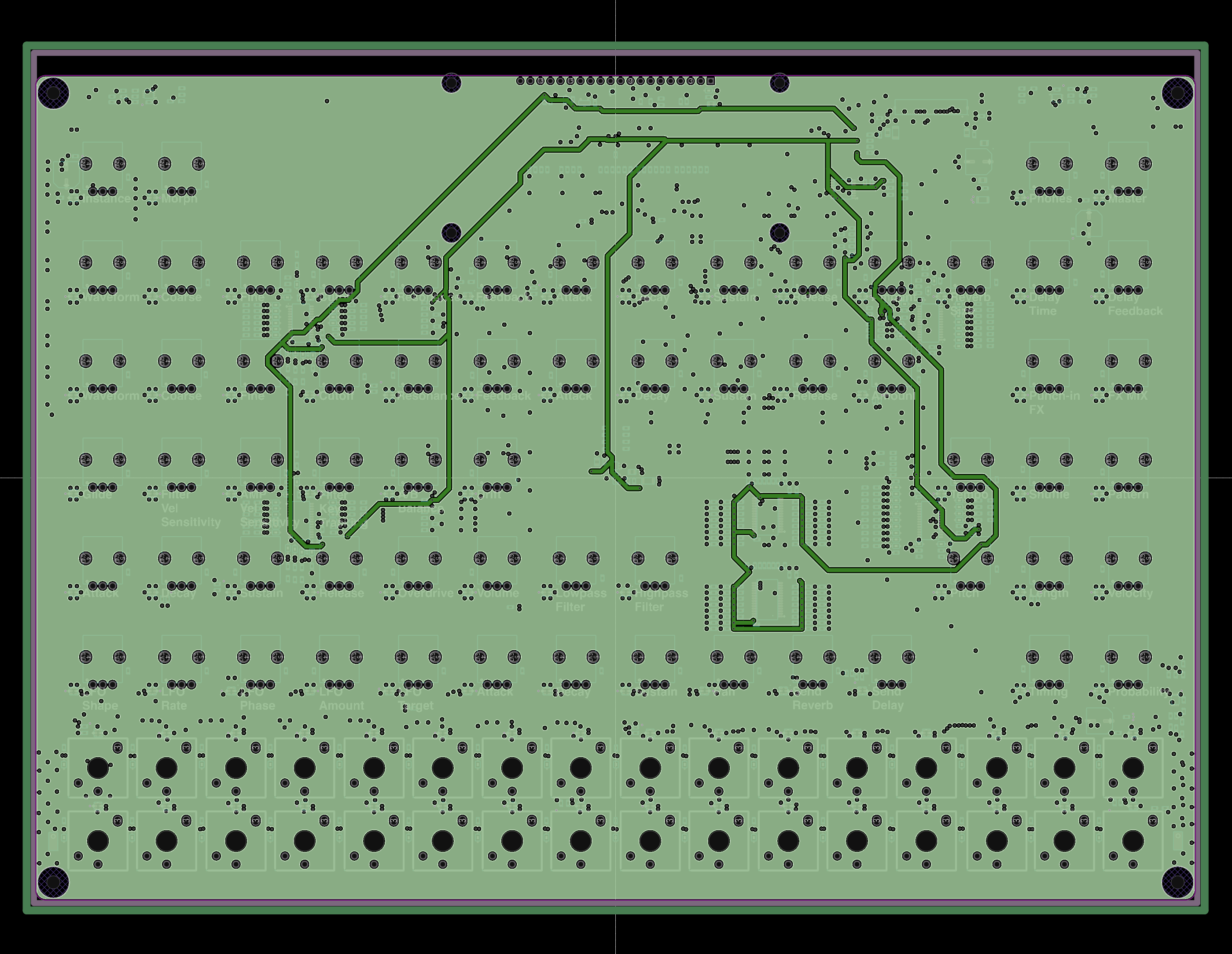
UI Board LED Routing Complete
10/27/2025 at 14:10 • 0 comments![]()
Today I completed routing all 96 LEDs on the Darśana UI board, including those for the key switches.
The southern “dead-end” section turned out to be the biggest challenge, but all LED chains are now fully connected. With this, all display-related circuits — LEDs and OLED — are now wired and ready for verification.
To prevent interference with the analog input section (ADC / VREF), the LED layout follows a layered structure:- LED signal lines are routed on the bottom layer,
- Analog VREF and potentiometer wiper lines remain on the top layer,
- and a continuous L2 GND plane is placed between them to minimize coupling.
This approach allowed me to arrange 64 potentiometers, 32 key switches, and 96 LEDs in a high-density layout while keeping the overall circuit structure well organized.
The next steps will be:- placing LED drivers at the origins of each LED chain,
- completing the SPI routing (SCK / TX / RX / CS), and
- refining the inner2 power plane for +3V3_UI_D, +3V3_UI_A, and +5V_UI_LED.
Now, every visual element on the UI board finally has a clear path for light to travel.
-
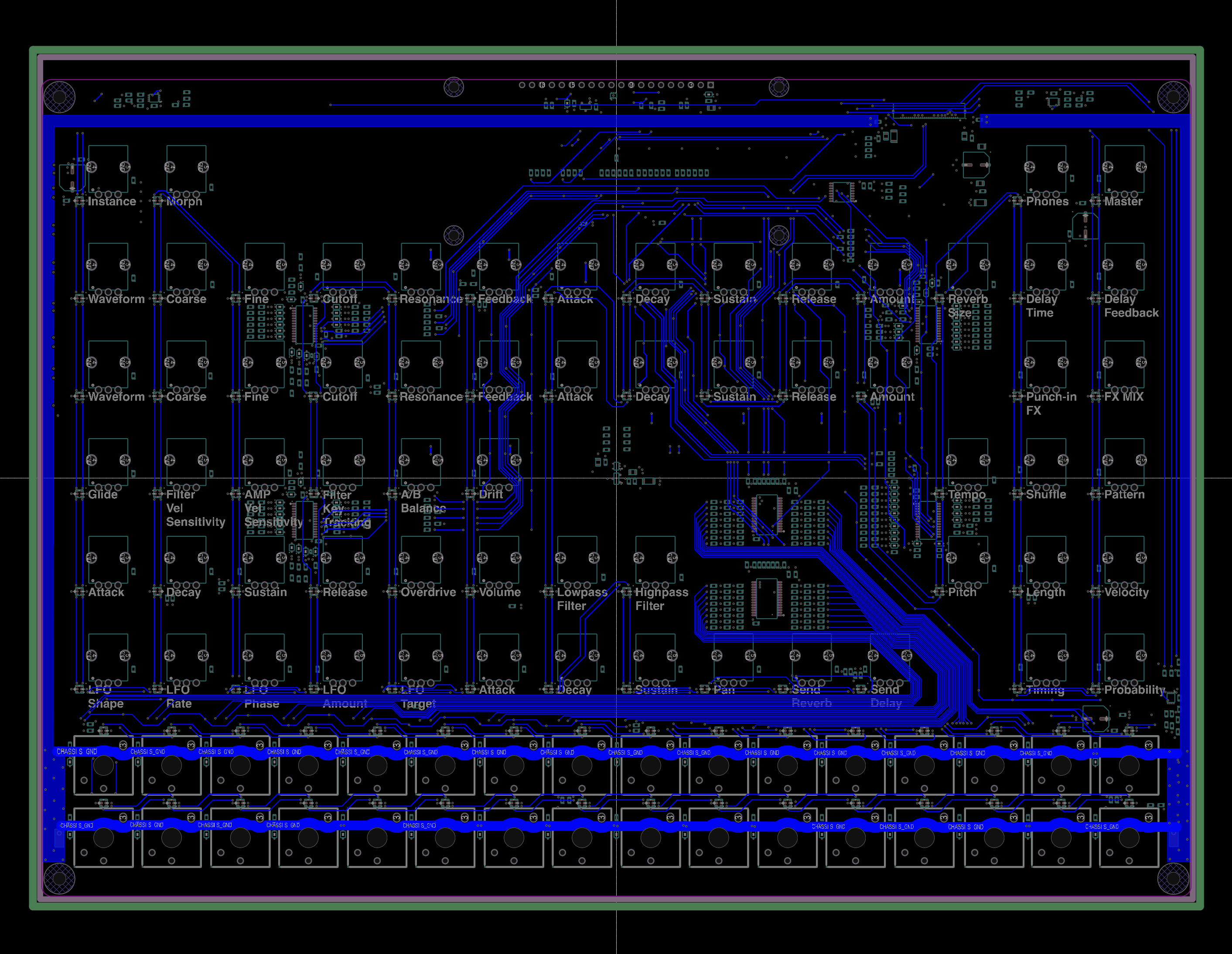
Input System Wiring Complete
10/26/2025 at 14:58 • 0 comments![]()
The UI board has finally passed its steepest mountain —
all potentiometer, ADC, key switch, and I/O expander connections are now fully routed.
This section was particularly challenging:
- 64 analog potentiometers (each with low-pass and reference routing)
- 32 independent key inputs through two MCP23S17 expanders
- Integrated ESD paths, shielding traces, and shared ground planes
- 96 LEDs to coexist in the same grid
After many iterations, I managed to fit everything while preserving:
- Continuous ground on inner layer (L2)
- Reserved space for LED horizontal buses (Bottom layer)
Next, I’ll start routing LED data and power (L3) —
but with the entire input system already verified, I feel the design has crossed its biggest hurdle. -
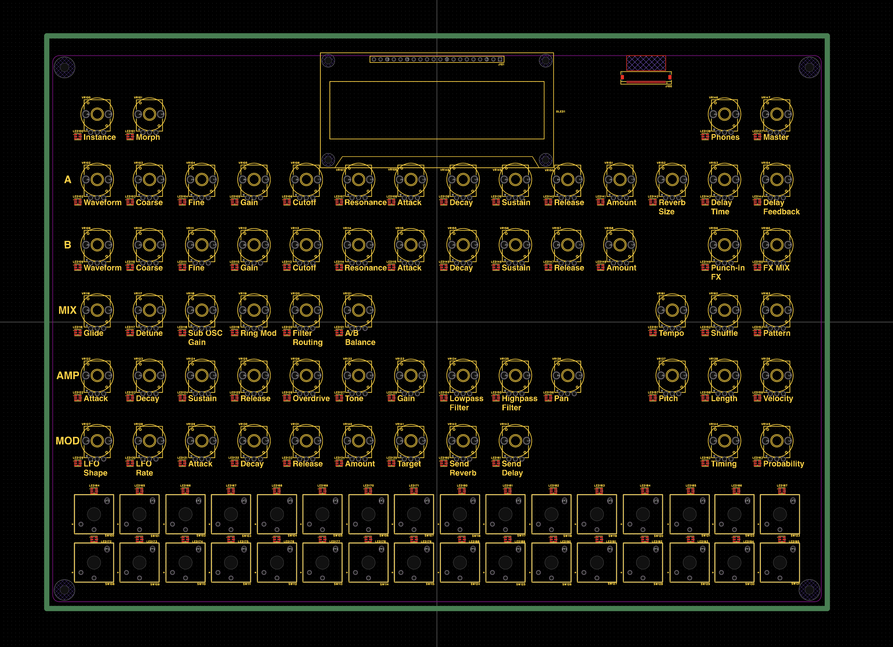
Where Analog and Digital Share the Same Dance Floor
10/21/2025 at 14:51 • 0 comments![]()
Exploring the physical limits of Darśana's UI board.
Placing every component directly on the PCB to search for the balance between ergonomics, circuit constrains, and visual rhythm.
64 potentiometers, 32 key switches, and 96 LEDs - all living toghether on a single mixed-signal board.The challenge is not only routing signals, but also shaping the flow of analog and digital currents without splitting grounds.
This is where engineering and composition meet: how to make every path quiet, logical, and beautiful at the same time.
-
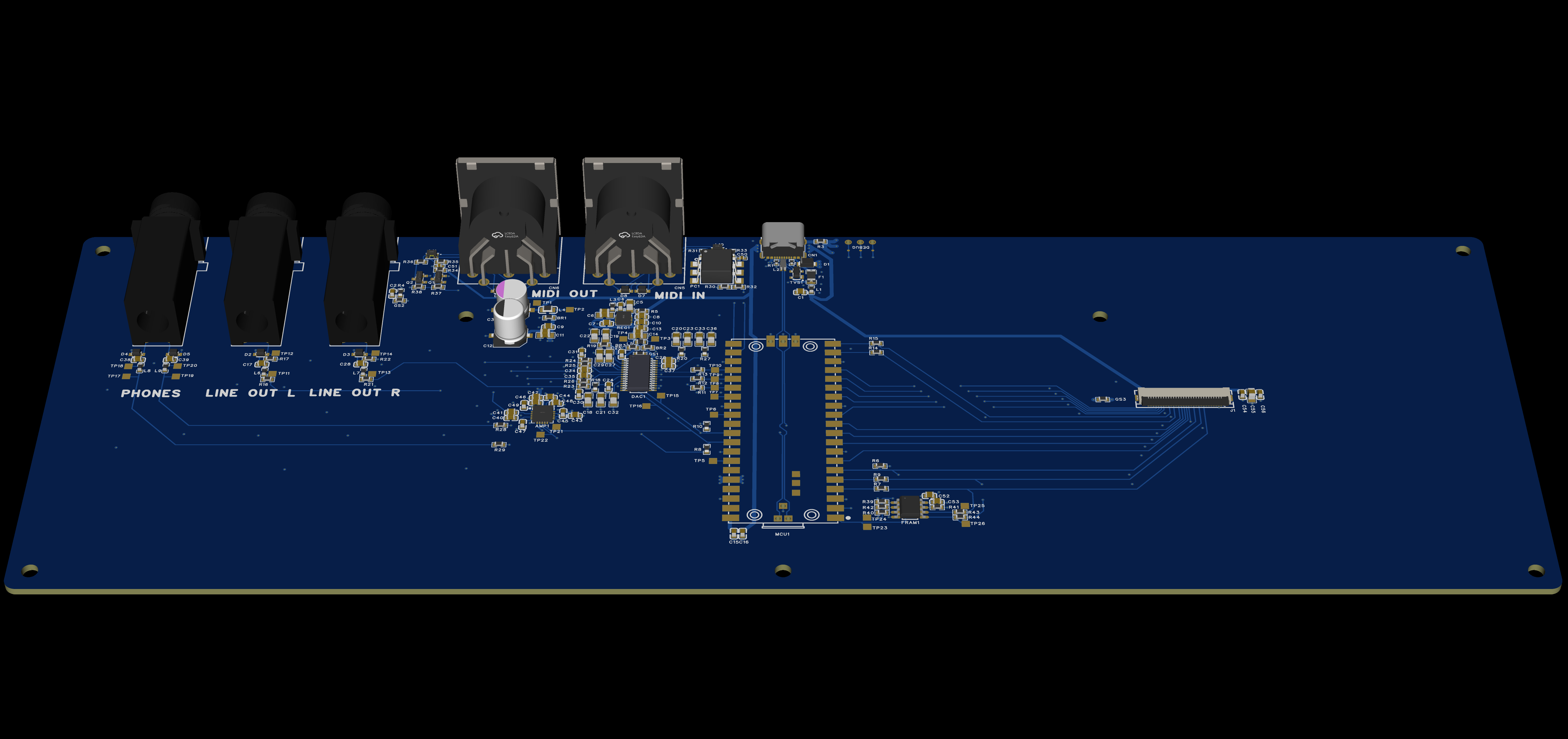
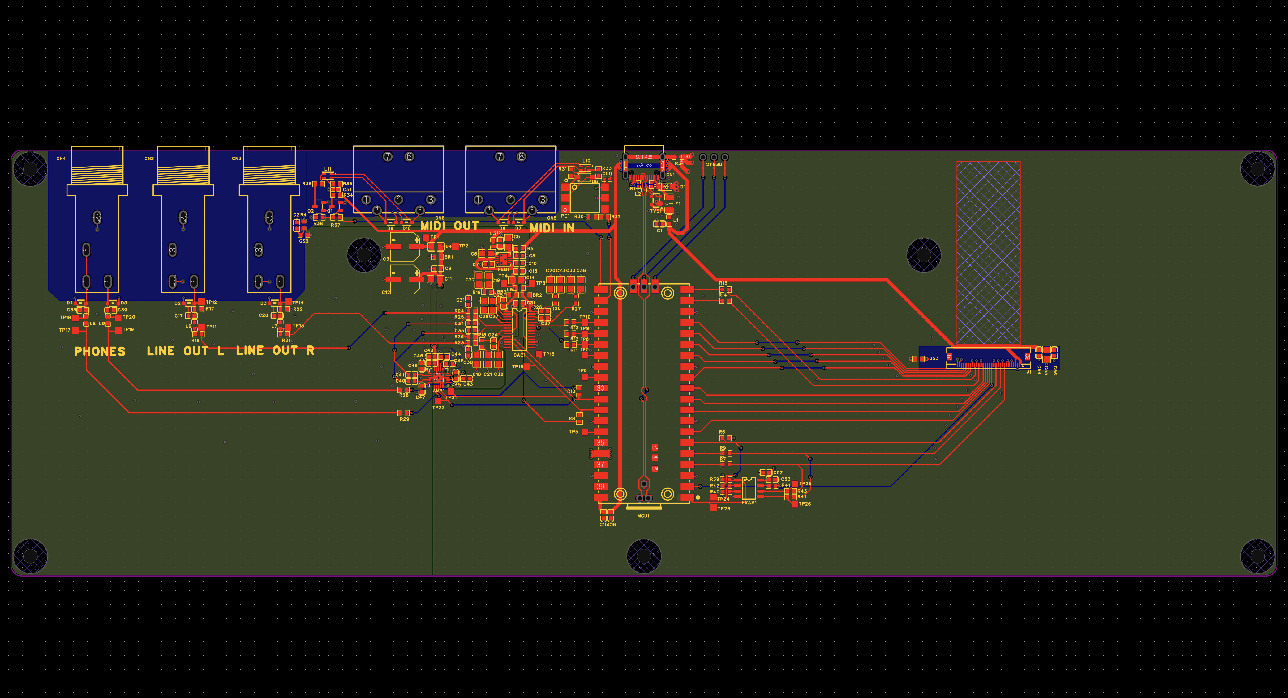
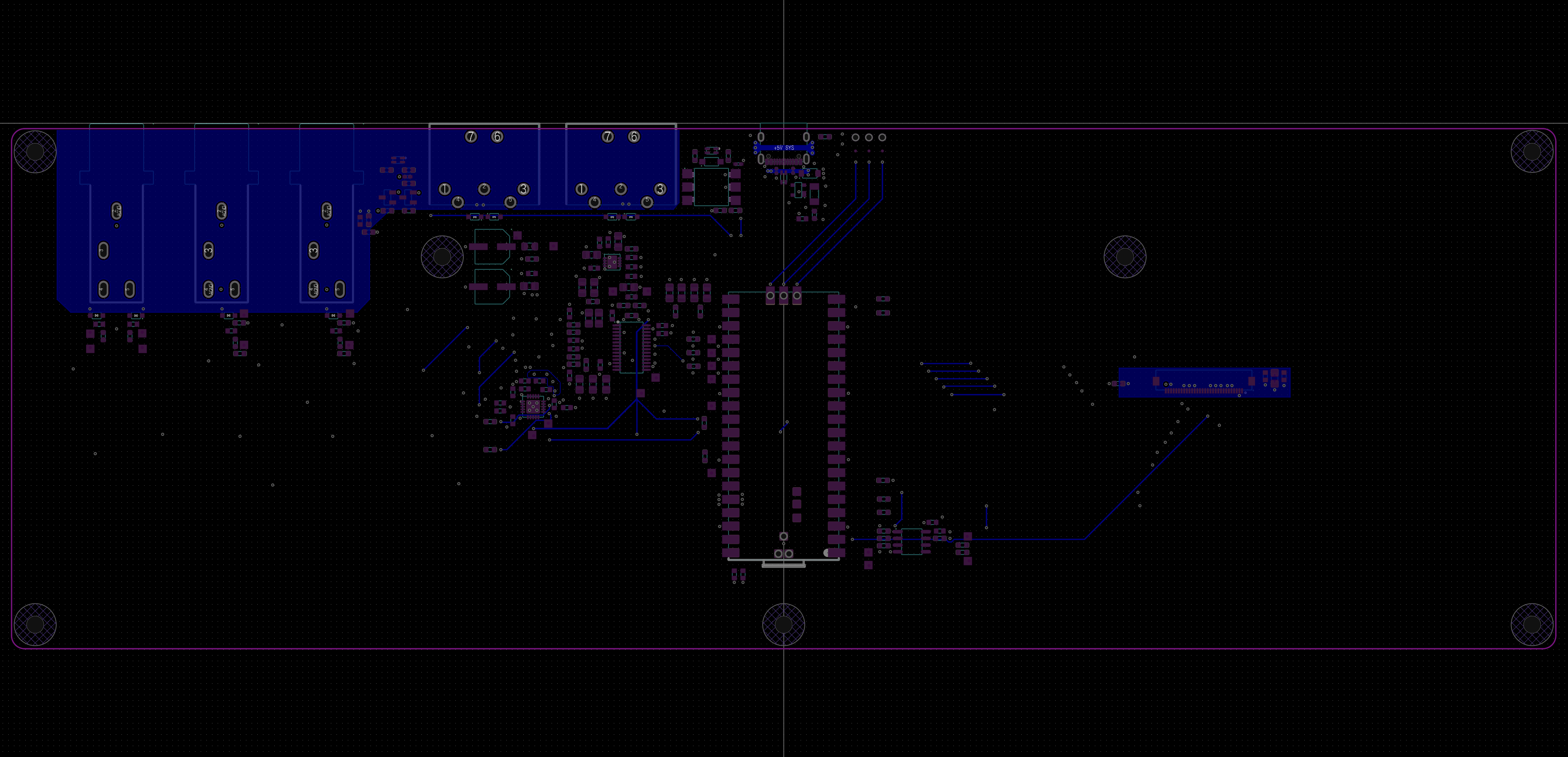
Main Board Layout Nearing Completion
10/18/2025 at 18:20 • 0 comments![]()
The main board of Darśana is almost complete.
This revision focuses on refining the audio power and signal layout, separating AGND/DGND domains, and finalizing the analog output paths (DAC → Line / Phones).
- Introduced a local `+5V_AUDIO_Analog` plane on Inner2 exclusively for the headphone amp (TPA6130A2).
- This simplified routing and reduced coupling around the charge pump region.
- Maintained at least 2mm clearance between the charge pump loop (CAPP/CAPM/VNEG) and all power traces.
- Ensured continuous AGND on Inner1, no necks or splits.
With all components placed and DRC passing cleanly, the PCB measures 294 × 99 mm — fitting perfectly inside the planned 296.6 mm internal width enclosure.
![]()
![]()
![]()
![]()
![]()
It was a demanding phase, but the layout came together faster than I expected — a relief, honestly. There are still rough edges to refine, and I can already see places that could be improved with more polish. Fortunately, there’s no rush. I’ll take as much time as needed to make it right.
-
Layout work has begun
10/15/2025 at 16:07 • 0 commentsI’ve only ever designed small, simple PCBs before, so this is a completely different scale—and I’m often unsure what I’m doing. Still, with the help of my LLM assistant and all the advice buried in forum archives, I’m somehow managing to keep going.
- Decided the placement of the main connectors, the Pico, and the 30-pin FFC board-to-board connector
- Fought through the maze around the USB Type-C connector footprint
- Routed USB D+/D- to the Pico 2
- Placed the DAC / AMP power supplies
- Connected the I2S lines for the DAC
To make these routes flow more naturally, I completely reorganized the Pico pin map, arranging it so that the UI bus(SPI0, SPI1) comes out on the right side and the DAC/AMP bus(I2S, I2C) on the left—much cleaner now.
Still feels like it’s never going to end.
![]()
![]()
64-Knob Virtual-Analog Synth on Pico 2
A 64-knob virtual-analog synthesizer on Raspberry Pi Pico 2 — fully tactile, no menus, real-time control.