trashtronic
-
Data capture
10/20/2025 at 13:35 • 0 commentsFor digitalisation purposes i wrote little C program for STM32F303. I had devboard with this IC laying aroung and it incorporates impressive set of analog functions so it was no-brainer. This program oversamples ADC input to get higher resolution data and streams filtered data through USB-CDC interface which is interpreted by serialplot. Here is live video which shows that it is not a fluke - mechanical stress indeed influences substantially voltage offset!
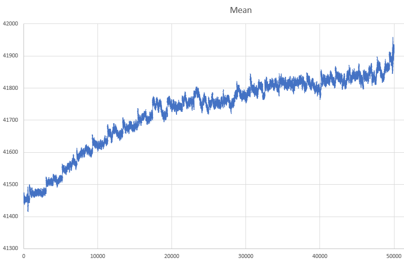
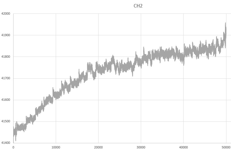
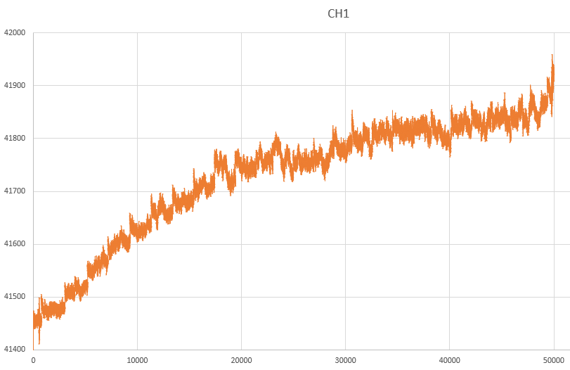
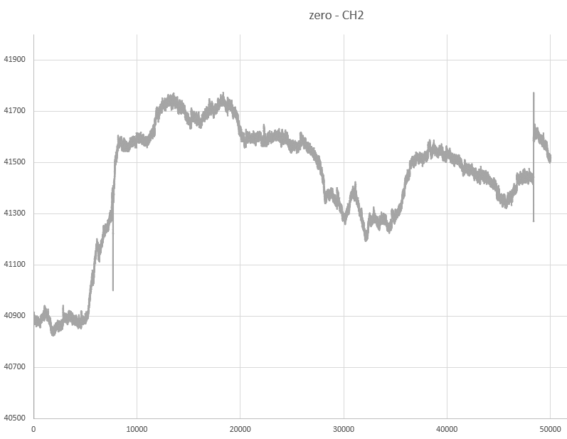
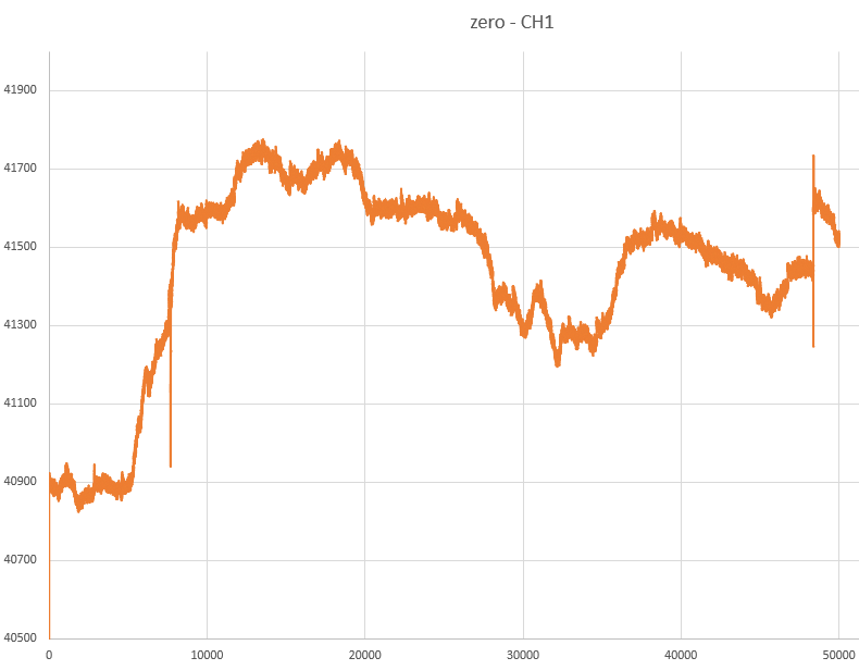
At first glance data looks very promising! Huge voltage variations are seen when IC is stressed, but long-term data capture shows some flaws of this appriach to building weight scale. Both channels of op amps are closly tracking each other voltage, but mean value between them and calculated values separately drifts noticeably over time. Readings below were captured with load of 253g over 5mins:
![]()
![]()
![]()
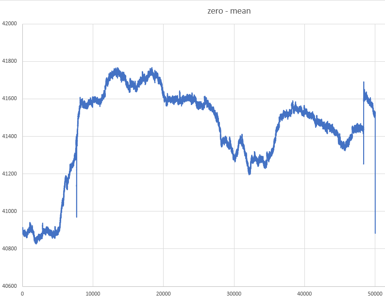
And here are measurements without load:
![]()
![]()
![]()
Close resemblance between both channels can be seen and if noise is accumulated then channels would not track themself. So my guess is that temperature is culprit here as both ic's are close to each other so their temperature should be almost identical. Oven stabilisation may be a little overkill for this purpose, i hoped that offset drift would be symmetrical as opamps are glued in opposite directions but it is not the case - maybe different channels have transistors oriented in such way that it would produce reversed signal?
-
Second try
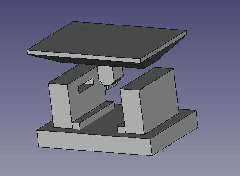
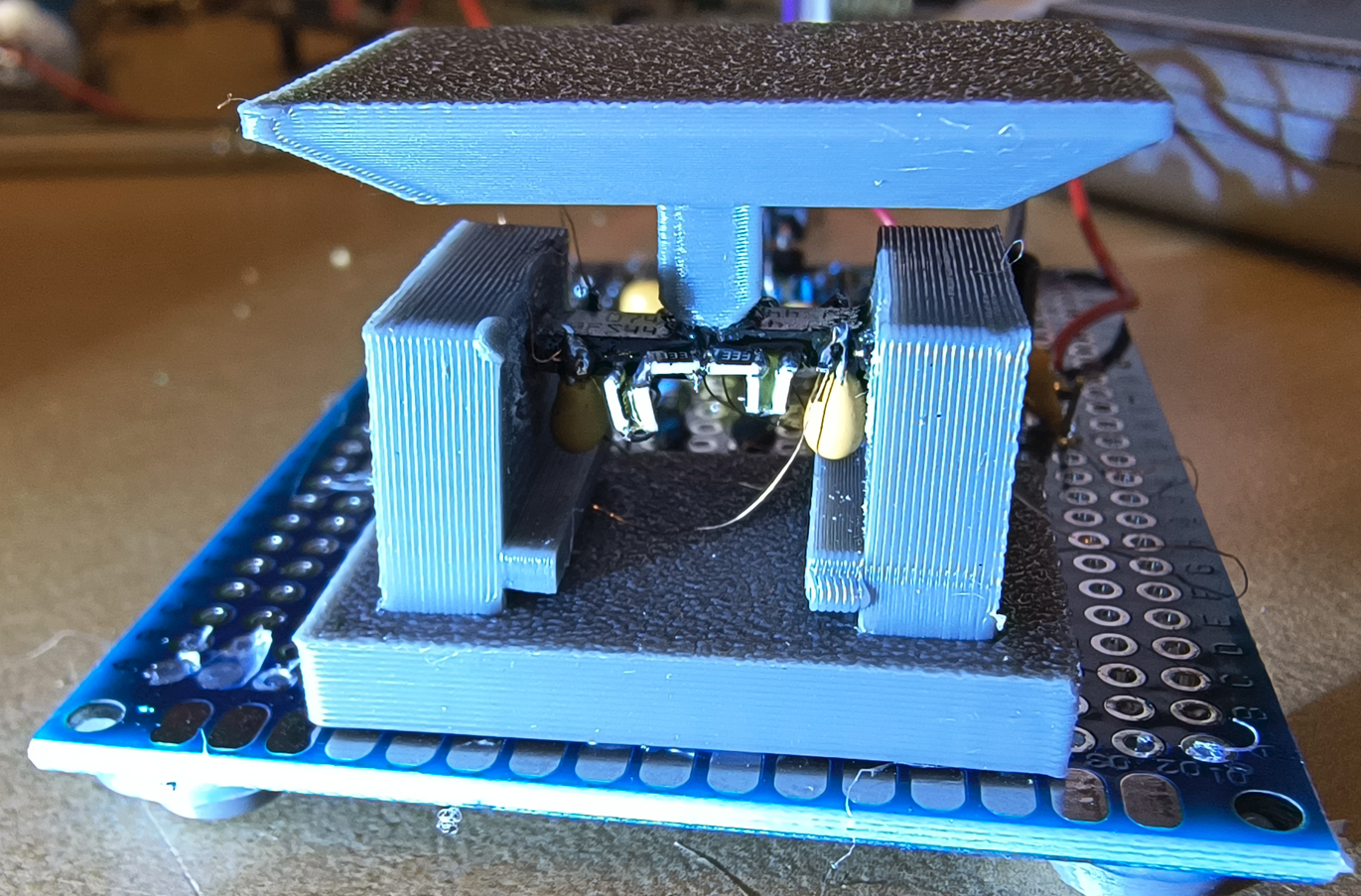
10/20/2025 at 12:56 • 0 commentsMechanical stability was huge issue in previous prototype - glue has too little surface area to bond corretly to IC's package. So second prototype was designed and built - this time platform is supported by two IC's which made it much stiffer and enabled putting heavier weights than previously.
![]()
![]()
Second prototype is bonded to protoboard with hot glue, also I added some cone-shaped legs because solder at bottom side prevented whole contraption from standing straight. This time two op amps were connected, also i added RC low pass filter made from 2K resistor and 100n capacitor to filter some higher frequencies. Op amps are connected with thin magnet wire pulled out from defective relay. It works great and ensures that wires do not make any mechanical stress of the internal die. Unfortunate side effect is susceptibility to radio waves, during data capture whole contraption in big tin can for shielding.
During measurement i also checked if temperature is influencing data and it is, but effect is much less noticeable than putting 50g (25g per IC) of "load".
Why IC manufacturers are assuming that end users can load their products only in electrical terms?
-
First try
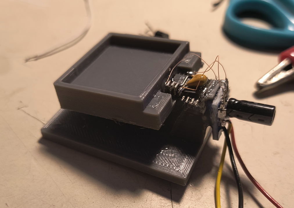
10/20/2025 at 12:24 • 0 commentsFirst try was made as simple and quick as possible. I designed and 3D printed stand and shelf connected by carefully selected AD824 from scrap pile. This device won my casting for bending as it works happily with low voltages and have long, thin packaging. Most importantly this device is FET-based so loadcell effect should be noticeable - Bob stated that effect is strongest in BiFet devices, but other sources mentioned that FET's also are sensitive to mechanical stress.
Before gluing package was filed a little to make package more flexible.
Measurement circuit is very simple with both inputs connected to ground via 10R resistors and 10k between negative feedback to output. This gives 1001 amplification of voltage offset at output.
![]()
Unfortunately i forgot to make more photos with DMM of this stage, so just trust me that output voltage was susceptible to bending IC :)
OP-AMP Weight Scale
Bending IC's to measure weight - Component Abuse Challenge 2025