Gilhad
-
FORTH 25.01.13 HW considerations
01/13/2026 at 21:34 • 0 commentsThere are many strategies, how to implement FORTH, but I will refer mainly to Moving FORTH from Brad Rodriguez, author of CamelForth.
Pleas read the Moving FORTH alongside with this log, as I will just answer or paraphrase questions laid there, without reapeating everything
16 bit or 32 bits? 24 bits! and CELL size:
Target platform is ATmega2560, which has this types of memory:
- Flash 256kB (code may be executed only from here, not writable (simply))
- Internal RAM 8kB (may be extended to 64kB)
- External RAM 128kB (part used to extend RAM)
- Shared RAM 128kB
To address all types in pointer is needed at least 20 bits, so I will use CELL size 24bit (3 bytes, 3 registers) for arithmetic and pointers.
THE THREADING TECHNIQUE:
Code can be executed only in flash, which is not (simply and repeatadly) writable, while new data can be only stored in some RAM. So new (user defined) words must be placed in RAM and therefor cannot contain executable code. Only ITC (Indirect Threaded Code) allows it (and I like it most too). Also as NEXT is here long, then JMP to NEXT is way for me. And Token threaded code needs the table allocated in RAM to contain the tokens, which consumes RAM and limits number of user defined names (they use the token space too) so I will not use it.
Intermezzo:
- Primitives are words written in assembler (or so), the basic words like + - @ ! DUP DROP
- Compound words are words written in FORTH, eg. : DOUBLE DUP + ;
- Phrases are words, that would normally be coumpoud, but I choose to write them in assembly instead ( eg. DOUBLE: add r2,r2; adc r3,r3; adc r4,r4; NEXT;)
In current stage of implementation it looks, like NEXT would take aroud 70 clocks (~4.4 μs) so DOUBLE as compound have 3xNEXT and some code, DOUBLE as phrase have 1x NEXT, and 3 clocks code (which is shorter, then any code in compound DOUBLE). I will use phrases for many usual combination of words (yes, phrases), like 1 +, 1 CELL +, ... as well as for some more complicated parts.
While Flash is little slower than internal RAM, there is a lot of it and RAM is also needed for graphics, file operations, stacks, variables, etc. etc. so I want to prefere Flash to store as much of usual load as possible (common words, vocabularies ...).
Things in Flash must be compiled and uploaded before use whith the rest of FORTH code (~slow and complicated Arduino way).
Things in RAM may be easily changed anytime (added, edited and deleted).
Primitives have native code in flash obviously.
Phrases are just more complicated primitives and so are in Flash too.
Compound words may be placed in RAM at runtime, or placed in Flash at compilation of FORTH as data, like this:
- DEFWORD w_DOUBLE,0,"DOUBLE",f_docol
- PTR24 w_dup_cw
- PTR24 w_plus_cw
- PTR24 w_exit_cw
Some words (like words using CREATE DOES> ) needs executable part, so such words have to be compiled into Flash.
If compound word's definition contains any IMMEDIATE word inside, then such word have to be resolved before it may be compiled into Flash. (All the IF-THEN, BEGIN-UNTIL and other constructs.)
End od intermezzo
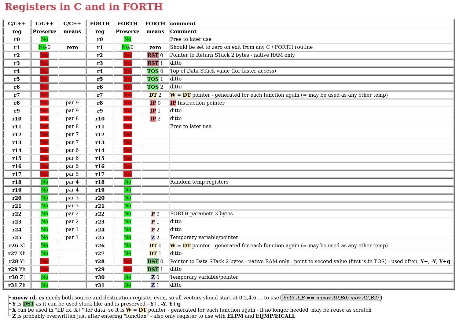
REGISTER ALLOCATION
- In my previous FORTH implementations I used NEXT in type DT=*IP++; JMP *DT++; and DT was the use as pointer to data part of word. On Brad pages is used W for the same function.
- On ATmega only Z(r30,r31) may access Flash, so it will be universal scratch pointer for everything, r25 is used for selecting data source and bank.
- One ATmega pointer (Y(r28,r29), 2bytes) is preserved by C and Data Stack will be in Internal RAM, 2 bytes are enought.
- pointer X(r26+r27) + r0 will became W=DT pointer, as it is generated for each function again and again and used as scratch,
- TOS will enable faster access to Top Of Stack, as many primitives (@, !, ...) and phrases (1+,1C+,...) may use the registers and not move stack at all.
- Return stack (r2,r3) will point also only to Internal RAM, so 2 bytes are enough
- HW stack pointer will be used as stack for C/C++ routines, like SD card readers a interrupt handlers (which is not FORTH part of system) There are none simple means for addressing relatively to it.
- I did not decide, if I will need UP=UserPointer, this may wait for now, r11+ are still free
- Also I will use some Canary value to see how much of stacks was used and C/C++ routines would affect this substantially. (Canary ~ CACARY ~ 0xCACAA7 seems usable and maybe routines for debug prints will translate it to special string "Canary" for easier spotting inside FORTH 3B stacks)
- for other space, then 3 byte stacks I will use 0xDEADBEEF instead as it is simple to alling to 4 and reversly test mod 4
- note, that moving pair of registers need both source and destination registers to be even numbered (0,2,4,...)
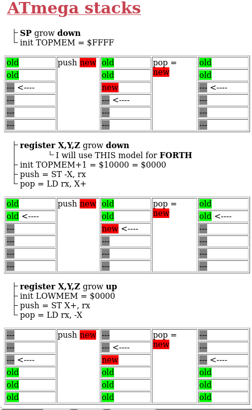
Here is my register allocation (also classical C API) and possible stack implementations on AVR:
![]()
![]()
Best of stack implementation are for me register stacks growing down, as the stack pointer points on lower byte of the value and is easy to manipulate.
DOES and company
In Part 3: Demystifying DOES> are discussed words like CODE; or DOES> which compiles native code into new words. This is complicated on ATmega2560.
Such words may used to define new words, but the new words will not work as they are in RAM. But the new words may be dumped and transformed into Flash compatible byte defintions, which may be then compiled into FORTH and uploaded as new program.
So I will build my FORTH with lot of such words in the core, either as compound words or as phrases.
See also How do you build a Forth system for the Very First Time?
-
FORTH 25.01.10 Intro
01/10/2026 at 13:37 • 0 comments![]()
FORTH is interesting language, especially for embeded systems. See wiki, get book Starting FORTH, or find any other resources. It is used in critical places, see Forth in Space Applications.
FORTH is a stack-oriented programming language and interactive integrated development environment designed by Charles H. "Chuck" Moore and first used by other programmers in 1970.
FORTH uses stack and Reverse Polish notation (RPN) instead of infix notation, so it does not need brackets for evaluation equations and functions can have any number of input parameters as well as any number of output parameters.
Infix: ( 1 + 2 ) * ( 3 + 4 ) * 22 - try to explain in details, how this should be computed
Postfix: 1 2 + 3 4 + * 2 SQUARE * - take 1 and 2, add it, take 3 and 4, add it, multiply the results, take 2, square it then multiply the results
Maybe you will use postfix to explain infix notation :)
The 1, 2, 3 and 4 are numbers, they are simply put onto stack.
The +, * and SQUARE are all words (how FORTH calls functions and subroutines) and each take 2 parameters from stack and return 1 result.
(Word C@ (character at) get address from stack, read charecter from there and put it on stack (~PEEK). Word C! (character store) read address from stack, then read character from stack and write it to the address (~POKE). Words AND, OR and NOT are binary &, binary | and binary negation. )
New words are usually defined by colon : followed by new_name then words to make the function and finished by semicolon ;
For example, on ATmega based Arduino (like UNO, Nano, Mega) the system LED is attached to port B, pin 7, which Arduino calls D13. So we can define some usefull words like this:
: SetupLED DDRB C@ bit_7 OR DDRB C! ; \ read direction flags of port B, set 7. bit on and write back, ~ pinMode(SYSTEM_LED,OUTPUT);
: LED_ON PORTB C@ bit_7 OR PORTB C! ; \ read port B, set bit 7 on and write back ~ digitalWrite(SYSTEM_LED,HIGH);
: LED_OFF PORTB C@ bit_7 NOT AND PORTB C! ; \ read port B, set bit 7 off and write back ~ digitalWrite(SYSTEM_LED,LOW);
: LED_CHANGE bit_7 PINB C! ; \ write bit 7 to PINB so the output just change value ~ digitalWrite(SYSTEM_LED, ! digitalRed(SYSTEM_LED));
The usual routine with INO files is, that you
- make change in INO file
- save it
- compile it
- upload it (Arduino restarts)
- get to the point, where change should manifest
- observe it
- see what else need change
- start from begin
When FORTH is installed, you have interactive shell so it goes different way:
- - open Serial connection to Arduino
- use some words
- see what need change
- write new word or edit old one
- repeat
In both ways you have to write new commands, but with FORTH installed you do not need to compile, upload (which restarts Arduino) and then again set Arduino to required state. You just use the new word immediately, without reseting Arduino at all.
When debugging some circuits and modules (maybe on breadboard), where you need set some pin high in middle of long test, it is really convenient to just do so, without all the recompiling and restarting everything again and again.
I found it really convenient when I needed to test some connections on breadboard, where some wire was just loose, or misplaced. Also I wrote some more complicated tests on spot and reused them as many times as was convenient.
When some words are use more often, they may be saved in file on PC/NB and then simply copy-pasted at begin of every session, or if you serial program allows it (like picocom, which I use and recomend) simply send as file over the serial.
And they may be added to the FORH vocabulary permanently, but it need FORTH recompilation and reupload, so it is better to do it with already debugged and fully tested words.
-
Freehand use
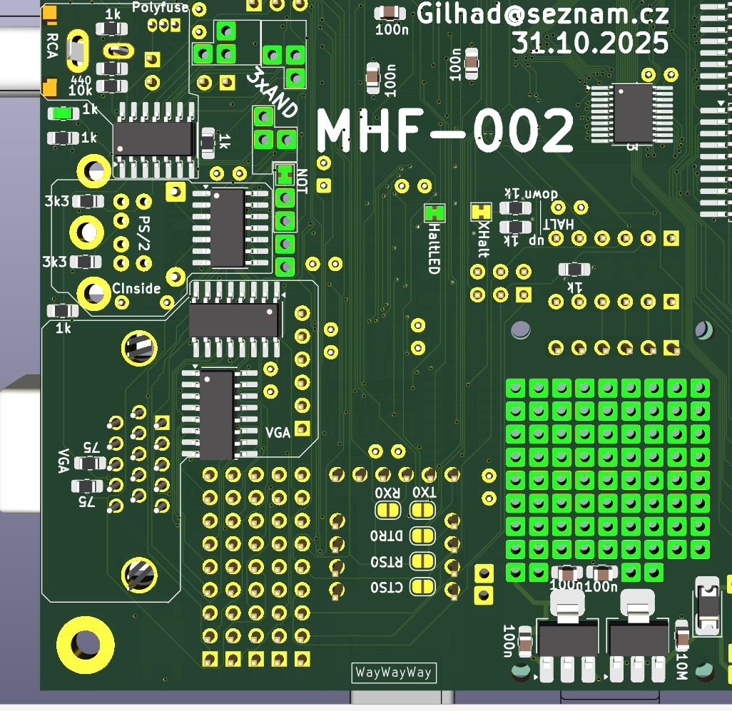
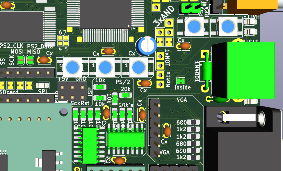
01/09/2026 at 00:26 • 0 commentsThere are unused 3 AND, 1 NOT and another 1 NOT + LED may be recovered at expense of HALT visualisation.
Also under SD card module is 8x9 free THT soldering points accompanied by +5V, +3V3 and 2 GND.
All MCU pins are avaiable on connectors as well as lot of internal points.
That can be used for adding custom connections, HW and functionality, if needed.
![]()
-
SystemBus
01/04/2026 at 18:14 • 0 commentsThere are two copies of SystemBus, both paralely conected. Either one, or both may be used to stack with other PCBs like retrocomputer or another cards together. I will use female/male connectors (socket with long legs) in the inner position, but it is also possible to use pins downwards and socket upwards, alternation positions, if the F/M connectors are ont available or practical.
The SystemBus contains the usual common power, 8bits Data and 16bits Address, then communication with GLUE divided to A and B parts and rest of pins is reserved for signals (like MasterReset).
MasterReset is used for reseting all connected PCBs, while normal Reset resets only this PCB without affecting others.
![]() |SystemBus-schema.png|
|SystemBus-schema.png|![]()
|SystemBus-side.png| view from side with sockets in outer and pins in inner holes
-
Configuration
12/28/2025 at 15:01 • 0 commentsThis PCB can be used in different ways and different configurations. There are a lot of solder-jumpers (some open, some bridged by default) to customize it for your needs.
Serial connection
RX/TX are on pins PE0/PE1, CTS/RTS are on pins PB4/PB5, all 4 are at their respective ports pins. DTR is connected to Reset block directly.
Together they are on Serial connector on top edge for connecting any external Serial source (default).
![]() |USB-Serial_pinhead.png|
|USB-Serial_pinhead.png|Solder-jumpers there enable connection to CH340G USB-Serial convertor.
![]()
|USB-Serial_CH340G_top.png|
Another set of Solder-jumpers is under CP2102 module and allowe use of that module.
![]() |USB-Serial_CP2102_bottom.png|
|USB-Serial_CP2102_bottom.png|CH340G and CP2102 cannot be used together, or with external Serial (signals will conflict).
SBC config
To use Shared RAM in SBC configuration is needed access to its signals (otherwise managed by GLUE) and maybe to its gates to SystemBus too - simply solder all jumpers in this part and use the new scheme
![]()
|Shared_RAM_top.png|
![]()
|config_SBC.png|
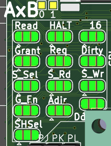
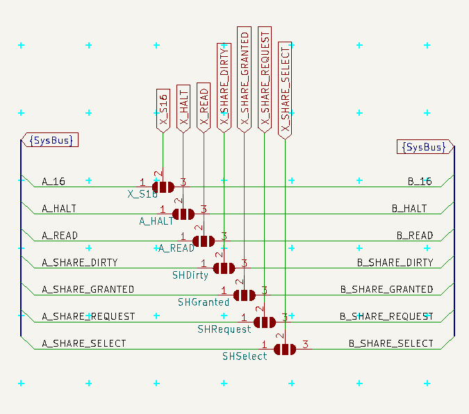
AxB SystemBus connection - Graphic Card
Graphic Card configuration is the final goal - this PCB would serve as Input/output for retrocomputer - SystemBus is connected to other PCB, where is retrocomputer and its GLUE is managing Shared RAM and some more signals.
There may be 2 such cards in system (one for VGA/RCA where screen takes 90% of time, other for SD card, PS/2 and Serial, where some transmission needs be uninterrupted by screen). One card will be named A and other will be named B and GLUE will talk to each separately. To became Card A solder left part of each of 10 jumpers, to became card B solder right part. (And in both cases unsolder SBC configuration.)
![]()
|config_GLUE_top.png|
![]()
|config_GLUE_top_A.png|
![]()
|config_GLUE_top_B.png|
![]()
|config_GLUE.png| This is communication from MCU to GLUE.
![]()
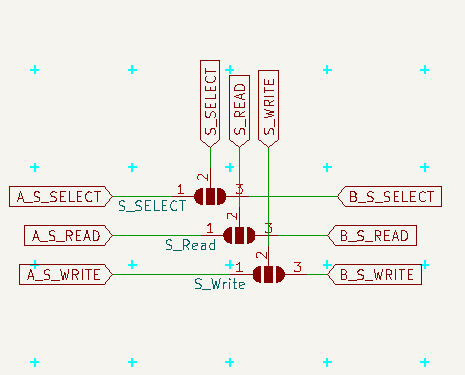
|config_gates.png| Here is communication from GLUE to gates
![]()
|config_shared.png| and here communication from GLUE to Shared RAM
Notice, that in order to read/write shared RAM the MCU need ask GLUE to set related signals (and GLUE will do it only if the Shared RAM is owned by MCU)
HALT + LED
For proper boot of retrocomputer may be needed to fill its RAM with the "ROM" part before it is started. To do so the HALT should be pulled DOWN (it is active low) and hold there until is all ready.
If this PCB is supposed to do that, it would be good to solder pulldown resistor (and not pullup), after boot actively hold down the line and after setting the RAM (open gates via GLUE, manipulate A0..A16 and D0..D7 and set write signal via GLUE) hold it UP.
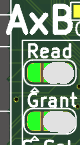
If this PCB is suppose to do that, but does not want to doo it, solder pullup resistor (and not pulldown), cut the XHalt jumper and use HALT LED for anything else (like SYSTEM_LED, but beware, it is also active low)
If this PCB is not suppose to do that (the other (AxB) card should do it), do not solder any pull* resistor, cut the XHalt and use LED as you want.
On SBC configuration this line is used to to write to Shared RAM, so do not solder pull* resistors, do not cut XHalt, but you may cut out the HaltLed or leave it to indicate writes to Shared RAM.
Also you may cut the HaltLed and solder any output to this inverted LED or use the invertor for anything else.
![]()
|config_HALT.png|
![]() |config_HALT_bottom.png|
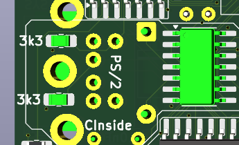
|config_HALT_bottom.png|PS/2 Direct access + Inside
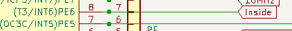
If you want read the PS/2 direct and process it, solder the 2 jumpers near SPI/SD card (and change the two marked resistors to 1 kOhm ) Also you may want to cut the Inside jumper, as it is probabelly of no use in such scenario. It also interfere with SPI, which needs address in SW.
![]()
|PS2_direct_top.png|
SD Card
SD Card may be cut off SPI and managed separatelly via its header, but it is probabelly of no use
RCA source 40 x 80
This pinhead selects source of graphic data for RCA - the pins are 40,signal,80 and the center (signal) should be connected to one of the sides - 40 selects the UART1 output (and classical driver with 40 characters per line), but I want to test sending there data in similar way as for VGA, so the 80 selects output from VGA module (which may or may not be able to provide 80 characters per line). Now I recomend to use 40.
-
Debug LEDs
11/18/2025 at 19:01 • 0 commentsAs I need feedback while testing things, I usually use LEDs on Arduino, but LEDs needs IO pins and forgotten code may affect function later, so I decided to use one pin (PD4) for 6 Neopixel WS2812B which are serial driven. Setting different colors may indicate different states and should I accidentally forget somewhere some testing code, it will reveal soon and in non harmfull way.
---------- more ----------They share pin with X_SHARE_GRANTED signal, but it should not be problem, as this signal is input for MCU and LEDs are output and both are separated by resistor. GLUE, which set this signal does not read it, so it will not be bothered with data for LEDs and LEDs need some specific protocol, so they will ignore ocassional changing in the signal.
My plan it to dedicate some RAM for the values of these LEDs and simply let system resend it after each screen (60 times per second), so programs will just put values there and forgot it (like with videoRAM),
Here is the scheme
![]() Debug LEDs are only on top of PCB (and I did not found more place for them, so I did not place there more of them). There are their numbers, you may populate just few with lower numbers
Debug LEDs are only on top of PCB (and I did not found more place for them, so I did not place there more of them). There are their numbers, you may populate just few with lower numbers ![]()
-
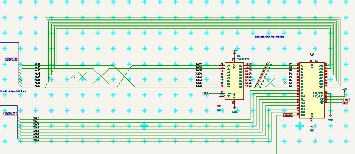
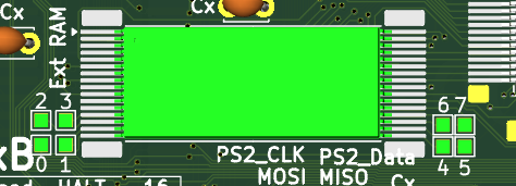
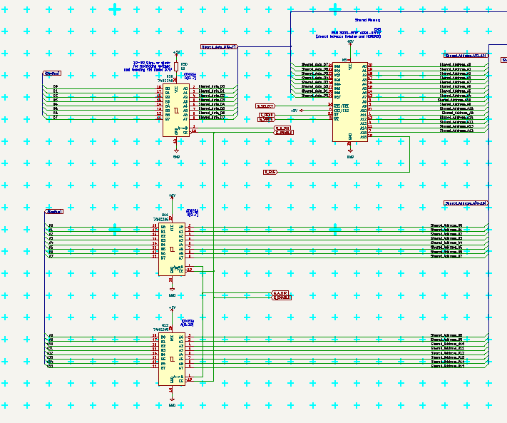
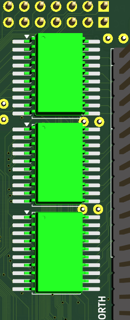
RAM (External + Shared)
11/15/2025 at 06:18 • 0 commentsExternal RAM may be used to have visible 64kB RAM inside MCU (but those 56kB extra is 1 tick slower to access).
Shared RAM may be shared with retrocomputer or used as just storage with slower time then RAM but faster then anything else.
Both are 128kB chips CY7C109D, as I found them to be cheap, accessible and 5V friendly. The truth is, that their output is lower then 3.4V, but Atmega should be able use it anyway. 74HC245 gate may need power little lower than +5V, so I added resistor there to slightly decrease it (or maybe Schottky diode). I will see, if it is really needed.
Note that near the RAM datalines may be permutated any way, as well as adderss lines, because it does not matter, the permutation will negate when the data are readed back. So it may be used to have better physical traces there (as I did).
---------- more ----------External RAM is connected to ports PA and PC, where PA is latched by 74AHC573 fast octal D-latch. It must be enabled in SW and managed by PG0-2. I will use PG3 to select in which half of chip it resides.
It can be accessed also manually if the automatic is not enabled, by setting low address to PA, latch it and then use PA as data line. This way any byte in 128kB may be used at slower access time. I will probabely use it for futher expansion of FORTH memory. those 8 squares around it are probes of D-latch output, so it could be tested too. D-latch is placed under the PCB to have short lines to RAM.
![]()
![]()
![]()
Shared RAM is connected to ports PJ, PK and PL, and in graphic card configuration is managed in cooperation with GLUE. In SBC configuration the MCU need to manage it itself, so all SBC solder jumpers should be soldered. If output to System Bus is not needed, also gates may be unpopulated.
![]()
![]()
![]()
-
SD Card + SPI + ISCP
11/15/2025 at 05:27 • 0 commentsSD card formated with FAT system serve for storing and reading files.
Currently it uses SPI and Arduino library, but as I use timers, I update millis() just each screen refresh to make illusion of time for its timeouts.
SPI have its LED and pinheader placed near SD card and may be separated by cutting solder jumpers (default connected). MISO/MOSI may serve also for PS/2 serial input when its (default open) solderjumpers are solrdered.
ISCP connector is also there with pin 1 marked by white rectangle under SD reader.
---------- more ----------![]()
ISCP is ATmega/Arduino Standard and may be used for programming MCU. As there is not much space free, the Silkscreen is placed above (+5V GND), bellow (white mark visible from angle under SD card reader, Sck and Rst) and by sides (MISO left down, ISP right) for correct orientation of connector.
SD Card Reader may be cut out for freeing CS/SS PB0, or other pin may be used for SPI chip select.
SPI LED is connected to SCK and placed just above SD Card Reader near the SPI pinheader.
SD Card Reader should have level shift to 3V3 and fixed CS to disable MISO, when not active. See my comments here and original discussion.
![]()
![]()
(only resistor for LED visible here).
I tried classic Arduino SD library for reading SD card and it works, but need somehow advancing millis(), so I just incremented the value in VGA library. Also I tried only to read one byte at new screen, as I did not know the timing of the library, which was slow, but worked. I will make my own version with much better approach some time later (I hope).
-
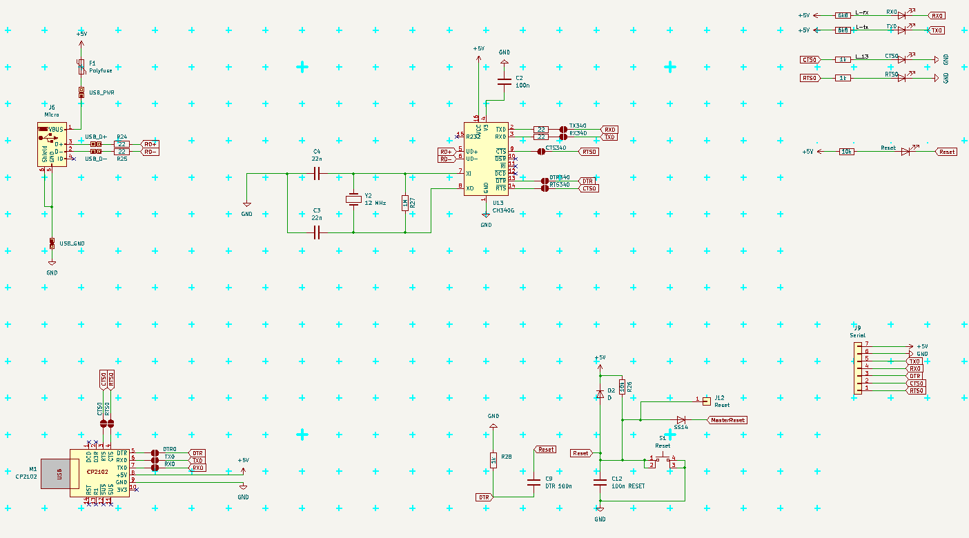
Serial + USB
11/14/2025 at 19:36 • 0 commentsCommon
All marks are from MCU signal side of view. (RX is input, TX output, CTS is input, RTS is output, DTR is input).
Default Serial uses USART0 (RX0/TX0 - PE0/PE1 pins) and RTS/CTS (PB5/PB4 pins) and DTR connected to Reset.
There are 3 possible sources for Serial Communication
- Serial pinhead - always conected to MCU, need all signals to be attached
- CH340G with micro USB from Arduino Mega Pro - need to solder connect (RTS/CTS does not work with usual drivers)
- CP2102 module with USB A - need to solder connect
There can be two modes of communication
- full with RTS/CTS flow controll - recomended - protect agains buffer overflow, when PC transmits more data (like a file, or Copy-Paste larger block)
- simply RX/TX like on Arduino, buffer may overflow, cannot paste longer lines
---------- more ----------For RTS/CTS the pins must be connected and driver must use it.
Connect RX to TX on of the other part communicating (USB-Serial module, PC, other Arduino ...).
(And TX to RX; CTS to RTS; RTS to CTS; DTR to DTR.) Typical crossing of lines.
The Serial pinhead is already connected to MCU.
CTS is "Clear To Send" and is INPUT, when is low, MCU can send data over TX, when it is high MCU should not send anything
RTS is "Ready To Send", (in new era it is RTR "Ready To Receive") and is OUTPUT, when is low, the other side can send us data, if it is hight, the other side should stop sending
If buffer is too full, set RTS to HIGH until the buffer is empty again.
(It is critical to good communication, as PC have gigabytes of memory, large buffers and fast communication, while ATmega is realitively slow, have small buffer and processing data may take some time. So we need temporaly stop PC from sending more, until we can receive it.)
![]()
Serial pinhead
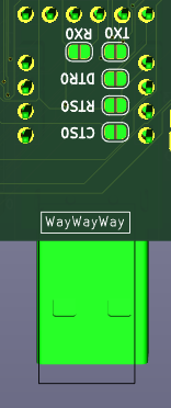
It is "easier" Serial connection as it is just pinhead. It contains all the signals and what is there connected is up to user.
There are LEDs for RX, TX, RTS, CTS near micro USB connector, so communication should be visible. RTS and CTS LEDs are active when the signals are HIGH, which means the direction is BLOCKED. (So use of red LEDs make good sense here.)
DTR is near Reset buton, and does not have LED, the Reset LED indicate any Reset
![]()
CH340G
This came from Arduino Mega Pro, where RTS/CTS are not used. If you prefere this behavior, solder only RX, TX and DTR jumpers.
There are problems with drivers for CH340G using RTS/CTS, if it does not work, look for some patch or different driver.
I had problem with the Micro USB connector, that it does not had good and reliable contact and was too easy to damage/rip off. So I added some pinholes for its pins, so I can solder piece of PCB with USB A connector there when problem arise. There are actually two lines of holes, one connected to Micro USB, annother connected to CH340G chip. They are connected on BOTH sides of PCB, so to cut it would need cut on BOTH sides. (I do not think, that it would be needed anyway.)
In case you want use this connector for power only, then populate only the connector and polyfuse (or cut the D+ and D- on both sides of PCB)
![]()
![]()
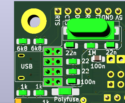
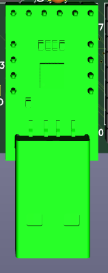
CP2102 module
This module have all signals connected to pins, and have solid USB A connector. To use this module for communication, solder the jumpers on the bottom side of PCB. To use it just as power souce, simply solder the module in.
![]()
![]()
Notice, that signals should came from max one module at time, so solder/desolder and cut the solderjumpers as needed.
Also notice, that normal Arduino Serial does not use CTS/RTS signals, so in this case is better leave them unconnected.
Also notise, that RTS/CTS flow controll usually need be allowed on the PC side in communication program (Serial terminal and so), Arduino IDE cannot use it at this time.
-
PS/2
11/14/2025 at 08:02 • 0 commentsErrata
- all 10 kΩ resistors in PS/2 (8+2) should be rather 1 kΩ (otherwise it take too long for reading values, like 10 clock cycles)
PS/2
PS/2 have 2 lines - Clock and Data. See https://wiki.osdev.org/PS/2_Keyboard
Clock runs at 10-17 kHz, 11 pulses (normal High, active LOW), data came as
- 1 start bit (always 0)
- 8 data bits (least significant bit first)
- 1 parity bit (odd parity)
- 1 stop bit (always 1)
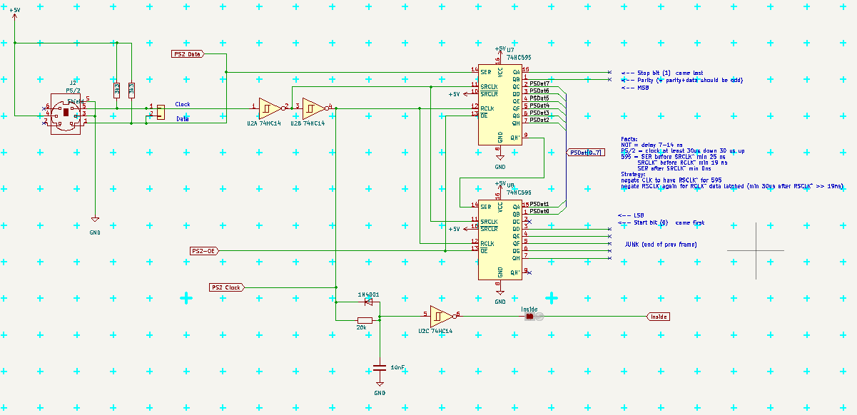
The clock/data can be connected directly to PB2/PB3 MOSI/MISO via solder jumpers (default OPEN, solder to USE) and decoded as serial communication, but I will use two shift registers and R-C to detect, if we are Inside the packet or not, so I could read the data as one byte on port PF, when I do not use it as VGA data output.
Inside signal (connected via closed solder jumper, cut if not wanted) is HIGH when clock is changing, LOW, when clock stops and PSDat is valid.
PS-OE is active LOW and let the captured PS data go to port PF
---------- more ----------(In next version I may redirect PS Clock BEFORE fixing its edges by Schmitt 74HC14, so it would be possible also send data like status LEDs (Caps,Num,Scrl) to keyboard)
The plan is to check at end of VGA line, if the Inside went LOW, then set port PF ro read, set PS2-OE LOW, read PF and set PS2-OE HIGH again. Inside is way longer than VGA line and pause between two PS/2 blocks is also long enought for it.
The schema is distributed over more places.
The main part with shif registers:
![]() Connection to data:
Connection to data:![]()
Inside signal:![]()
Serial clock+data signals:![]()
Top PCB:![]() Bottom:
Bottom:![]()
MHF-002 (Mega Home FORTH)
ATmega2560 based SBC with VGA, PS/2 and SD cards - meant to run FORTH now and serve as graphic card later.
 |SystemBus-schema.png|
 |USB-Serial_pinhead.png|
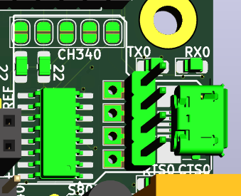
 |USB-Serial_CP2102_bottom.png|


 |config_HALT_bottom.png|
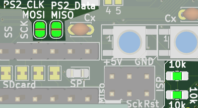
 Debug LEDs are only on top of PCB (and I did not found more place for them, so I did not place there more of them). There are their numbers, you may populate just few with lower numbers
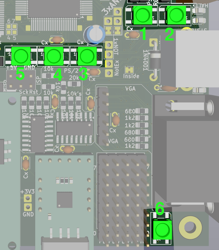


 Connection to data:
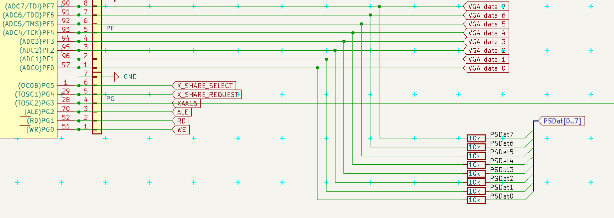

 Bottom: