 Gilhad
Current status:
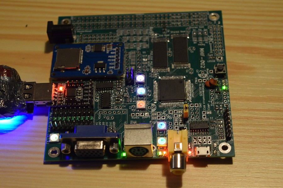
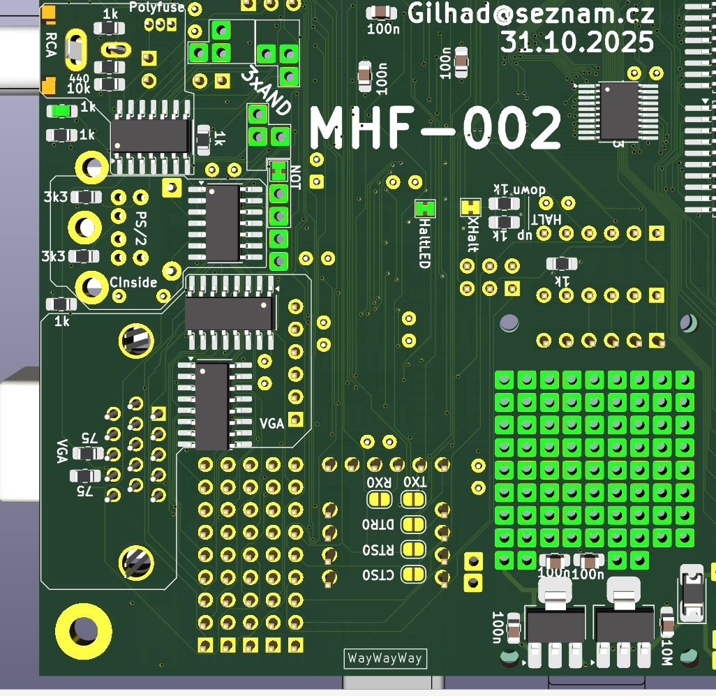
MHF-002 PCB arrived, all modules (except gates) are successfully soldered and tested, now I need to change tests to libraries and combine it all together. Also I need to write better FORTH engine with enhanced 24bits pointers to be able address full External+Shared RAMs. More ideas about VGA + RCA output are to be tested too.
Older:
MHF-001 proved, that VGA signal can be generated clean and stable. Due bad PORTs assignment was characters little distorted, this should be fixed on this new card. Also I failed to solder the external RAM perfectly, due footprints oriented for machine work, not hand soldering, so it sometime worked, sometime not and preesig it by hand improved the chace for right results. New version have much longer pads on footprints, which I can solder reliably.
More similar improvements was discovered over time, but basicaly I was able somehow confirm all wanted features.
Software needs be rewritten for new port usage and for better functionality. It is just matter of time and effort.
FORTH helped very much, as it allows interactivelly program the atmega over keyboard or serial line, without recompiling and uploading everything from start for any and every action wanted. Interactivity simply rules :)
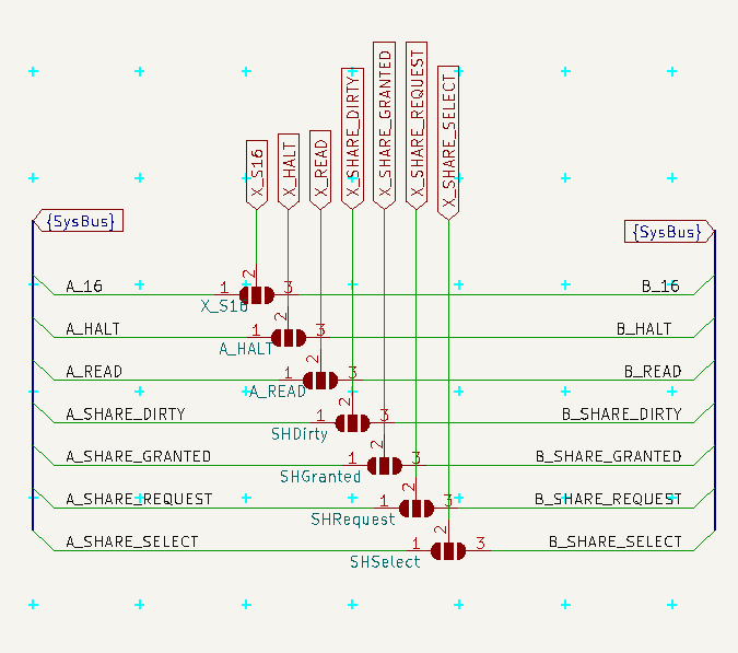
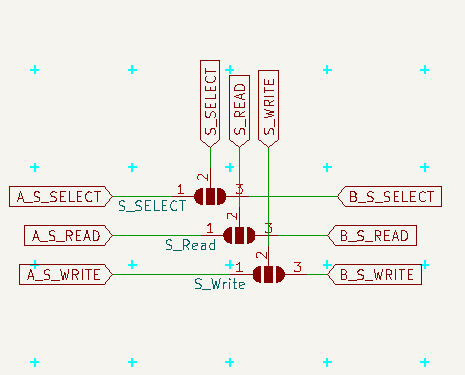
Main idea for this card is to share 128kB RAM with the HD6309 computer, where it will be mapped to one or two 8kB windows and let the CPU fill commands and data in on its own pace, then map the RAM to MCU (ATmega) and read (and execute) everything on its own pace. This will enable high throuhtput at cost of little latency added and paralel work of both systems.
Generating of VGA signal needs like 90% of time on MCU and it runs in Interrupt routine, to provide needed regularity. The rest of time is used for everything else. CPU is not bothered with such details and runs all the time at full speed.
I do work on this project from begining of 2024 (so nearly two years) and it goes forward slowly, but surly. Now I estimate like another year is needed to explore this card and turn to building the CPU part.
 |SystemBus-schema.png|
 |USB-Serial_pinhead.png|
 |USB-Serial_CP2102_bottom.png|

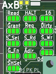


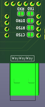
 |config_HALT_bottom.png|
 Ken Yap
 Forthnutter
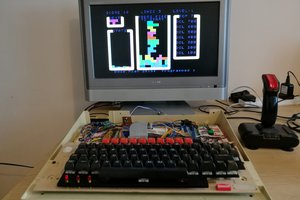
 6502Nerd
 CanHobby.ca