Ryan O'Connor
-
Small Update
12/01/2025 at 17:54 • 0 commentsUpcoming CAM and Microsection Update
I have been reviewing additional layer registration behavior and drill to copper margins on recent HDI and Class 3 builds.
The next update will include a detailed microsection comparison that connects several CAM stage decisions such as pad compensation, mask expansion, and drill offset budgeting to what appears in the finished cross sections.
The goal is to show how small adjustments in CAM influence annular ring, dielectric spacing, and final fabrication yield.
-
CAM Adjustments That Prevent Class 3 Yield Loss
11/24/2025 at 15:48 • 0 commentsThis update adds a brief look at how CAM engineers adjust layout data before fabrication.
Pad growth, mask expansion, trace width compensation, and drill-offset budgeting are applied to prevent annular ring loss, copper exposure, and breakout in Class 3 builds.
A simple before and after diagram is included to illustrate how these corrections stabilize yield.
![]()
-
The Real Tolerances Behind Class 3 PCB Fabrication
11/20/2025 at 16:31 • 0 commentsFive Tolerances That Matter Most in Class 3 Fabrication
PCB CAD tools show fixed numbers and perfect geometry. Real Class 3 fabrication does not work that way. These are the five tolerance behaviors that most often decide whether a high reliability board builds cleanly or turns into scrap.
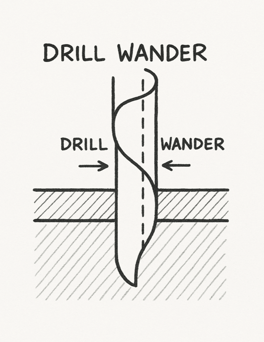
1. Drill Wander
Drill bits do not travel in perfect straight lines. They can walk or bend slightly depending on:
- total stack height
- glass weave pattern
- resin content
- entry material
- drill wear and sharpness
- via aspect ratio
On a pad that is 0.010 inches, even 0.0015 inches of drift can be enough to break a Class 3 annular ring requirement.
If a stacked microvia sits on top of that through hole, the allowed window gets even smaller. Now several features need to land inside one narrow target at the same time.
In CAD, the hole always appears exactly centered. In fabrication, the hole is centered within a distribution that has a real width.
![]()
2. Plating Growth
After drilling, every hole grows copper during plating. The growth amount depends on:
- barrel plating rate
- copper balance across the panel
- tank loading
- current density and field variations
- via density and local pattern
- panel position inside the rack
All barrel plating makes the drilled hole smaller in the final state. That means you do not really get the drilled size. You get the drilled size minus the copper added during plating.
In Class 3 work, where minimum finished hole sizes are tight, this affects:
- press fit pins
- stacked or buried via structures
- component leads that must meet contact rules
- test coupons
- impedance and reference vias
A finished hole that is only half a mil smaller than intended can push a connector or a critical via out of specification.
3. Lamination Movement
During lamination cycles, several things are happening at once:
- resin flows and fills gaps
- copper expands and contracts with temperature
- prepreg softens and then sets
- layers can shift relative to tooling pins
- glass weave can steer movement in preferred directions
On a simple two layer board, total movement may stay small. On a Class 3 rigid flex or complex HDI stackup that goes through several lamination cycles, movement can accumulate.
Registration rarely drifts in a random way. It tends to move more in one direction or along one axis due to how the materials and press setup behave. That is why alignment that looks perfect in CAD does not always align that way on a real panel.
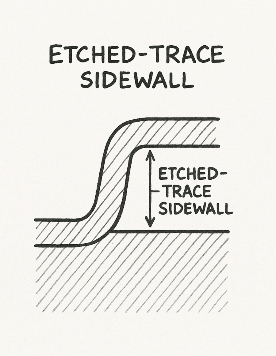
4. Etch Factor and Copper Taper
Etching does not produce vertical copper walls. When you look at a cross section from a Class 3 build, you see that sidewalls are angled. A trace might measure:
- about 5 mils wide at the top
- closer to 3.6 mils at the base
The numbers depend on copper thickness, resist, and etch chemistry.
This matters when:
- impedance must stay inside a tight window
- differential pairs must track closely
- copper balance is uneven across the panel
- long runs sit in regions that etch slightly differently
In high reliability work, this sidewall shape is one of the hidden reasons why impedance shifts away from the value that was simulated.
![]()
5. Material Reality
Material datasheets show clean values for dielectric constant, loss, and thickness. In actual Class 3 production, you see:
- dielectric constant variation across a panel
- resin rich and glass rich regions
- weave skew that pulls fields off the ideal path
- local thickness differences between inner layers
- behavior that changes with temperature and process conditions
A trace that was designed to be 50 ohms with perfect modeling might come out around 46 ohms in one area and 52 ohms in another. You cannot model all of this in the design tool, but you can design with a realistic guard band.
Why Passing DRC Does Not Guarantee Class 3 Success
DRC checks for rule violations in the digital description of the board. Fabrication checks for violations of actual physics and process limits.
Standard layout tools do not model:
- drill deflection
- copper wall taper
- plating variation from panel to panel
- resin movement during lamination
- registration drift over several cycles
- dielectric variation within a sheet
- glass and resin asymmetry in the stackup
- warp under heat and pressure
- stress from repeated lamination and reflow cycles
Class 3 reliability comes from designs that respect these real process limits.
A Practical Checklist for Class 3 Designers
If you want a Class 3 design to move through fabrication with high yield and predictable results, these habits help a lot:
- Use pad sizes that already account for plating shrinkage of the drilled hole
- Increase capture pads on the most critical nets where failure is expensive
- Balance copper on each layer to avoid strong etch bias
- Avoid very long aspect ratio vias unless there is no other choice
- Keep via in pad structures as simple as the design will allow
- Specify laminate ranges and acceptable families, not only a single trade name
- Allow for registration movement on designs that require several lamination cycles
- Budget annular ring based on real fabrication capability, not only the minimum that the CAD tool allows
Most Class 3 issues are not pure schematic or layout mistakes. They are tolerance budget mistakes that only show up once material and process variation are added to the design.
Closing Thought
High reliability boards do not live inside the layout tool. They live in heat, pressure, chemistry, mechanical force, and real materials that move inside real limits.
A clean DRC run is still important, but it is not the finish line. It is the starting point for a chain of steps where small process variations can accumulate.
Understanding those tolerances, especially the ones that never appear on the designer screen, is what separates a Class 3 design that only passes a rule check from a board that also survives fabrication and testing with predictable yield.
If you have seen different behavior in your own builds or want to discuss specific cases, add a comment below. I am always interested in how these effects show up in other environments.
Five Tolerances That Matter in Class 3 Fabrication
Class 3 PCBs fail when real fabrication tolerances stack up. Drill wander, plating growth, and lamination movement decide yield.