 Pavel
Pavel-
VGA output
3 days ago • 0 commentsThe Tang Nano 9k board has 8 outputs from 1.8V bank available on GPIO pins, which is somewhat odd, and not very useful for general purposes, as these signals could not be mixed directly with signals from other pins, which are all have 3.3V logic level. Thus I decided to use them as VGA output pins (VGA RGB needs voltages in the range between 0 and 0.7 V, so 1.8V outputs are ok for resistor ladder.
At first I thought to make the colors encoding as RGB 332, and use 2 other pins for sync signals, but after some deliberation chose RGB222 -- while now it is only 64 colors, this gives couple of grey shades in addition to black and white (the RGB332 does not have true greys among its 256 colors), and two pins that are left unused could be repurposed to output sync signals.
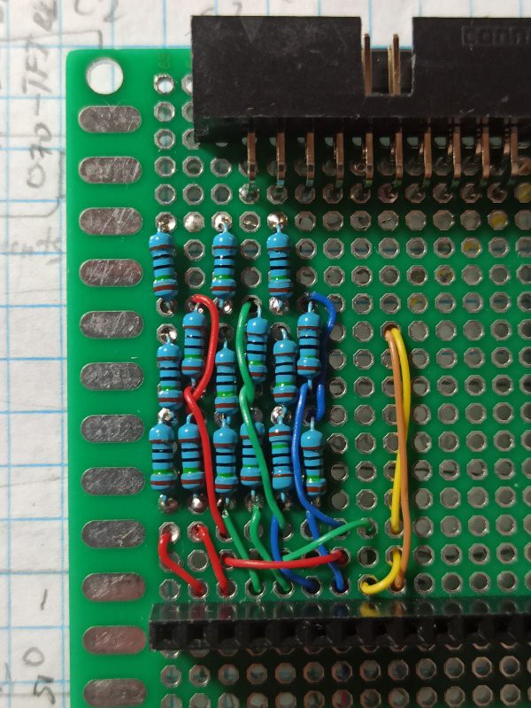
Here is a closeup on resistor ladders (R2R) and wiring before I placed the RGB connector sub-board on it:
![]()
The wires are color coded -- ones carrying RGB signals are in their respective colors, and yellow wire carries hsync, while brown one is for vsync.
I used 150 Ohm resistors here, and wher I needed 75 Ohm, I wired a pair in parallel.Afterwards I placed the connector on top and fixed it with epoxy to the main board:
![]()
------
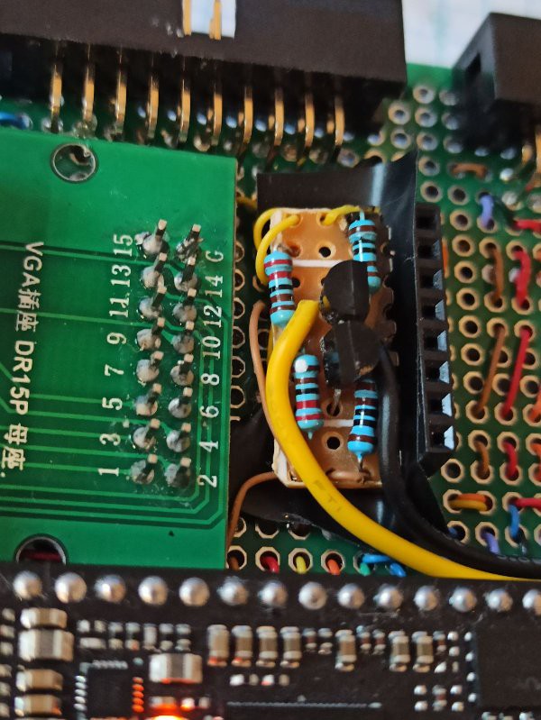
Well, the decision to use 1.8V pins for sync signals brought me some pain: I was sure that the sync signals can be same level as rgb inputs, i.e. 0.7V, and seeing elsewhere that they "tolerate" TTL inputs made me think that up to 5V can be applied, but 0.7V, or 1.8V as I had, would do. Instead it turned to be false, the 1.8V level is barely registered -- the monitor seem to seeing the sync, and sometimes flashed the test pattern for a moment, but most of the time remained dark. The solution turned to be a couple simple RTL inverter gates made from discrete 2n2222 transistor and couple of resistors, much the same as what I started with on the outset of my electronics hobby.
For their addition the sync wires should have been cut, and inverters had to be inserted between cut halves. As I was doing it after the board is complete, at the crowded place where components were held by epoxy, this was not quite easy. Luckily the sync wires weren't embedded in epoxy, and could be accessed, though with some work. The result is a small board attached as shown on the photo:
![]()
-----------
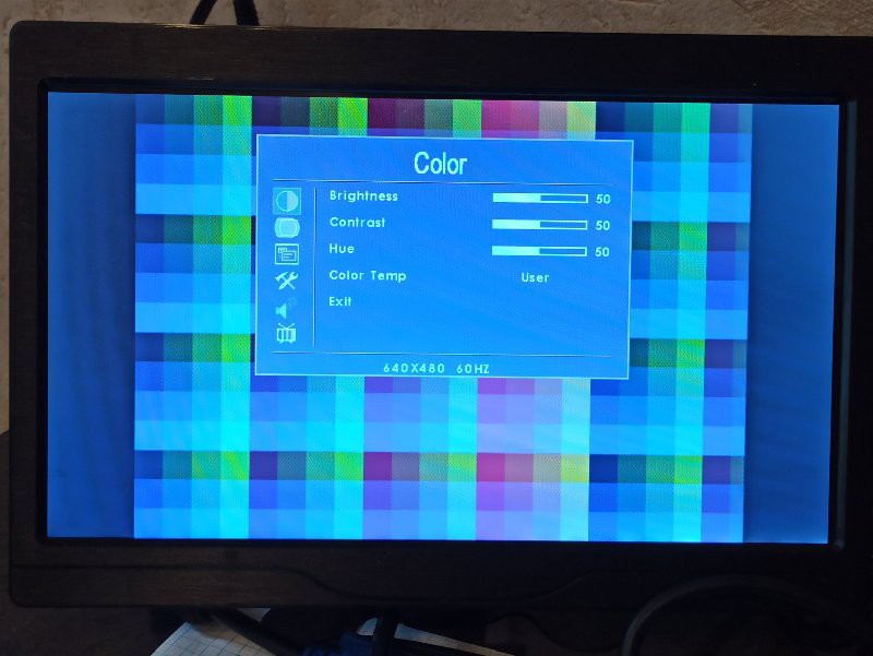
With the problem of sync signals logic levels solved, the test pattern was shown on display right away, and it was rock solid, with sharp edges, in contrast to what I saw when generating such signals with Arduino.
-----------
The VGA timings are calculated for 27 MHz pixel clock, so actual resolution is close to 686 by 480, with rectangular pixels that are slightly taller than their width, with overall picture aspect ratio 4:3, as for the proper VGA 640*480. The timings are correct and display monitor recognizes signal as standard.
![]()
The test pattern is done just by feeding some bits from pixel counter to R and G channels, and from line counter to B channel, giving colored squares 32 by 32 pixels in size.
For deeper dive one can peruse verilog description of simple VGA controller used here.-----
Here is what overall setup looked like:
![]()
-
Testing the keyboard
3 days ago • 0 commentsHere is just a video of keyboard test.
For each button pressed, an individual LED on the row on the left lights up.
------
During testing the works of keyboard, several issues were found - one was that press on one button would be registered as press to it and simultaneously to the one to the left of it, or as it was on the second row, the press was registered on adjacent button instead of one pressed. This turned out to be caused by RC delays due to non-negligible resistance of the buttons, and fairly low resulting current of scan sequence. Adding delay around a microsecond between asserting row address and readin column values remedied the problem.
The second issue was that bottom two rows almost didn't worked at all, except of one button which was working intermittently. The problem turned out to be residing on Tang Nano 9k FPGA board itself, as these lines were connected to pins shared with HDMI output. Those had capacitors connected, and were too slow to respond to changing inputs. To solve the problem, a modification of the FPGA board had to be performed.
------
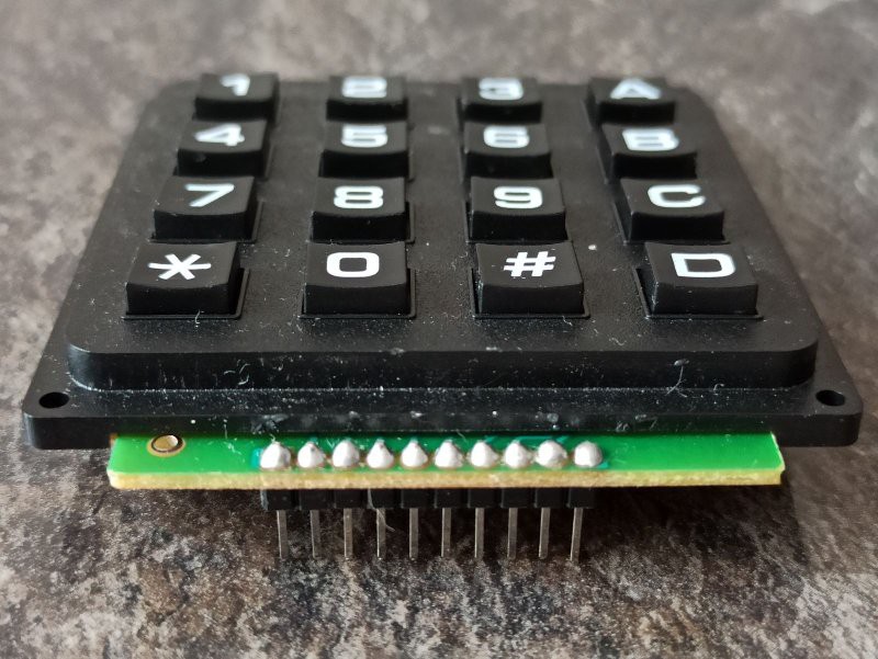
There are 8 pins used for scanning 16 buttons in keyboard, 4 address rows, and other 4 address columns, press on each button makes path between one pin from first group and one from the second group conductive. The contacts on keypresses are not shorts, but have resistances close to 1 kOhm (less when button pressed firmly, more when lightly).Here is closeup on keyboard pins:
![]()
As one can see, there is actually 10 pins instead of 8, but this is due to manufacturer made additional holes in PCB that are not connected to anything. Thus, the pins on the edges are just providing some additional structural support, and have no electrical connections.
------
Verilog description of the keyboard controller is added to files section of the project.
-
Add-on modules
4 days ago • 0 commentsThere are 3 additional devices that can be used with this board: 16-button scan-matrix keyboard, 128*64px small graphic LCD screen, 320*240px slightly bigger color TFT LCD screen. All of them are connected via pin header connectors. They make use of some of the pins dedicated to on-board buttons and 8-digit multiplexed 7-segment display. Conveniently, the keyboard is blocking the buttons it interferes with, and there is a switch that turns off 7-segment display in case one or both LCD screens (otherwise it would light random segments and be a distraction).
Below are photos of different configurations:
---------
Only Tang Nano 9k board is inserted into its place:
![]()
----------
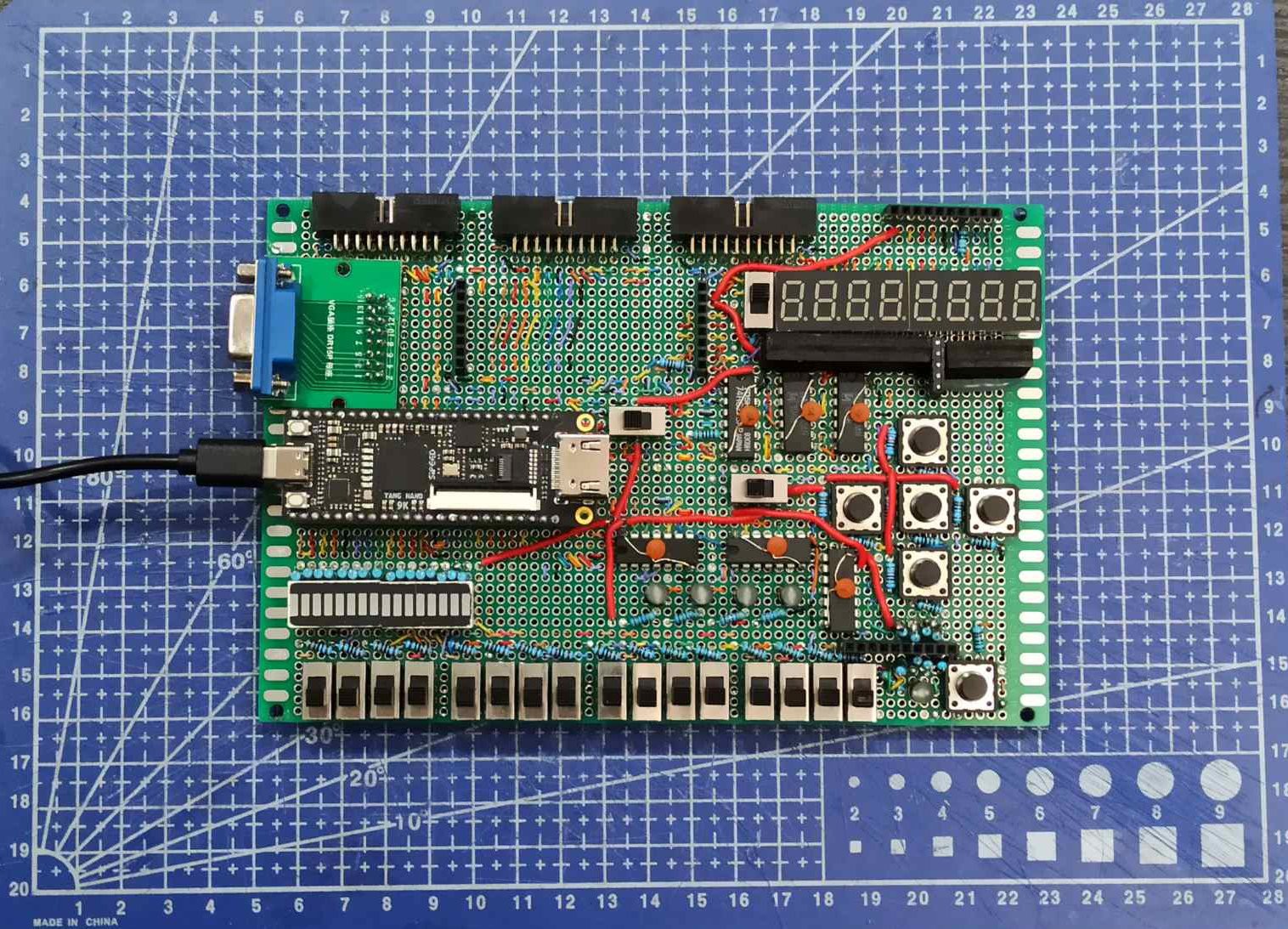
With 4 by 4 scan matrix keyboard:
![]()
----------
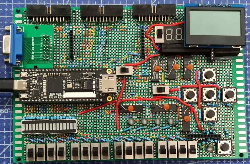
With 128*64px graphical LCD:
![]()
----------
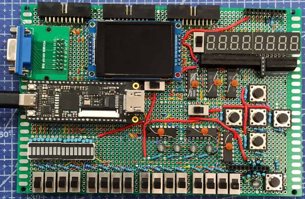
With 320*240px color LCD:
![]()
----------
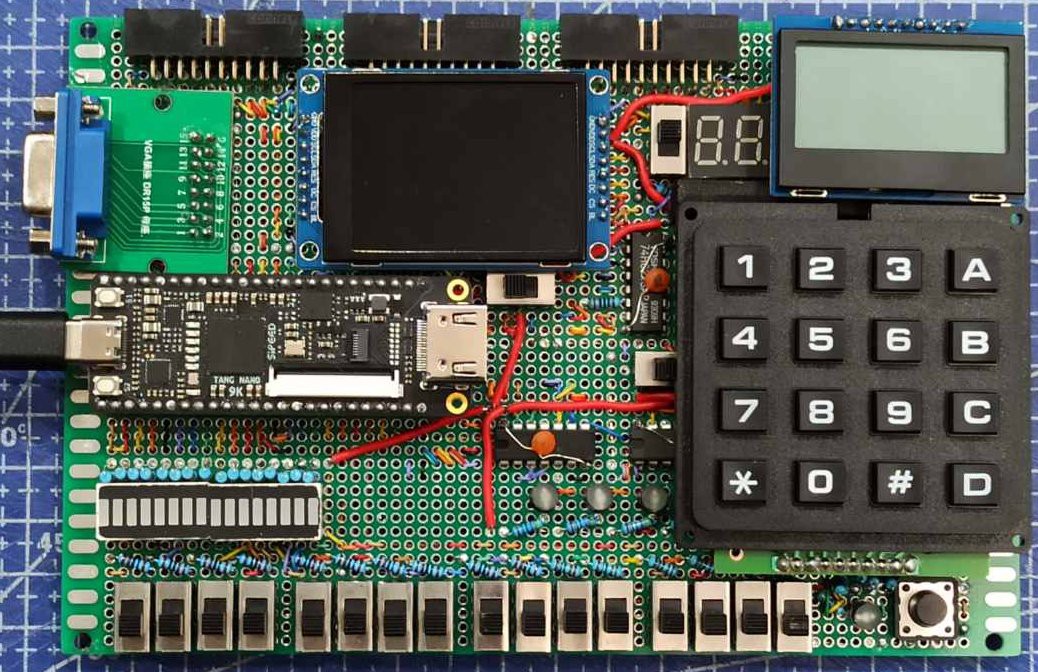
And, to top it all, the board with all extensions installed:
![]()
In this maximal configuration it is possible for each addon, as well as bottom row of switches and bottom-right button to work together. The lcd screens are connected via SPI protocol, and use the same wire for data transfer, but each have dedicated pin for selection, so can be multiplexed. With all of this, the VGA monitor also can be connected and show independent image, as signals for it are on dedicated pins from 1.8V bank.
-
The board is (almost) done
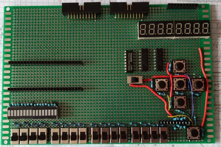
7 days ago • 0 commentsToday I finished primary soldering of all components on the board, and it looks like there is no bugs now.
The only thing I am planning to add here is one 74LVC245 chip in the spot under middle 20-pin connector, to be used as level shifter for 1.8V pins - to bring them up to 3.3V, thus on all 20-pin connectors all pins are 3.3V logic. But I do not have this chip yet, and haven't ordered it, so it will be deferred to future.
-----------------------
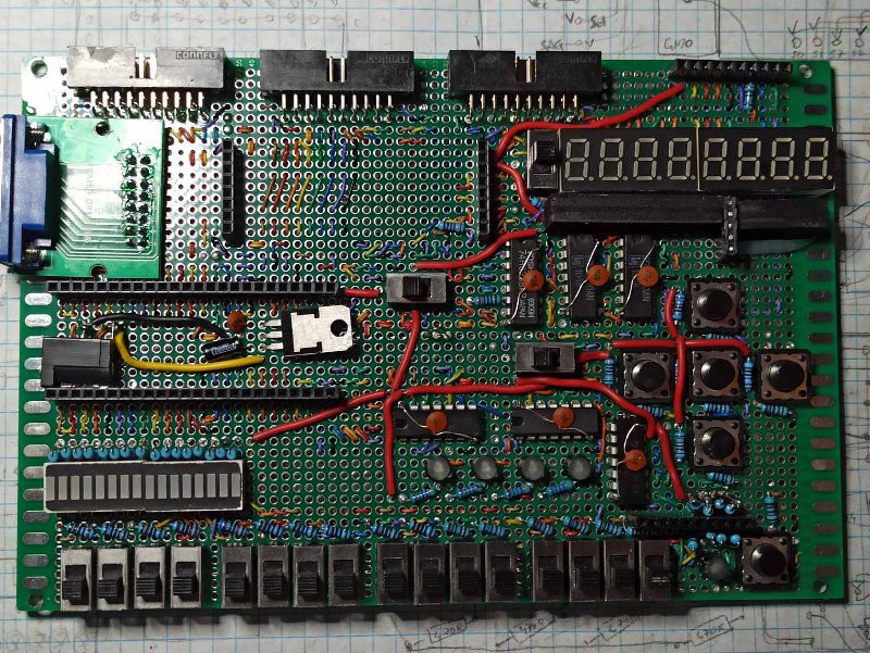
Here is how it looks like now,
front:
![]()
Going from top to bottom, left to right:
- The 3 20-pin connectors are on the top left and middle, they have all signal pins from Tang Nano 9k routed to them, as well as ground.
- Female pin header connector on the top right is the place for connecting small spi 128*64 graphical LCD.
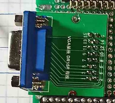
- VGA connector on the right, obviously to connect to VGA display.
- pair of female pin header connectors placed vertically with empty space between them is the place for connecting spi 320*240 TFT color display.
- to the right is multiplexed 8-digit 7-segment display, with switch that turns it off.
- pair of long female pin header connectors on the left of middle row is the socket for inserting the Tang Nano 9k FPGA board. The switch to the right of it disconnects the rest of the board from Vcc.
- on the right side, 5 push-buttons are set in cross arrangement.
- on the bottom, 16 switches are placed, and over them are LED banks which indicate switch positions. These could also be used as linear display, one just have to make sure all switches are off.
-- between LED banks and buttons are 4 circular LEDs that could be used as additional display (though it is tricky, as they are multiplexed with buttons).
- in the bottom right corner of the board is yet another push-button, with circular LED that indicates when it pressed.
- over this LED + button combo is femal pin header connector with is the attachment point of the 16-button keyboard.
--------------
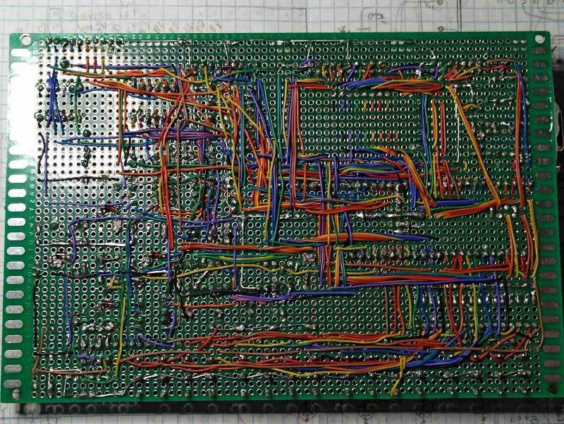
back:
![]() Most of the connections are routed on the back of the board by wire wrapping wire; the rest (mostly ground wires) are done by soldering component leads.
Most of the connections are routed on the back of the board by wire wrapping wire; the rest (mostly ground wires) are done by soldering component leads.
-------------------- -
Vandalizing the FPGA board
04/03/2026 at 07:35 • 0 commentsWhile testing the small 16-button keyboard, connected to the expansion board, I encountered a problem -- half of the buttons haven't registered keypresses at 10 kHz scan rate. When testing with manual scan - i.e. row address set statically through switches, all button presses where visible. After investigating with oscilloscope, I found out that some of the input pins on Tang Nano 9k board had too big capacitances attached, and charge/discharge of them was too long - it took almost a millisecond to reach proper logic level in my setup. This way, the shorter time period I used for scanning was not enough for proper voltage change and thus the registering button press.
Perusing board schematic I found out that several pins on board do indeed have capacitors attached -- those are dc filtering capacitors for hdmi signal lines. As I do not intend to use hdmi connector on this board, I decided that removing these capacitors will only be positive for my intended use -- and thus the surgery was performed:
![]()
The eight pairs of square pads in the middle are the connection points on smd capacitors that were used for filtering hdmi signal. They were interfering with inputs of shared GPIO pins (68 through 75), and were removed.
------------------------
Now, the board is not able to output hdmi signal, and in this way it is crippled. But, as I've mentioned above, I do not need hdmi output, and the capacitances were annoingly interfering with inputs, so for me now it is a net positive.
If in the future I should need the hdmi signal, I will have to generate it with other means, or order new untouched board.
-
Finalizing board design
03/20/2026 at 19:59 • 0 commentsI had started to put together and solder the board, while still designing layout -- this proved mutually beneficial process, as partially assembled board is very good anchor to further design, and having the design slightly ahead of implementation makes adding features a more thoughtful process.
In the process I came to think that there probably will be no 3.3V to 5V logic level conversion on this board (this might be done on separate board that will have to be connected to this one). Also I decided to make VGA output colors RGB222, as RGB332 has trouble with gray color. This decision releases two 3.3V GPIO pins that could be used elsewhere, as Hsync and Vsync signals are also routed to 1.8V bank.
On the other hand, I added connectors for add-on 16-button keyboard (that will block 5 buttons, and be used instead), and for 2 small spi LCD screens, one 128*64 dot matrix display, and other is 320*240 TFT display. They will use the same pins as multiplexed 7 segment display, so, mutually exclusive with it.
---------------------------------------
Here is partially assembled board:![]()
The switches and buttons are already installed and wired, and 7-segment displays are also wired together as multiplexed 8-digit display. The pin header connectors (female) are now soldered by just a couple points each, and still have no wiring connected.
---------------------------------------
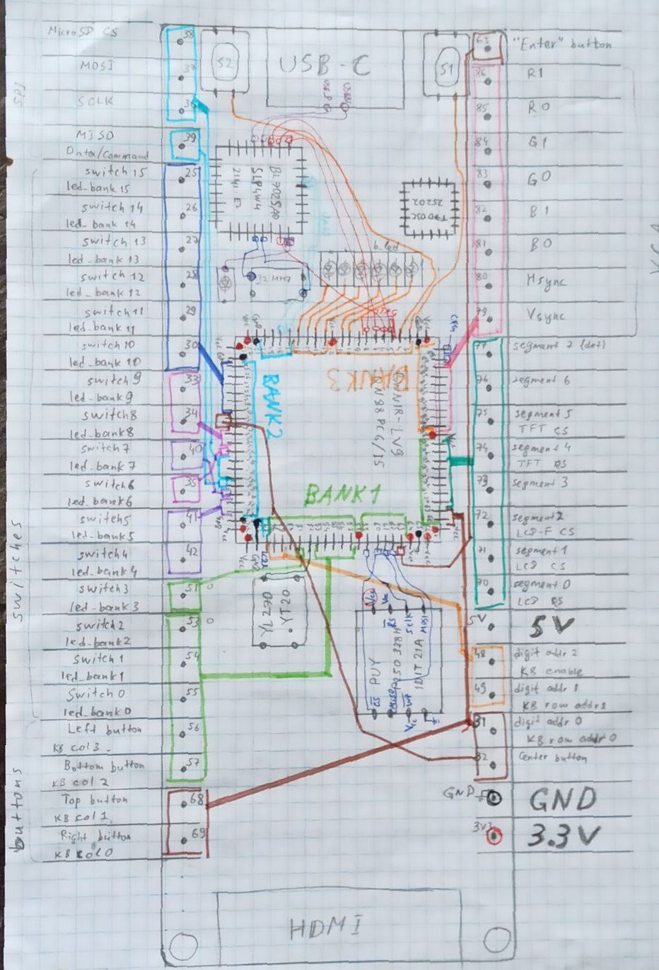
Here is provisional/draft design drawing:
![]()
---------------------------------------
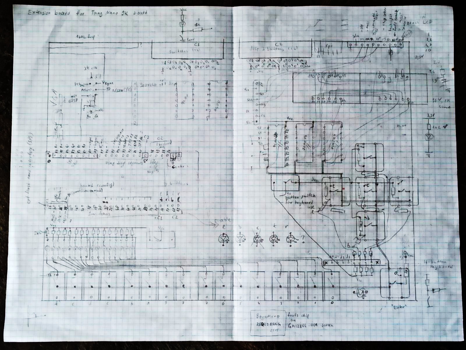
Pin assignments diagram:
![]() As one can see, on this diagram connections between main fpga IC and board connectors or other devices are traced. This is mostly for more intuitive look-up for writing appropriate .cst files needed for synthesis of Verilog descriptions.
As one can see, on this diagram connections between main fpga IC and board connectors or other devices are traced. This is mostly for more intuitive look-up for writing appropriate .cst files needed for synthesis of Verilog descriptions. -
Prototype update
03/07/2026 at 08:14 • 0 commentsThis is small update involving increasing the number of 7-segment displays available.
By adding an 3-to-8 decoder and inverters, it is possible to make an 8-character multiplexed segment, and at the same time use one less pin on the FPGA board.
The update is mostly cosmetic, but it also somewhat useful for showing internal states, and just to have directly controllable and simple display.
![]()
-
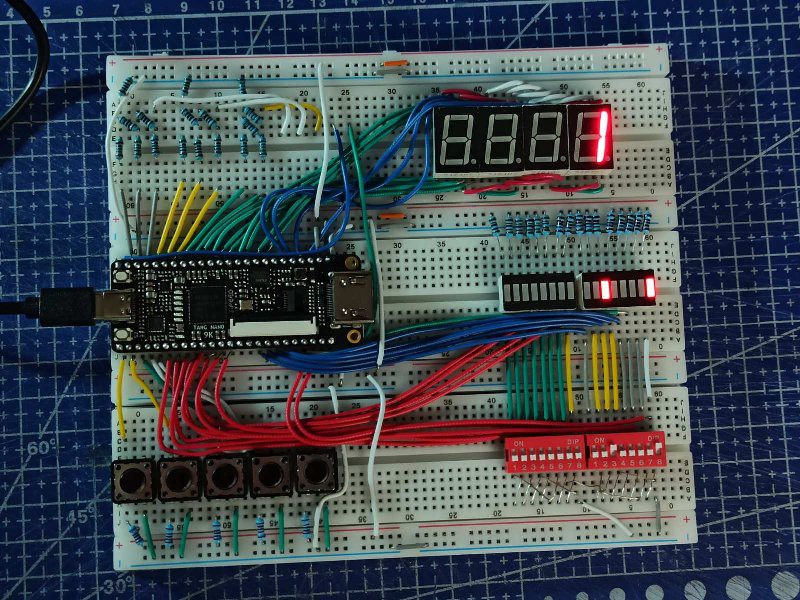
First prototype on breadboards
02/19/2026 at 19:02 • 0 commentsTo see, how it could look like, and to start using it already before permanent version is soldered, I made a prototype on breadboards -- it has 5 buttons and two 8-bit switch banks as inputs, as well as 4 7-segment displays wired for multiplexed use and 3,3,2 DAC for VGA output with RGB 332 color palette.
I did some testing with first primitive designs, and it seem to work ok.
![]() There are 8 1.8V IO pins, and all other IO is 3.3V logic. For my purposes 1.8V is too low voltage, and there seem to be little utility for these pins. The only thing I plan to interface this board with that has even lower working voltages is VGA interface. Thus these pins are to be used solely as outputs for VGA signal. On the prototype on photo they all connected to resistor network that forms 3 DACs (3, 3 and 2 bits, for R, G and B signals to be fed into VGA) in the top left corner.
There are 8 1.8V IO pins, and all other IO is 3.3V logic. For my purposes 1.8V is too low voltage, and there seem to be little utility for these pins. The only thing I plan to interface this board with that has even lower working voltages is VGA interface. Thus these pins are to be used solely as outputs for VGA signal. On the prototype on photo they all connected to resistor network that forms 3 DACs (3, 3 and 2 bits, for R, G and B signals to be fed into VGA) in the top left corner.
All the other IO pins on the top side of the board are connected to 4 7-segment displays configured to be driven as multiplexed 4-digit display (similar to what I once did with discrete components).
On the bottom side there are 5 buttons connected, as well as 16 switches (for now 2 DIP switch banks). Switches are also paired with LED banks, so that there is correspondence between each switch an LED - one can see which switches are ON right away. These same pins connected to switches as inputs can be configured as outputs -- the LEDs will act as display; for them to work properly in this way, all switches should be in OFF state.
Evaluation board shield for Tang Nano 9k FPGA
The extension board with switches, buttons, leds, VGA output and general interfaces.


 Most of the connections are routed on the back of the board by wire wrapping wire; the rest (mostly ground wires) are done by soldering component leads.
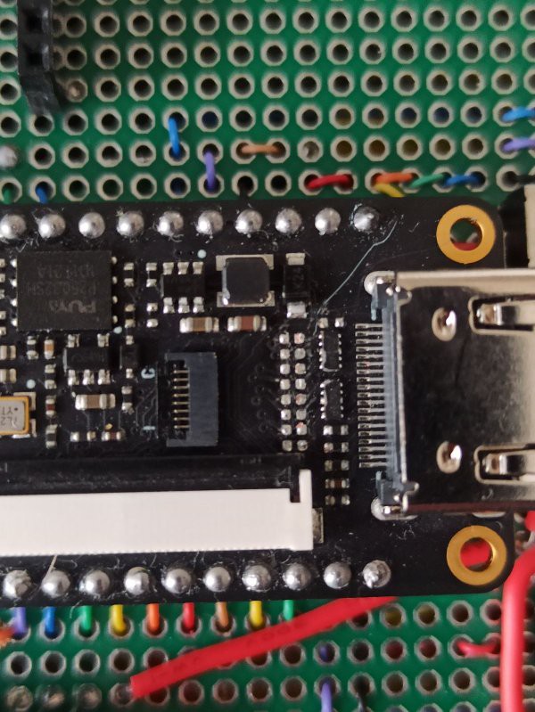
 As one can see, on this diagram connections between main fpga IC and board connectors or other devices are traced. This is mostly for more intuitive look-up for writing appropriate .cst files needed for synthesis of Verilog descriptions.
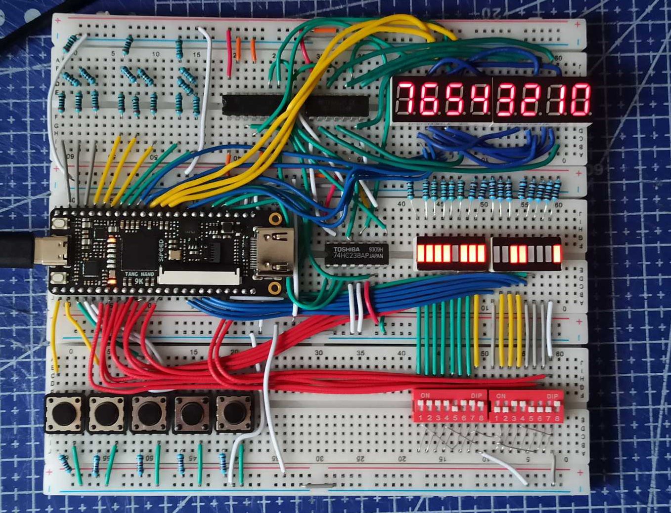
 There are 8 1.8V IO pins, and all other IO is 3.3V logic. For my purposes 1.8V is too low voltage, and there seem to be little utility for these pins. The only thing I plan to interface this board with that has even lower working voltages is VGA interface. Thus these pins are to be used solely as outputs for VGA signal. On the prototype on photo they all connected to resistor network that forms 3 DACs (3, 3 and 2 bits, for R, G and B signals to be fed into VGA) in the top left corner.