Z80 and 8052 SBC on DIP40 size MAX10 FPGA
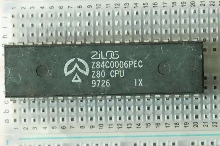
Zilog Z80 SBC with Z80 CPU, 8kB ROM, 8kB RAM and UART all implemented inside the FPGA and running BASIC Ver 4.7b.
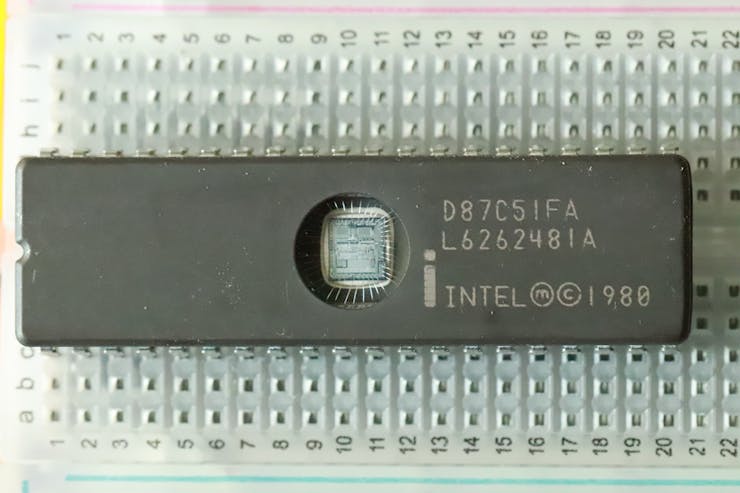
Intel 8052 SBC with 8052 CPU, 8kB ROM and 32kB RAM running BASIC-52 on a DIP40 size FPGA board running BASIC-52 at 50 MHz.
HISTORY:
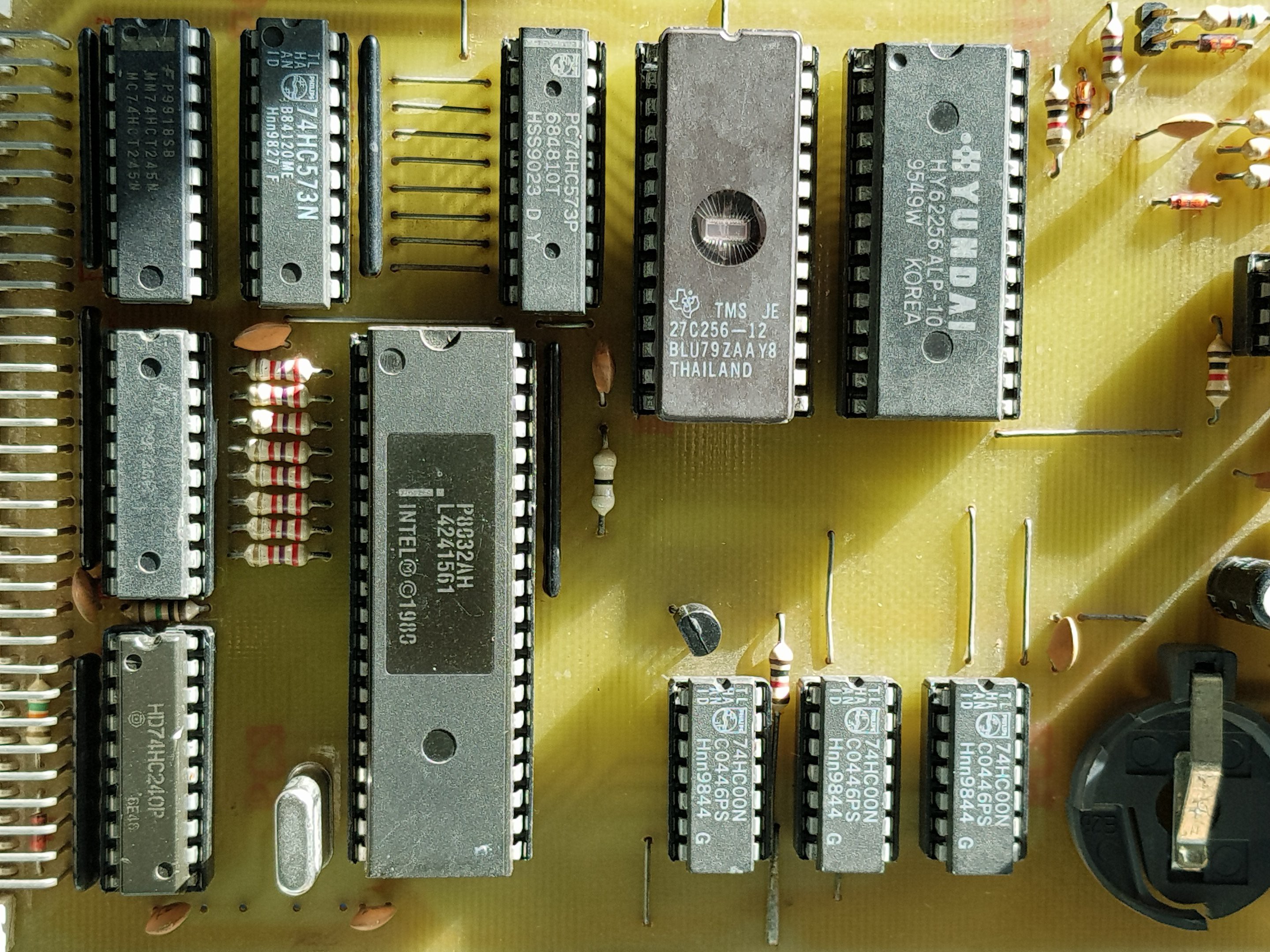
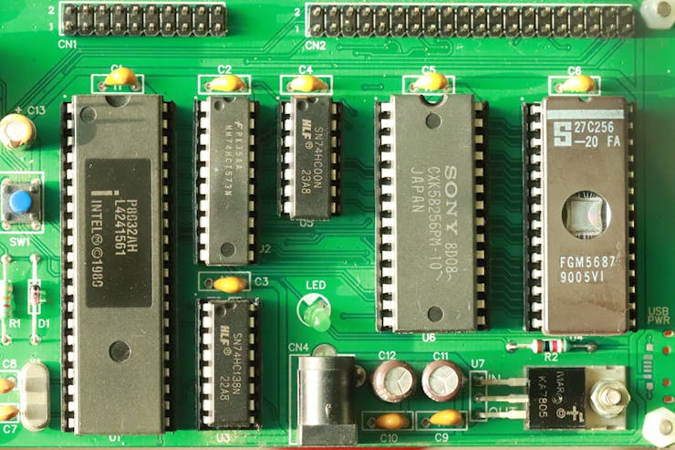
In the past, Conventional Classic Single Board Computer(SBC) will have a CPU, external ROM or EPROM, external RAM, latch, address decoder, I/O port, Reset circuit and crystal. The above board can be run with 8031 or 8032 controller. We can find more details HERE. The board comes with expansion board with which we can run FORTH.
The next generation SBC comes with processor with internal EPROM or FLASH memory which saved some board space and cost. More details about the below board can be found HERE.
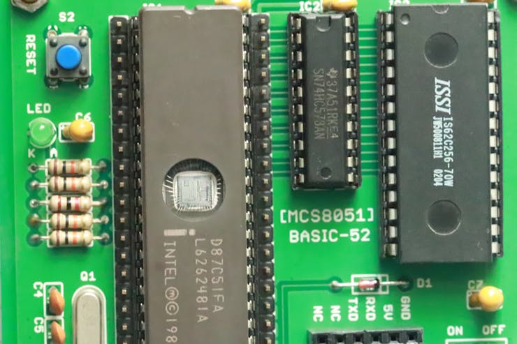
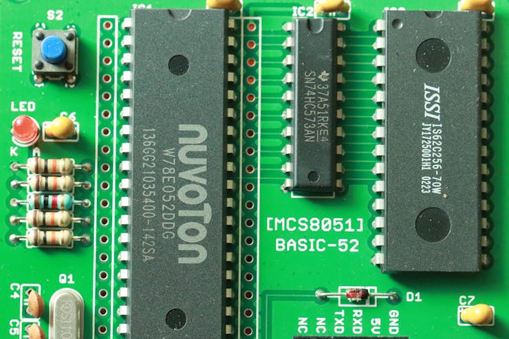
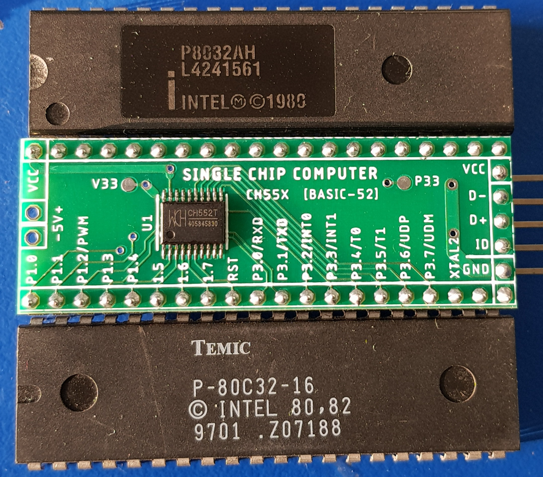
with the advance in technology, now we can implement the CPU, ROM, RAM, I/O port, UART all inside the programmable logic device using Hardware Description Language(HDL). The commonly used HDL are VHDL, Verilog and SystemVerilog.
SCOPE:
The scope of the project is to implement a Zilog Z80 based SBC with 8kB ROM and 8kB RAM running Microsoft BASIC Ver 4.7b and a Intel MCS-51 based SBC with 8kB code ROM and 32kB RAM running BASIC-52 with I2C extensions. It is same as the picture shown above which is having 8kB ROM and 32kB RAM.
FPGA:
The main goal is to implement the whole SBC on a DIP-40 size form factor board. After some search the target device narrowed down to Altera FPGA MAX 10 family device.
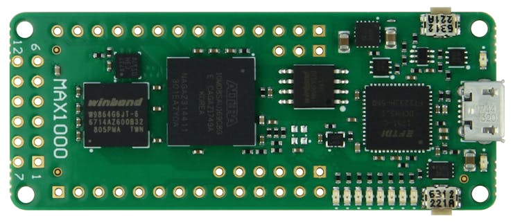
This board is a small size board with lots of resource and low in cost. The formfactor is not exactly DIP-40 size and the board contains more resources than we need. The FPGA used is MAX10 family 10M08SAU169C8G. We can learn more about the MAX1000 board HERE.
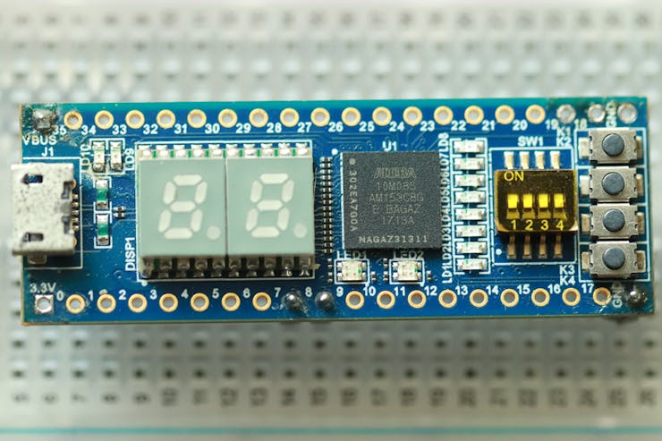
The above board also comes with MAX10 FPGA and having exact DIP-40 size. We can find Hardware, Software and Example project HERE. We can also find the overview for the above board at HERE.
The MAX10 FPGA devices are new generation devices which having combination of CPLD and FPGA architecture. The MAX10 devices comes with internal FLASH memory so that we do not require external configuration device during power-up. The MAX10 devices also comes with inbuilt ADC and temperature sensor.
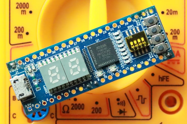
We just need 4 connections for simple SBC operation for both Zilog Z80 or Intel MCS-51 based SBC. In both Z80 and MCS-51, the I/O PORT1 is mapped to the 8 onboard LEDs. The SBC reset is assigned to the K1 button.

Zilog Z80 SBC on MAX10 FPGA:
For a minimal Z80 SBC running Microsoft BASIC Ver 4.7b, we need 8kB ROM space and 4kB RAM space. We will implement 8kB RAM in this system. There are still lots of Logic Elements and Memory Bits available which is useful for future expansion.
The SBC system was compiled and tested using Quartus II 18.1 version. Just open the Quartus II and restore the archive file.
The project folder also contains the SRAM Object File(SOF) and Programmable Object File(POF) ready to use without compiling.
Connect the Micro USB cable to the MAX10 board and program the SOF or POF file. SOF will lost after power cycle. POF will be stored inside the FLASH and comes alive for every power ON.
The below code in BASIC just counts from 0 to 255 on Z80 SBC I/O...
Read more » mit41301