
 mit41301
-
SN76489 programmable sound generator
06/26/2026 at 07:32 • 0 commentsSN76489 programmable sound generator using VHDL and CPP
![]()
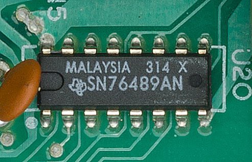
SN76489-DIP16 ![]()
![]()
Texas Instruments SN76489 - Wikipedia
SN76489 Complex Sound Generator
VHDL, BSD 3-Clause
A huge amount of effort has gone into making this core as accurate as possible to the real IC, while at the same time making it usable in all digital SoC designs, i.e. retro-computer and game systems, etc. Design elements from the real IC were used and implemented when possible, with any work-around or changes noted along with the reasons.
Synthesized and FPGA proven:
- Xilinx Spartan-6 LX16, SoC 21.477MHz system clock, 3.58MHz clock-enable.
References:
- The SN76489 datasheet
- Insight gained from the AY-3-8910/YM-2149 die-shot and reverse-engineered schematics (similar audio chips from the same era).
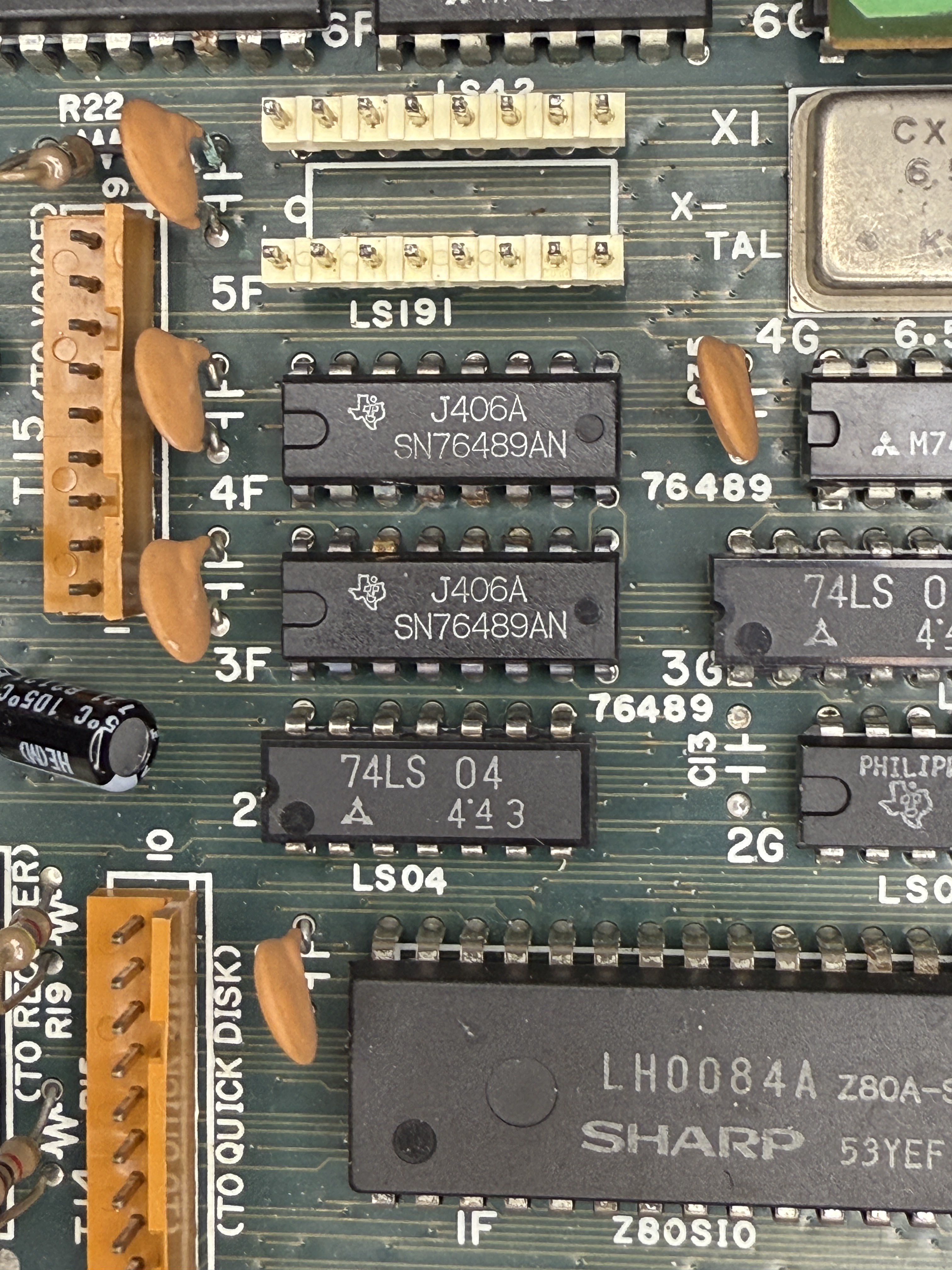
- Real hardware (SN76489 in a ColecoVision game console).
- Chip quirks, use, and abuse details from friends and retro enthusiasts.
Generates:
- Unsigned 12-bit output for each channel.
- Unsigned 14-bit summation of the four channels.
- Signed 14-bit PCM summation of the four channels, with each channel converted to -/+ zero-centered level or -/+ full-range level.
The tone counters are period-limited to prevent the very high frequency outputs that the original IC is capable of producing. Frequencies above 20KHz cause problems in all-digital systems with sampling rates around 44.1KHz to 48KHz. The primary use of these high frequencies was as a carrier for amplitude modulated (AM) audio. The high frequency would be filtered out by external electronics, leaving only the low frequency audio.
When the tone counters are limited, the output square-wave is disabled, but the amplitude can still be changed, which allows the A.M. technique to still work in a digital Soc.
I/O requires at least two clock-enable cycles. This could be modified to operate faster, i.e. based on the input-clock directly. All inputs are registered at the system-clock rate.
Optionally simulates the original 32-clock (clock-enable) I/O cycle.
The SN76489 does not have an external reset and the original IC "wakes up" generating a tone. This implementation sets the default output level to full attenuation (silent output). If the original functionality is desired, modify the channel period and level register initial values.
Basic I/O interface use:
- Set-up data on data_i.
- Set ce_n_i and wr_n_i low.
- Observe ready_o and wait for it to become high.
- Set wr_n_i high, if done writing to the chip set ce_n_i high.
SN76489 Complex Sound Generator
TDSN76489
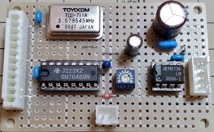
SN76489 implementation for Teensyduino Audio Library
Information regarding the implementation of the Sega Master System's variant of the SN76489 can be found at: http://www.smspower.org/Development/SN76489
Example sketches in this library use VGM files to test the SN76489. VGM files for Master System are commonly found in compressed format (7z) on the web. To use them with this libary you will need to extract them:
Linux users:
7za -e %vgmfile>#/p###
Afterwards, if you wish to generate a header file which can be included in a project:
xxd --include %extractedvgmfile% &> %file>#/p###
Windows users: ask google
TDSN76489
-
Backup OSCCAL
05/25/2026 at 14:04 • 0 commentsThis document includes the programming specifications for the following devices:
• PIC10F200
• PIC10F202
• PIC10F204
• PIC10F206MEMORY MAPPING
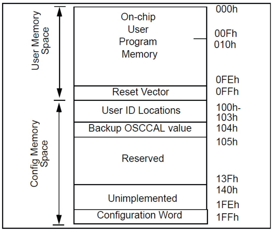
User Program Memory Map
The user memory space extends from (0x000-0x0FF) on the PIC10F200/204 and (0x000-0x1FF) on the PIC10F202/206. In Program/Verify mode, the program memory space extends from (0x000-0x1FF) for the PIC10F200/204 and (0x000-0x3FF) for the PIC10F202/206. The first half, (0x000-0x0FF) and (0x000-0x1FF) respectively, is user program memory. The second half, (0x100-0x1FF) and (0x200-0x3FF) respectively, is configuration memory. The PC will
increment from (0x000-0x0FF) and (0x000-0x1FF) respectively, then to 0x100 and 0x200, respectively (not to 0x000).
In the configuration memory space, 0x100-0x13F for the PIC10F200/204, and 0x200-0x23F for the PIC10F202/206, are physically implemented. However, only locations 0x100-0x103 and 0x200-0x203 are available. Other locations are reserved.![]()
PIC10F200/204 PROGRAM MEMORY MAP HOW TO VIEW THE BACKUP OSCCAL?
The memory locations 0x0100-0x103 are used for User ID Locations. The backup value of the OSCCAL value is located at 0x0104.
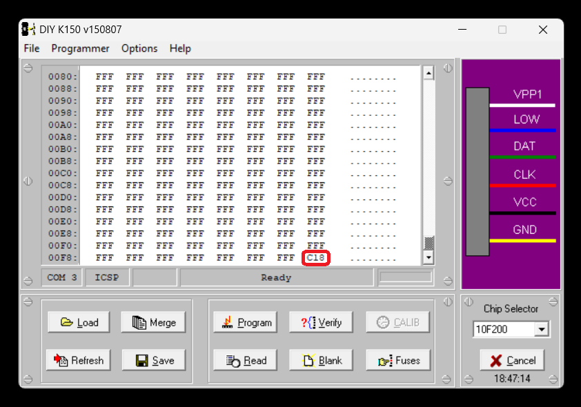
Take any fresh PIC10F200 and read the content normally.
![]()
We can see the final location of the FLASH memory contains the OSCCAL value of 0xC18
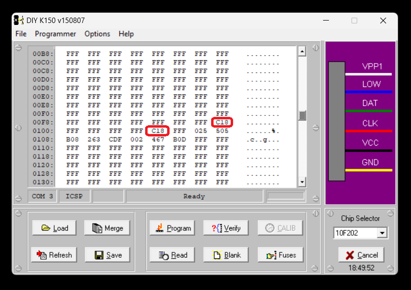
Now set the device as PIC10F202. By this way the programmer able to access the higher memory locations.
![]()
In the above view please note the selected chip is PIC10F202. But the actual chip we used is PIC10F200. At the memory location 0x0104 we can see the same OSCCAL value which in this chip is 0xC18.
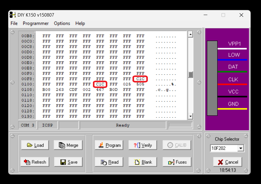
Below is the screen view for one more PIC10F200 chip
![]()
In the above case the different PIC10F200 which is having the OSCCAL of 0xC1C. The same value of 0xC1C can be seen at the location 0x0104.
Other values are RESERVED as per Microchip and needs further investigation.
-
BASIC-52 INSTRUCTION SET SUMMARY
03/07/2026 at 14:03 • 0 commentsCOMMANDS STATEMENTS OPERATORS RUN BAUD ADD (+) CONT CALL DIVIDE (/) LIST CLEAR EXPONENTIATION (**) LIST# CLEAR(S&I) MULTIPLY (*) LIST@ (V1.1) CLOCK(1&0) SUBTRACT (-) NEW DATA LOGICAL AND (.AND.) NULL READ LOGICAL OR (.OR.) RAM RESTORE LOGICAL X-OR (.XOR.) ROM DIM LOGICAL NOT (.OR.) XFER DO-WHILE ABS( ) PROG DO-UNTIL INT( ) PROG1 END SGN( ) PROG2 FOR-TO-STEP SQR( ) PROG3 (V1.1) NEXT RND PROG4 (V1.1) GOSUB LOG( ) PROG5 (V1.1) RETURN EXP( ) PROG6 (V1.1) GOTO SIN( ) FPROG ON-GOTO COS( ) FPROG1 ON-GOSUB TAN( ) FPROG2 IF-THEN-ELSE ATN( ) FPROG3 (V1.1) INPUT =, >, >=, <, <=, <> FPROG4 (V1.1) LET ASC( ) FPROG5 (V1.1) ONERR CHR( ) FPROG6 (V1.1) ONEX1 CBY( ) ONTIME DBY( ) PRINT XBY( ) PRINT# GET PRINT@ (V1.1) IE PH0. IP PH0.# PORT1 PH0.@ (V1.1) PCON PH1. RCAP2 PH1.# T2CON PH1.(@ (V1.1) TCON PGM (V1. 1 ) TMOD PUSH TIME POP TIMER0 PWM TIMER1 REM TIMER2 RETI XTAL STOP MTOP STRING LEN UI(1&0) FREE U0(1&0) PI LD@ (V1. 1 ) ST@ (V1. 1 ) IDLE (V1.1) RROM (V1. 1 )
My Projects
My Pages
Projects I Like & Follow
 Mitsuru Yamada
 Stephen
 CheeenNPP
 MS-BOSS
 Burkhard Kainka
 Rudraksha Vegad
 Kuba Sunderland-Ober
 Stephan Martin
 Jesse Farrell
 bornach
 Ted Sheflin
 CustomElectronics
Share this profile
ShareBits


Mitsuru Yamada
wrote 05/10/2023 at 01:35
•
point
Thank you for following my projects! I am committed to recreating basic digital computer technology and analog technology circa late 1970s.
Thank you for liking and following my #CMOS Homemade Operational Amplifier ! This project made me realize the characteristics of MOSFET semiconductors in my own way.