When starting the project, I had several requirements on my mind:
- Single supply operation, preferably in the range 9-12V.
- No trimming should be necessary to obtain reasonable accuracy.
- No "exotic" parts nor part values (especially resstors!) should be used.
- Possibly low current consumption of the circuit. (not met that well!)
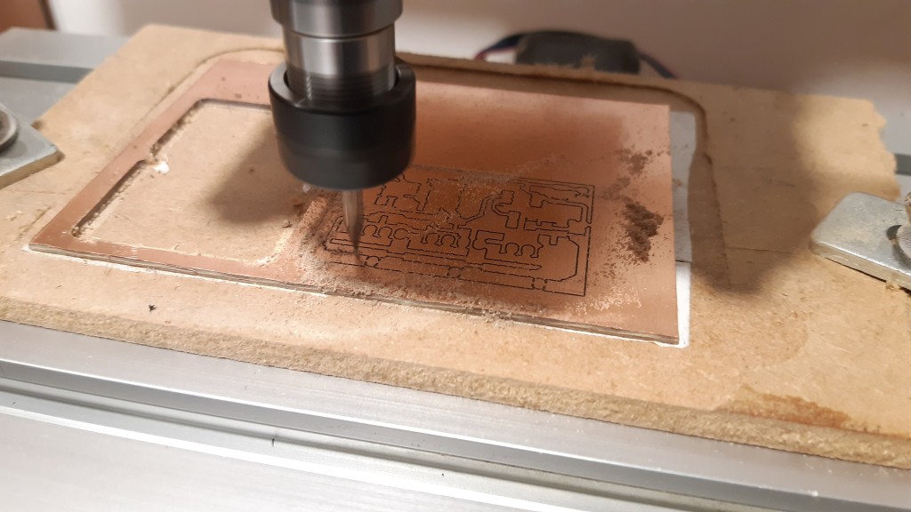
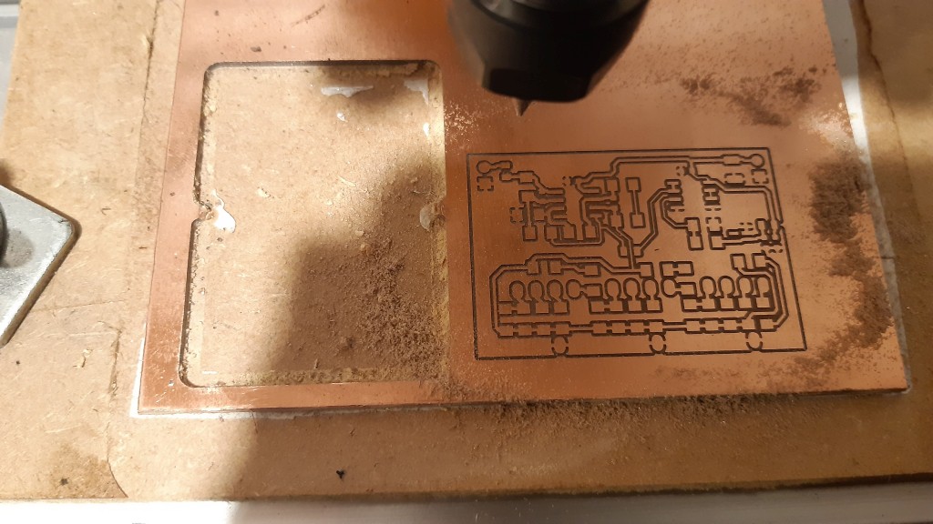
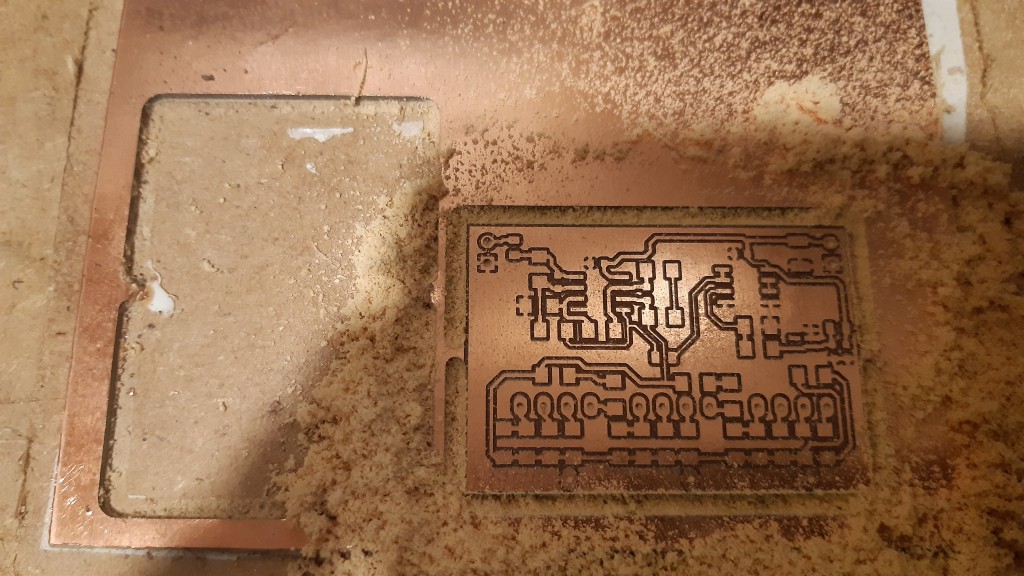
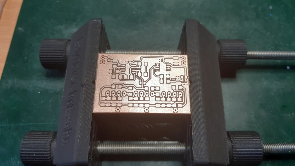
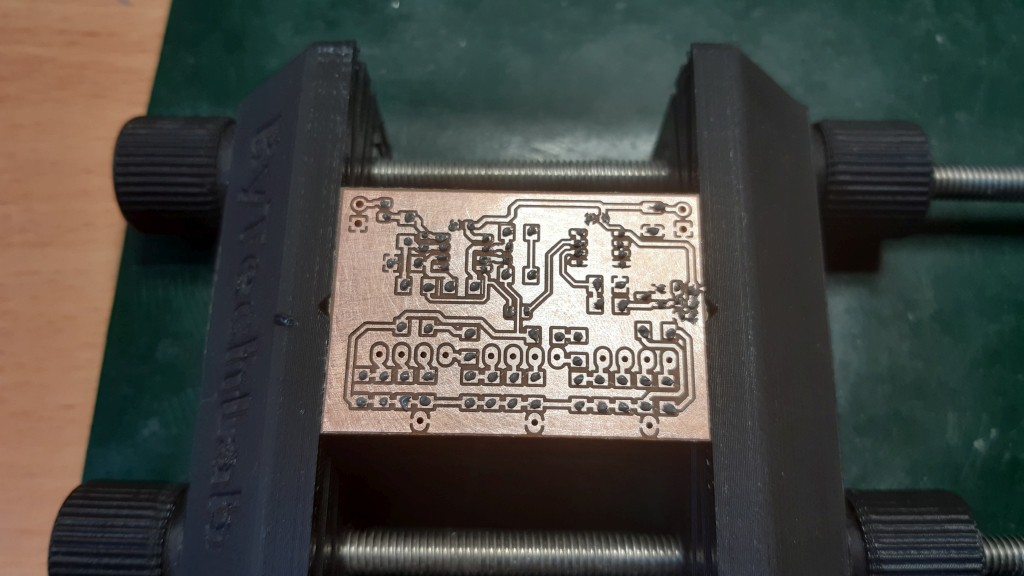
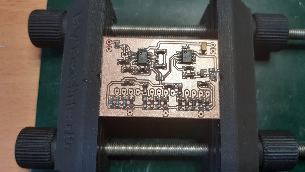
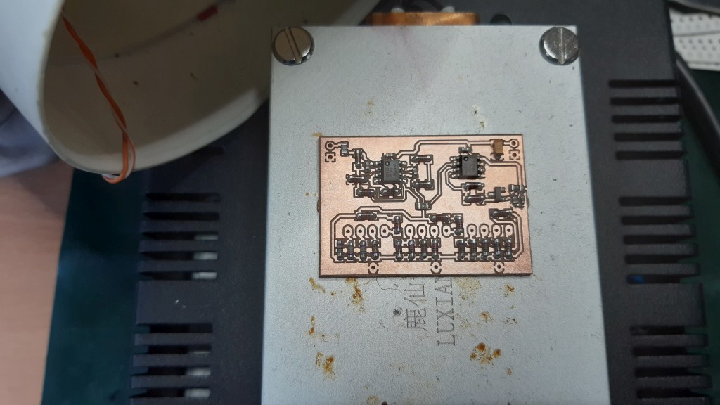
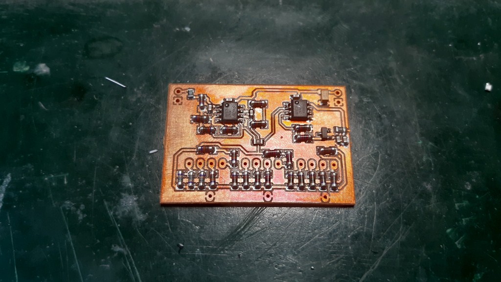
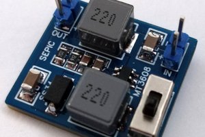
- Possibly a single sided board that can be produced by a simple "Chinese" CNC mill.
The circuit I used is shown below:
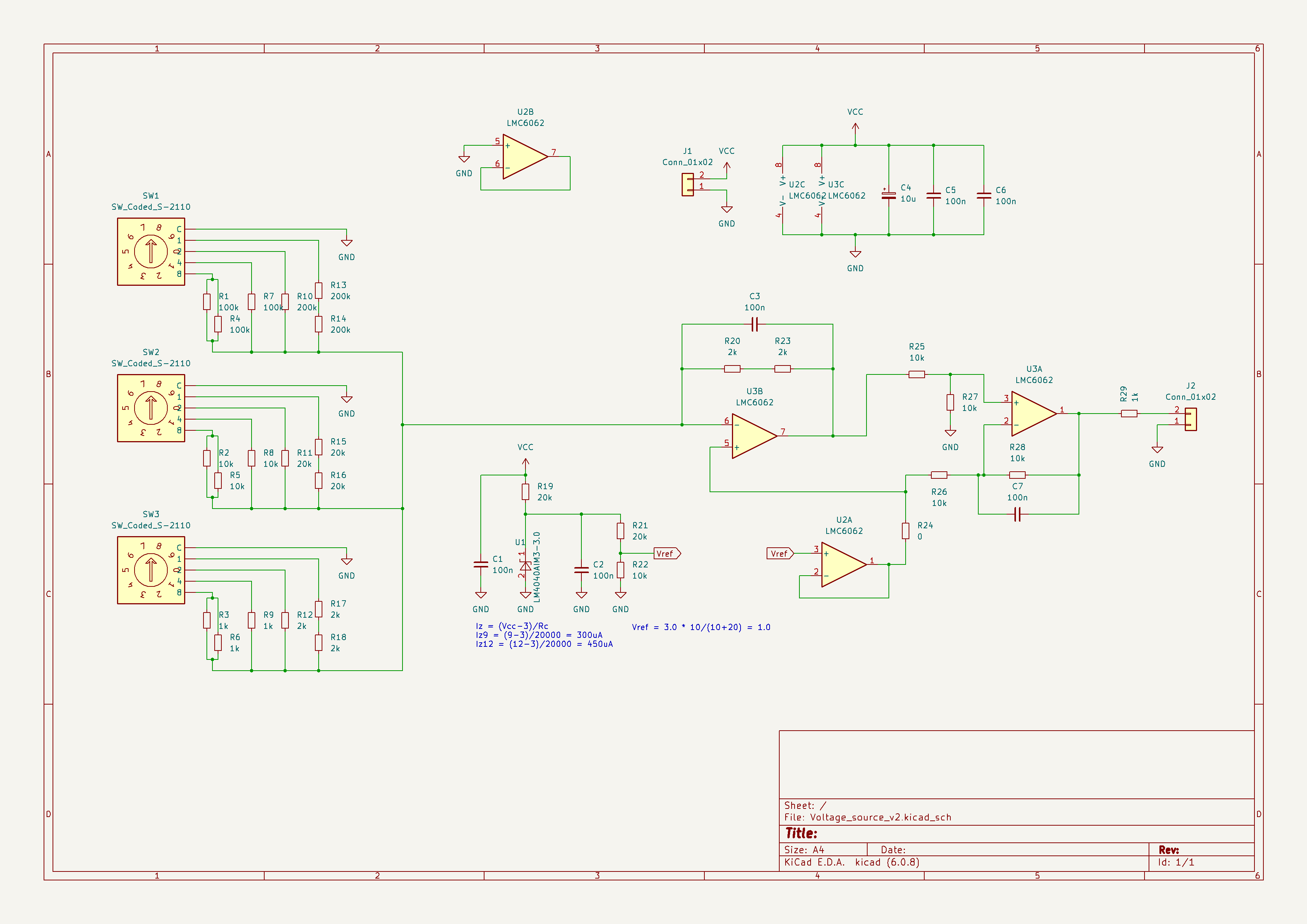
Details of the circuit
Reference voltage source
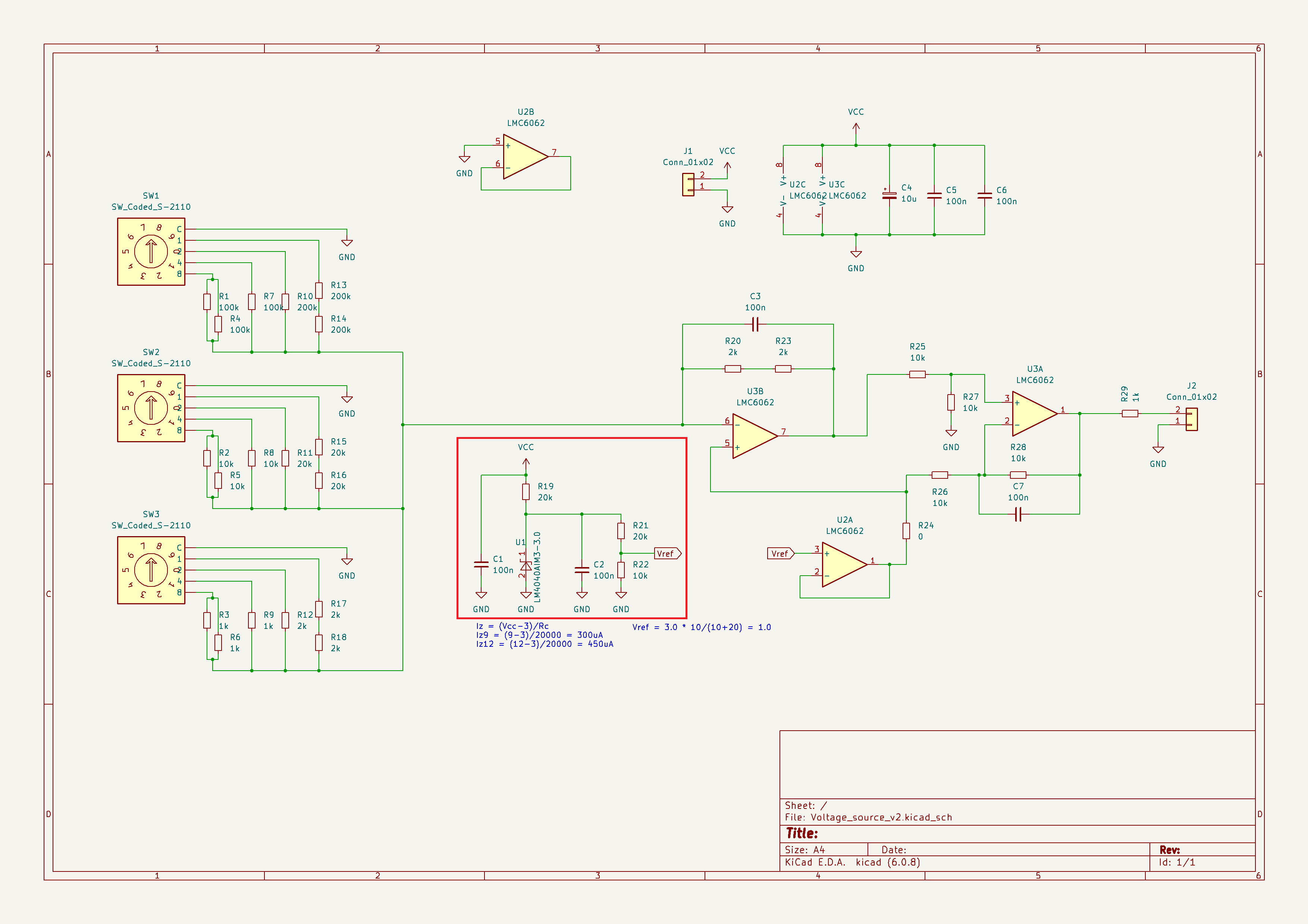
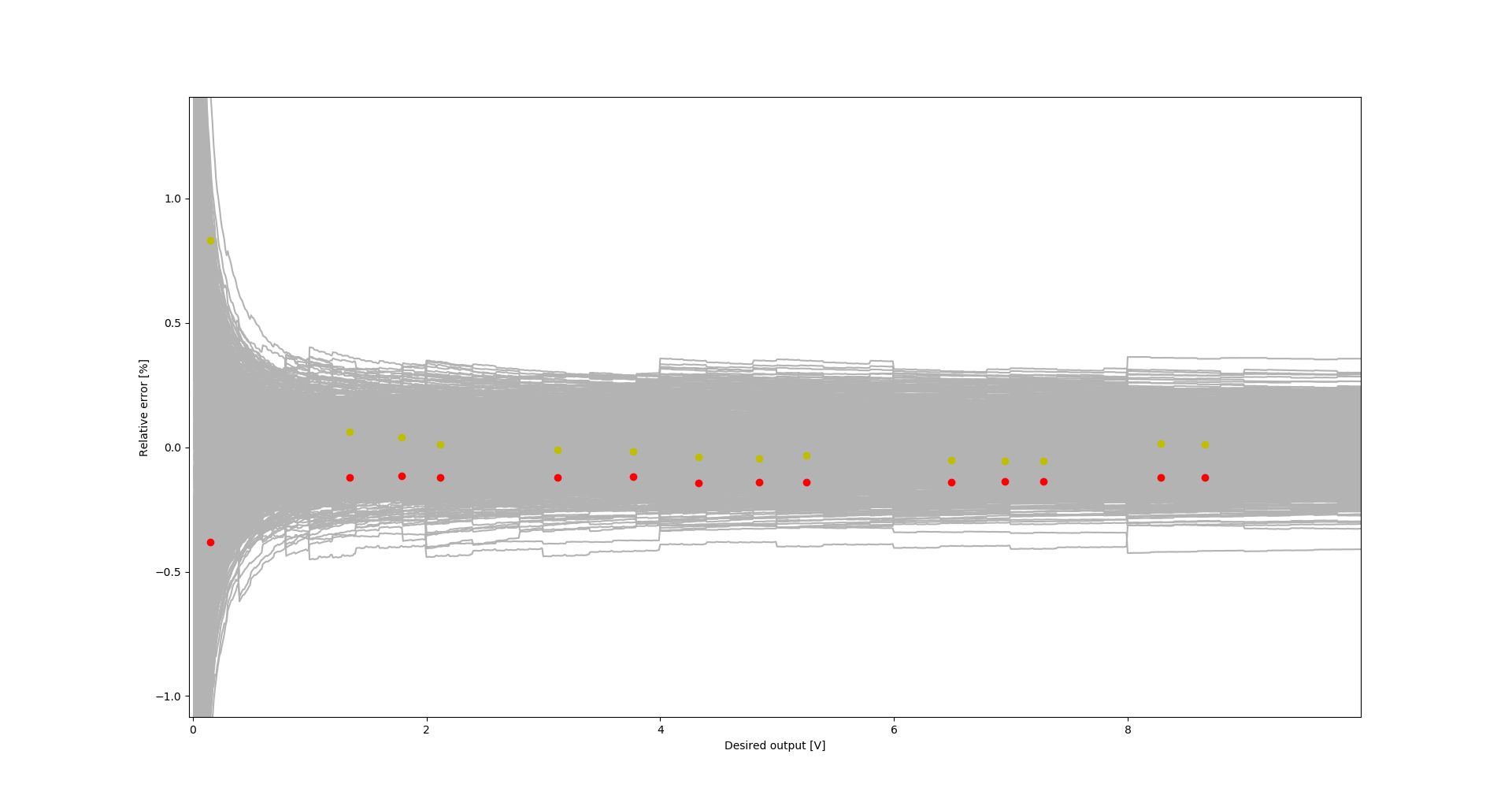
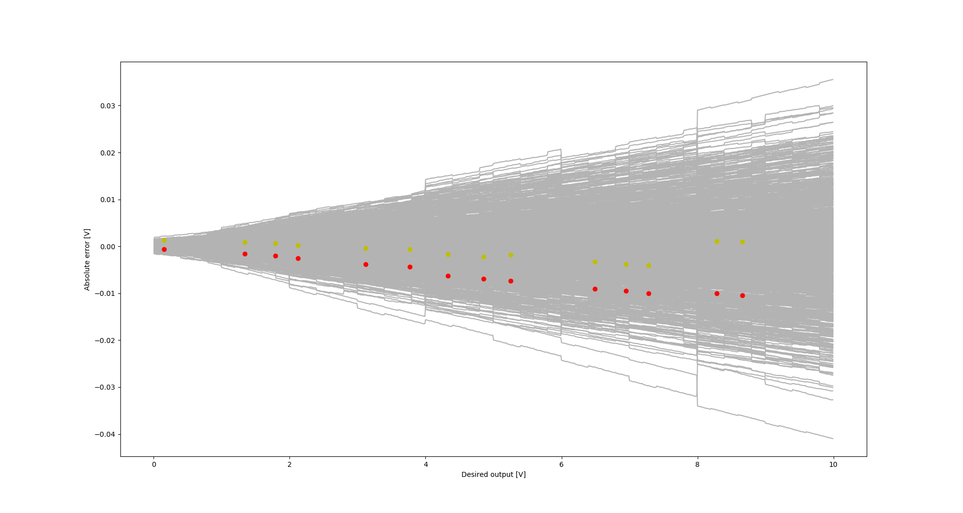
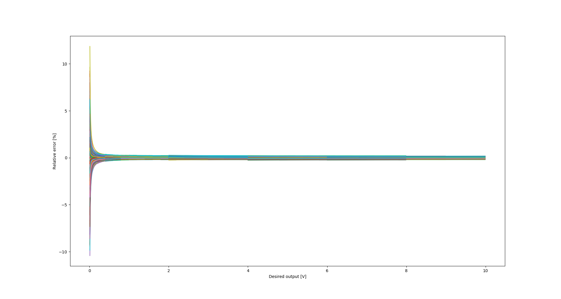
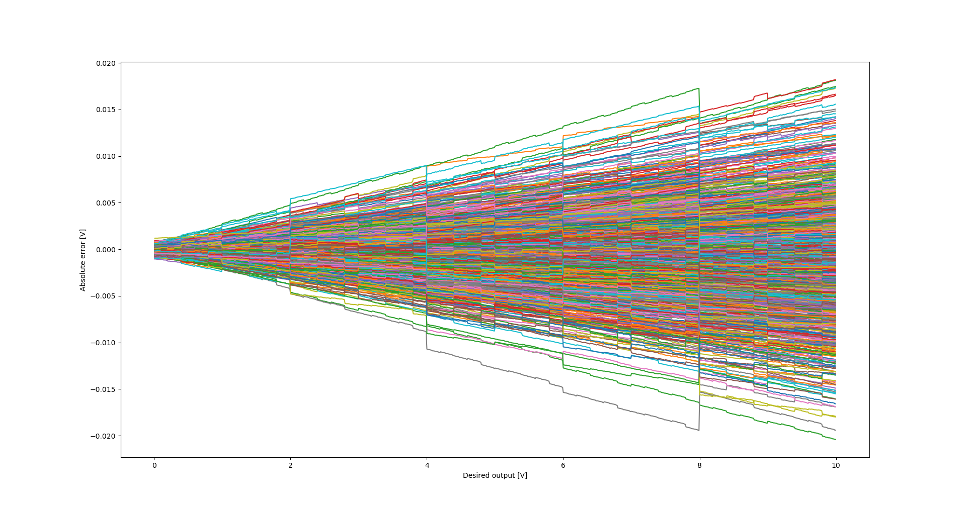
The principle of operation of the circuit starts with a stable and accurate reference voltage. I needed this to be 1V to make the simple setting of output voltage possible. In fact, any integer value of the reference voltage would do, but 1V seemed to be easy to obtain and required no "difficult" resistor values.
To produce the 1V reference voltage without using any trimmers, the LM4040A circuit is chosen. The A version may be more expensive (approximately twice the cost), but provides better accuracy. This accuracy would be degraded by further processing steps, so it is good to start with better accuracy.
LM4040 has a version that produces 3V on the output and it seems to be widely available. To produce 1V, the output voltage has to be divided in ratio 1/3, and that requires a resistor divider with values R + 2R. Luckily, values like 1k and 2k, 10k and 20k are easily available, so this was the way to go. I used precise 0.1% resistors R21 and R22 in the divider. The value of R19 does not need to be precise - a 1% or even 5% resistor should do. The value of R19 (20k) is chosen so that a sufficient current is provided for LM4040 to function properly. For the assumed supply voltage range 9 to 12V, the LM4040 current will be in the range from 300 to 450uA, that is enough to maintain the proper operation of LM4040.
Reference voltage buffer
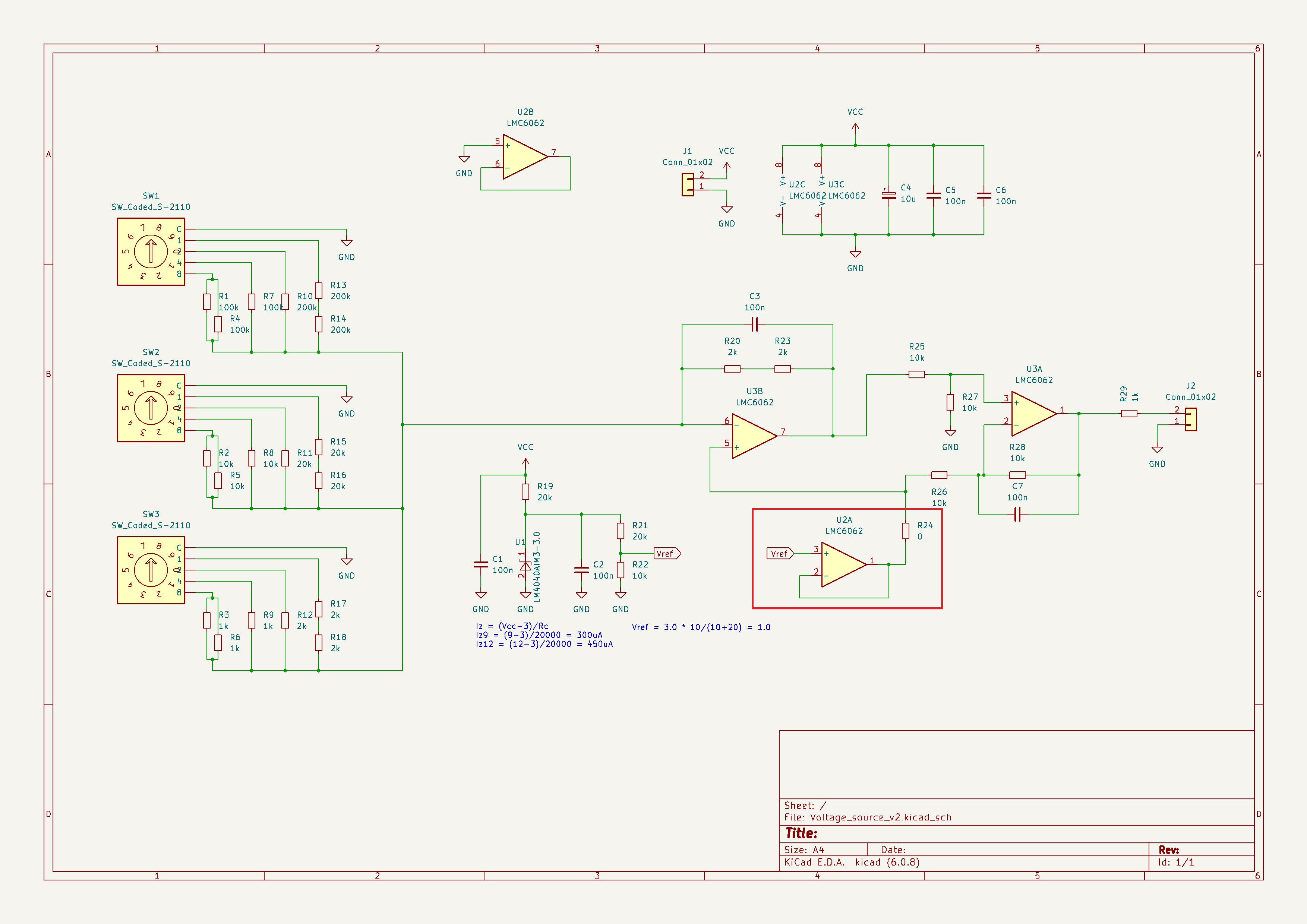
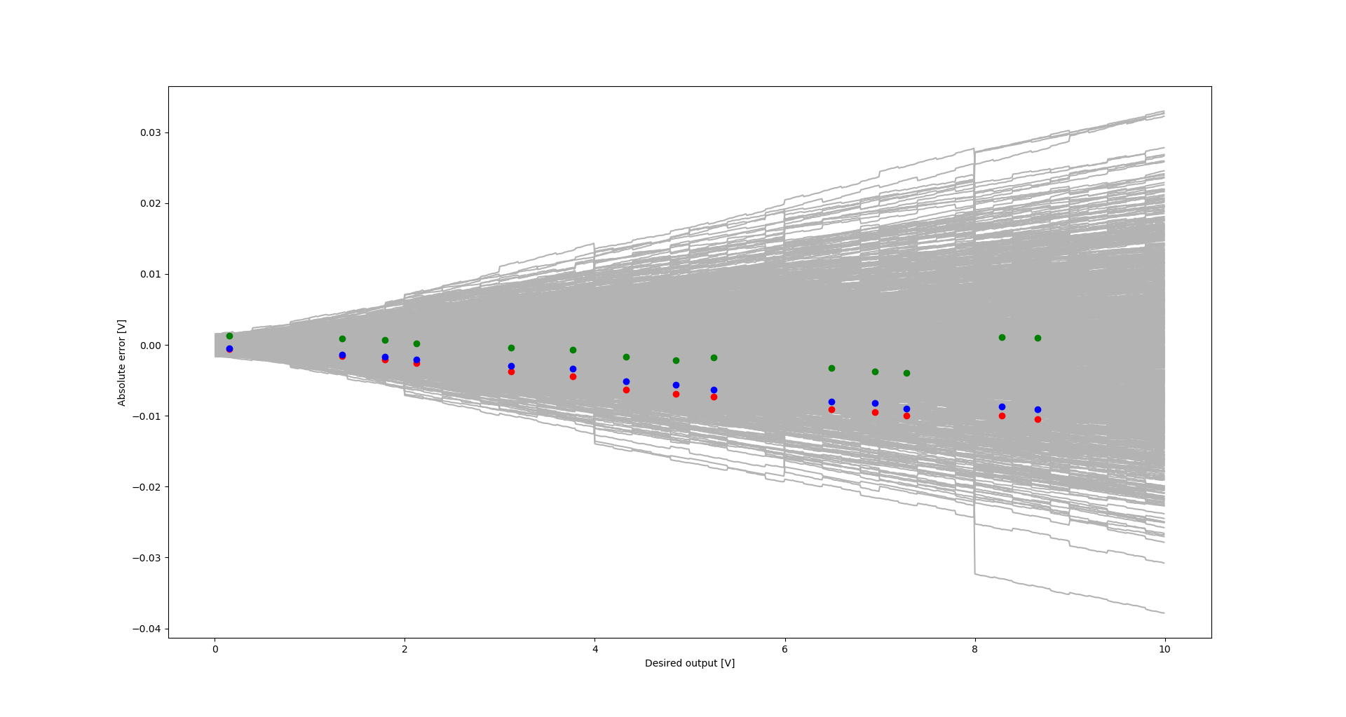
Since the 1V reference voltage is present on the output of a voltage divider with significant output resistance (6.67k), I use a voltage buffer to provide low output resistance of the 1V reference voltage. Decreasing this resistance proved to be essential for accurate operation of the remaining part of the circuit. Using lower resistance values in the voltage divider would not help, since to get a very low output resistance, in the order of 1 Ohm or less, would require the use of prohibitively low values of resistors and increase the voltage divider current to about 300mA.
Another aspect that needs considering is the choice of the operational amplifier. It needs to have a set of properties:
- low input bias current (in order not to introduce significant errors caused by loading of the voltage divider)
- low input offset voltage (in order not to introduce significant errors to the output voltage)
- rail to rail on input and output operation (in order to be able to work with a single supply voltage and provide wide range of output voltage)
I chose LMC6062 because I can easily get them for a reasonable price. They are precision (=low offset voltage) CMOS (=low bias current) amplifiers. The specified supply voltage is from 4.5V up to 15V. Especially the second value is important - many modern opamps do not work with supply voltage above 5.5V. LMC6062 is also a rail to rail opamp, which is important in this project. They also have quite high typical open loop voltage gain, that helps to maintain consistiency between real life performance and results of simple calculations we are used to. Plus, there are two of them in a single SO8 package.
Resistor R24 is there only to help in routing the tracks on the PCB and its value is 0 Ohms.
Voltage generator
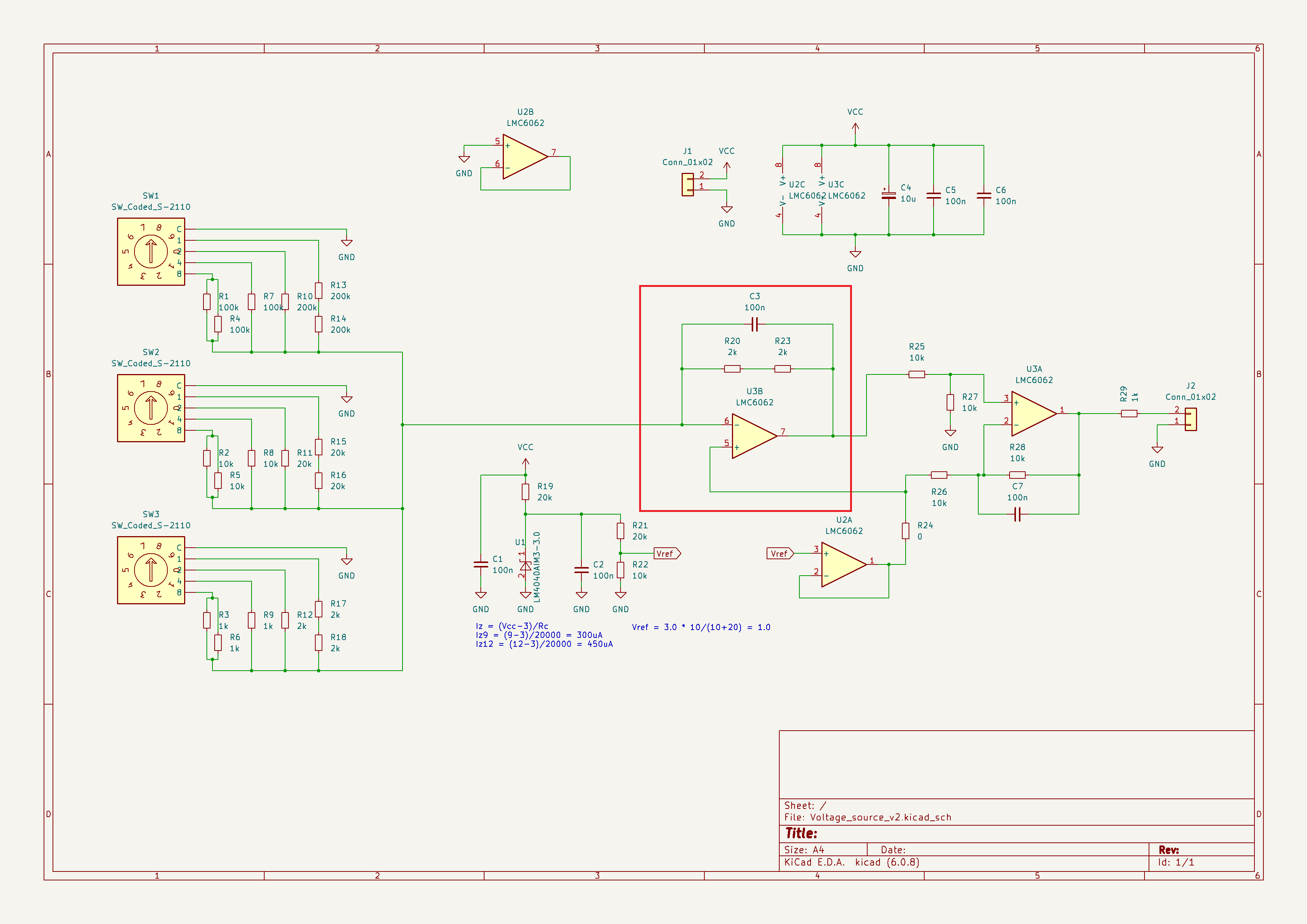
This is the part of the circuit where the desired voltage is generated.
The way it works is the following.
The voltage on the non-inverting input (pin...
Read more »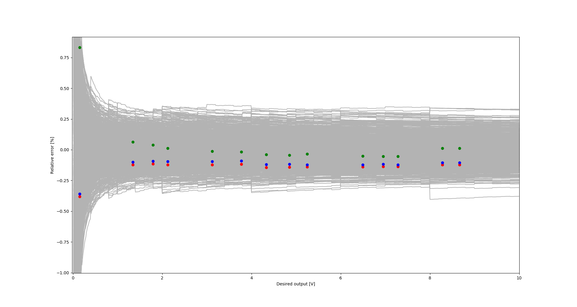

 Stefan Wagner
 w_k_fay
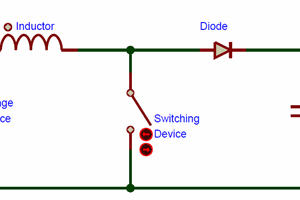

 mircemk
The layout with the MELF resistors is mesmerizing. The single layer is a nice challenge.