 dylan zheng
-
1Jumperlink Manual
![]()
1. Introduction
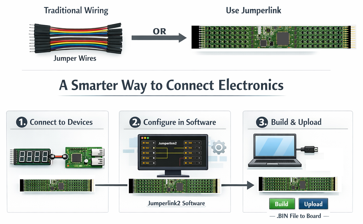
Jumperlink is a smart electronic connection platform designed to simplify circuit prototyping and testing. It replaces traditional jumper wires by allowing users to create electrical connections through software control, making circuit setup faster, cleaner, and more flexible.
Instead of manually wiring connections on a breadboard, Jumperlink uses an internal switching matrix to route signals between pins. This enables rapid reconfiguration of circuits without physically changing wiring, reducing setup time and minimizing human error.
By removing the need for physical jumper wires, Jumperlink helps streamline workflows, improve reliability, and create a more efficient development environment for engineers, students, and makers.
2. Logical diagram
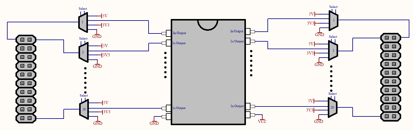
Jumperlink is built around a central FPGA and features 20 pins on each side of the board in a symmetrical layout.
Its logical diagram is shown below:
![]()
Each pin is routed through a multiplexer positioned between the FPGA and the external connector. This design allows every pin from the connectors to be selectively connected to one of the following:
- 5V power
- 3.3V power
- Digital signal (via FPGA)
- Ground
All signal paths are controlled by the FPGA and can be configured through software to match the requirements of the application.
The inclusion of both 3.3V and 5V power rails ensures compatibility with the most commonly used voltage levels in embedded systems.
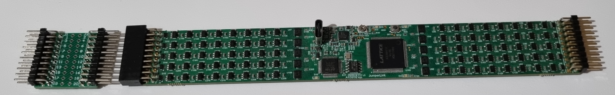
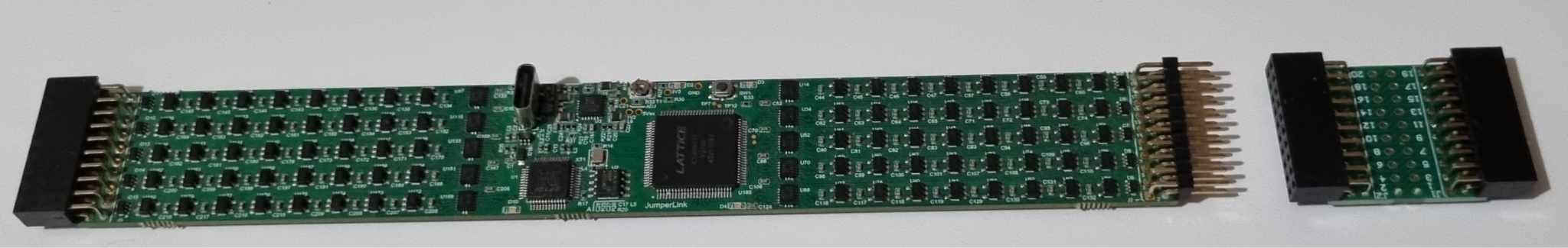
3. Hardware structure
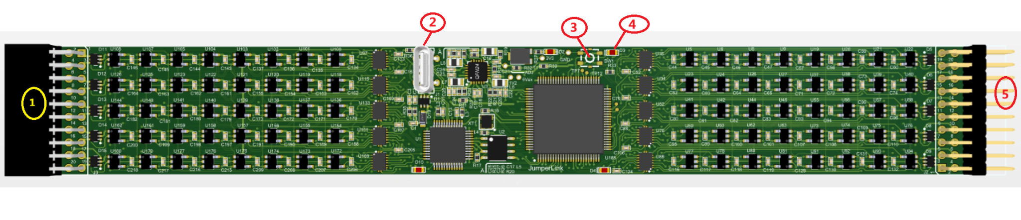
![]()
❶, Left-Side Connector The left-side connector provides 20 pins in a female header format for external device connections.
❷, USB Type-C Connector The USB Type-C connector is used to supply power to the board and to download configuration data.
❸, User Button Press the user button to toggle all links on both side connectors between enabled and disabled states.
When links are disabled, all pins on both connectors are set to a high-impedance state.
When links are enabled, pin functions operate according to the configured settings.
❹, User LED The user LED indicates the current link status. Different flashing rates represent whether the links are enabled or disabled.
❺, Right-Side Connector The right-side connector provides 20 pins in a male header format for external device connections.
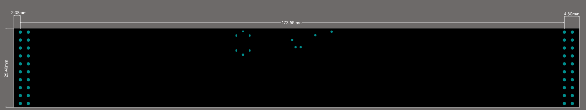
4. Dimension
![]()
5. Driver installation in Windows
The Jumperlink board uses an FTDI interface based on the FT232HL.
For most Windows operating systems, including Windows 10, the required FTDI driver is automatically installed by the OS. No manual driver installation is required for basic USB recognition.
However, to enable advanced communication with Jumperlink the driver must be replaced with libusbK.
Follow the steps below to replace the default FTDI driver with libusbK by Zadig:
1, Download Zadig from Internet
2, Right-click the Zadig executable and select Run as administrator.
![]()
3, Connect the Jumperlink board to your PC via the USB Type-C cable.
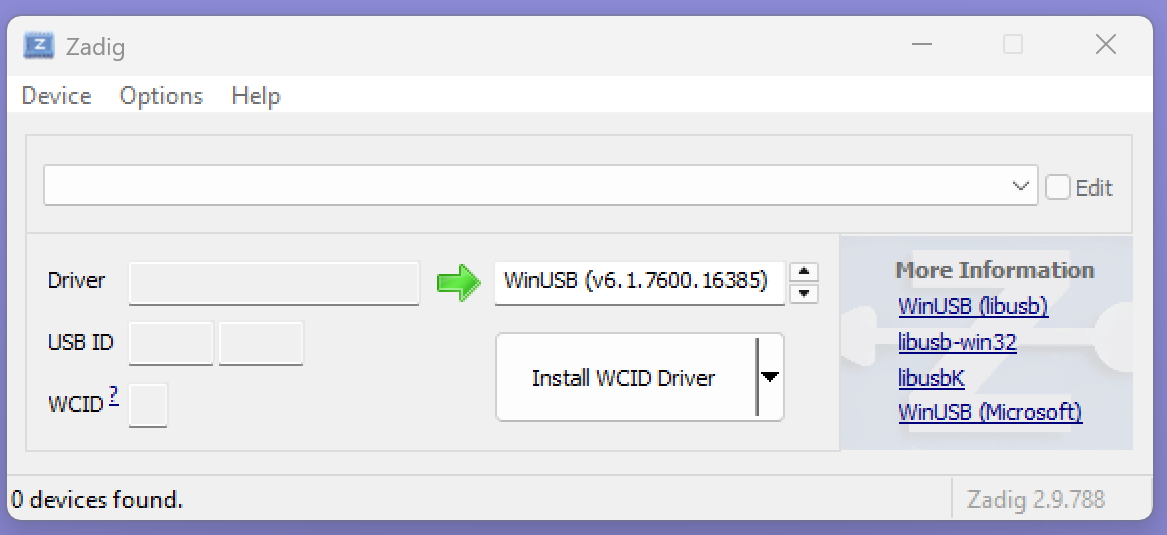
4, In Zadig, go to Options → List All Devices.
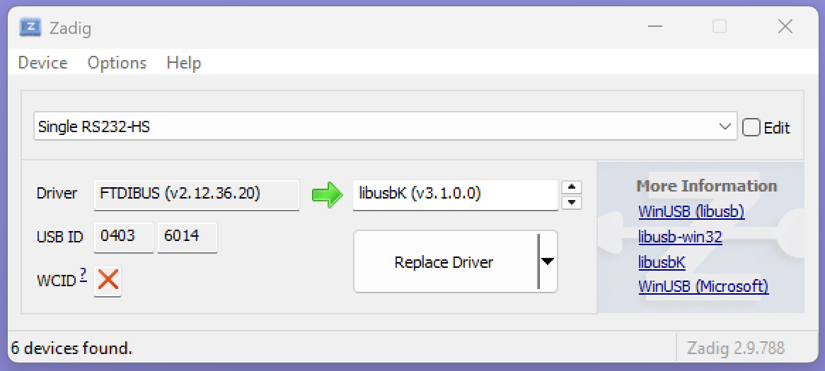
5, From the dropdown list, select the FTDI device (e.g., Single RS232-HS).
6, In the driver selection box, choose libusbK.
![]()
7, Click Replace Driver
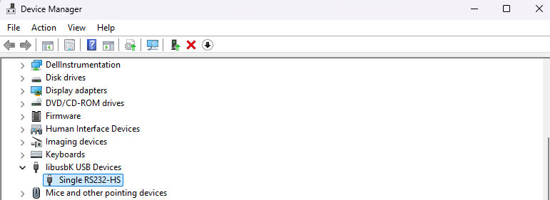
8, After completion, the device should now appear with the libusbK driver in Device Manager.
![]()
6. Driver installation in Linux
TBD
7. Jumperlink2
To enable flexible link configuration, Jumperlink provides a dedicated PC software tool called Jumperlink2.
Jumperlink refers to the hardware device, while Jumperlink2 is the configuration software used to control and program the board. The software allows users to define pin functions, create signal links, and generate configuration files that can be downloaded to the hardware.
Jumperlink2 provides the following features:
- Pin Type Selection Configure each pin as 5V, 3.3V, Ground, or Signal.
- Signal Linking Create connections between two pins when they are configured as signal pins.
- Configuration Download Download the generated configuration file directly to the Jumperlink board.
- Configuration File Management Save configurations as files on the PC. These files can be reopened, edited, and re-downloaded to the board when required.
- Pin Description Add simple text descriptions to each pin to make identification easier during configuration.
Follow the steps below to configure and program the Jumperlink board:
1, Open the Software
Launch the Jumperlink2 application on your PC.
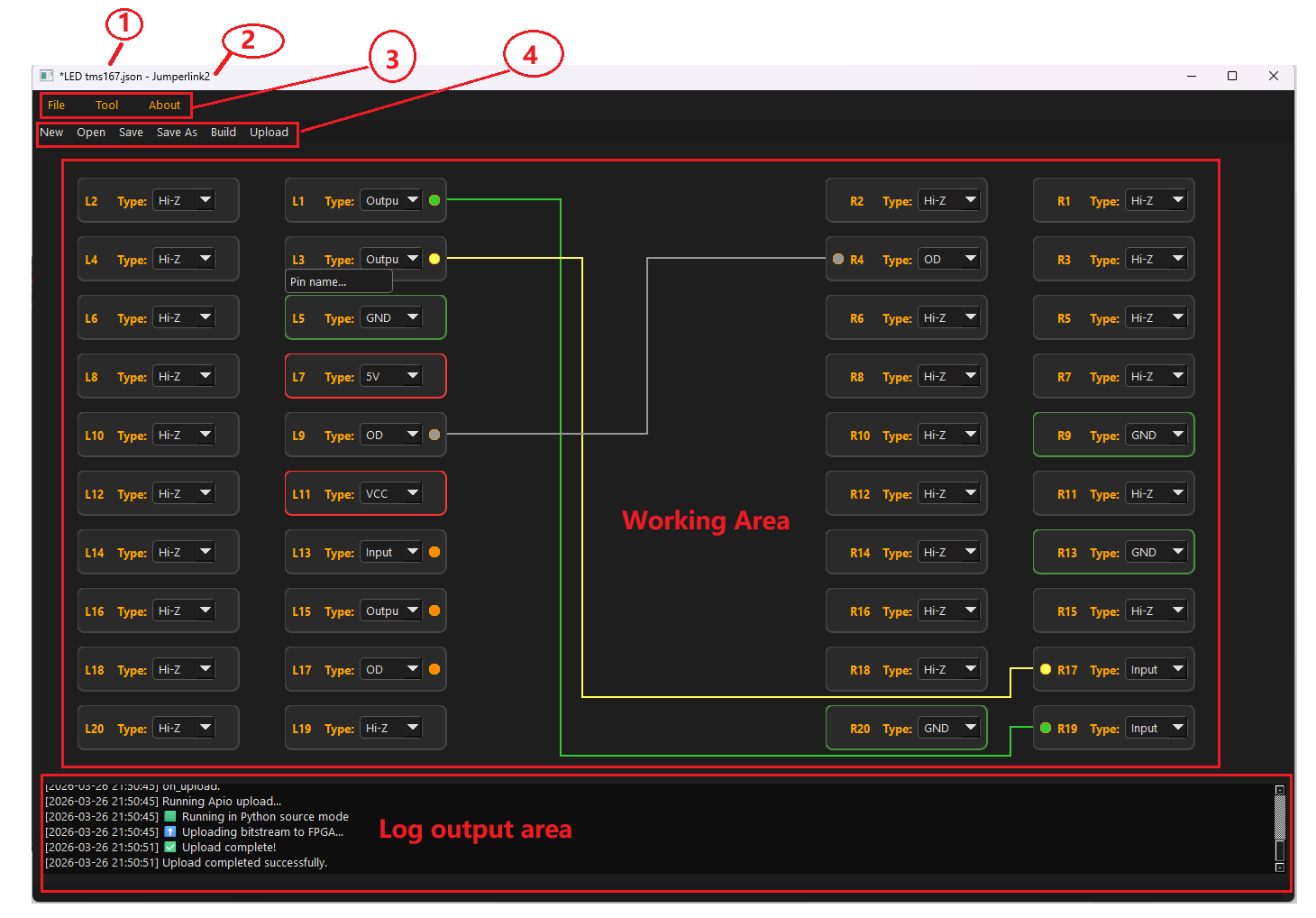
❶ , The currently opened file is shown in the top-left corner. For example, LED_tms167.json in the figure below.
❷ , The title Jumperlink2 appears at the top of the window.
❸ , A simple menu bar is provided for basic user operations.
❹ , A group of frequently used command buttons is located below the menu bar for quick access.
❺ , The central area of the application is the main working space where pin configuration and signal linking are performed.
❻ , The bottom section of the application displays log messages, including status information and operation results.
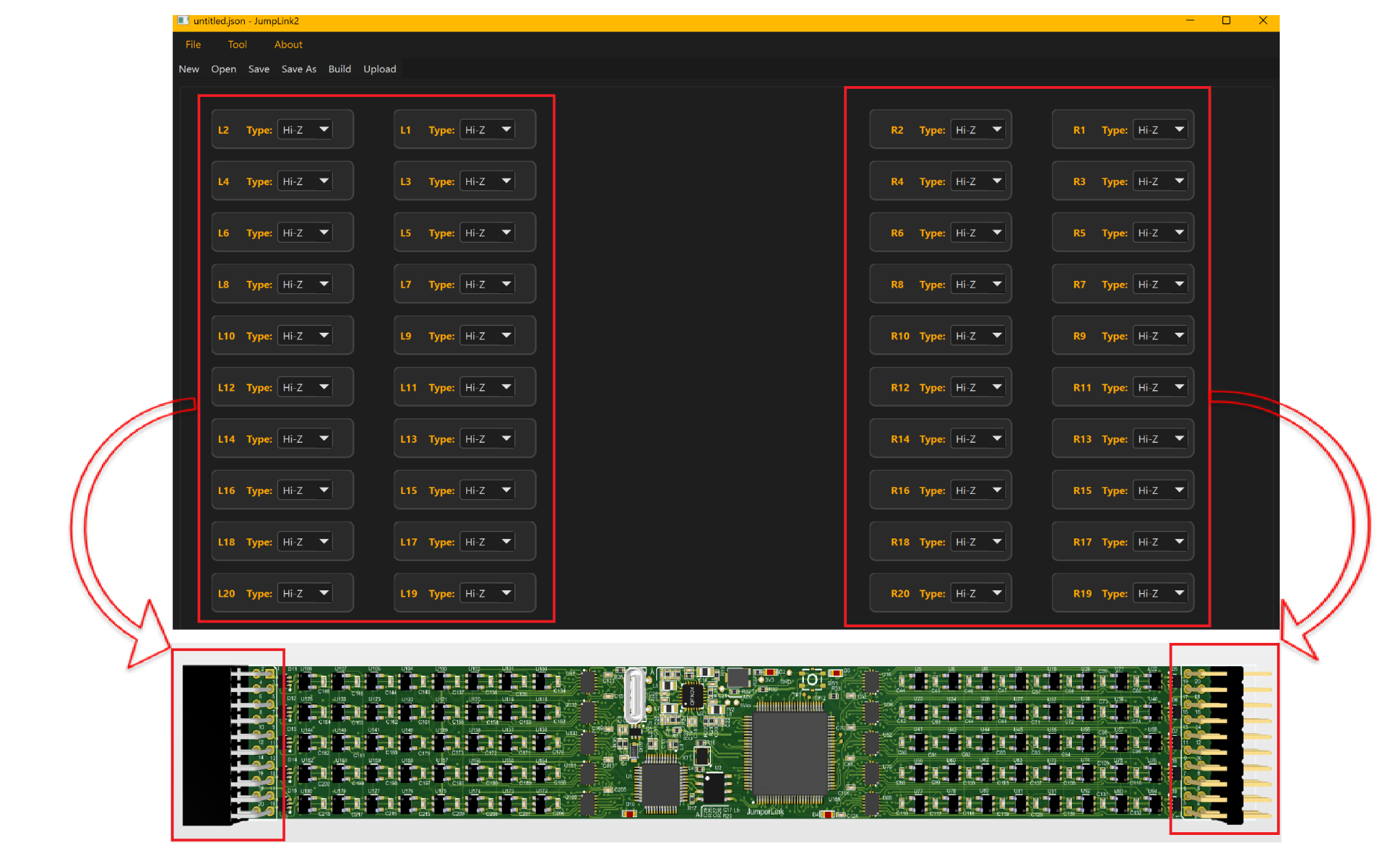
![]()
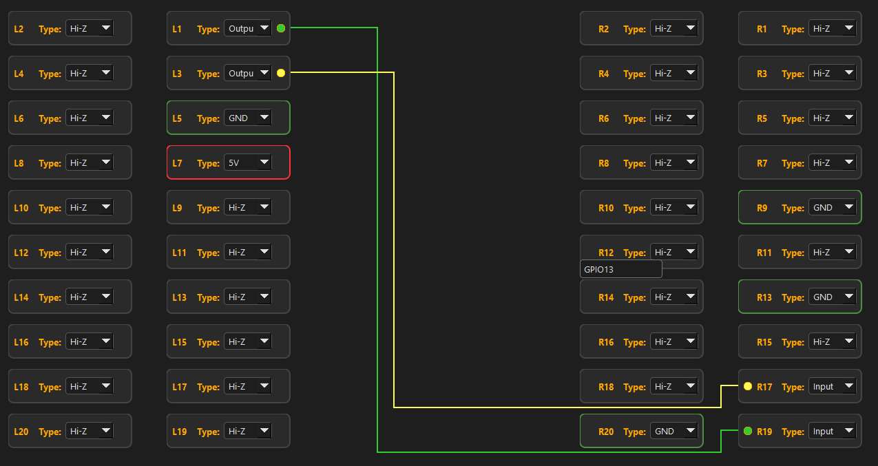
In the working area, there are 40 units in total, labeled L1–L20 and R1–R20.
They represent the 20 connector pins on the left side and the 20 connector pins on the right side.
![]()
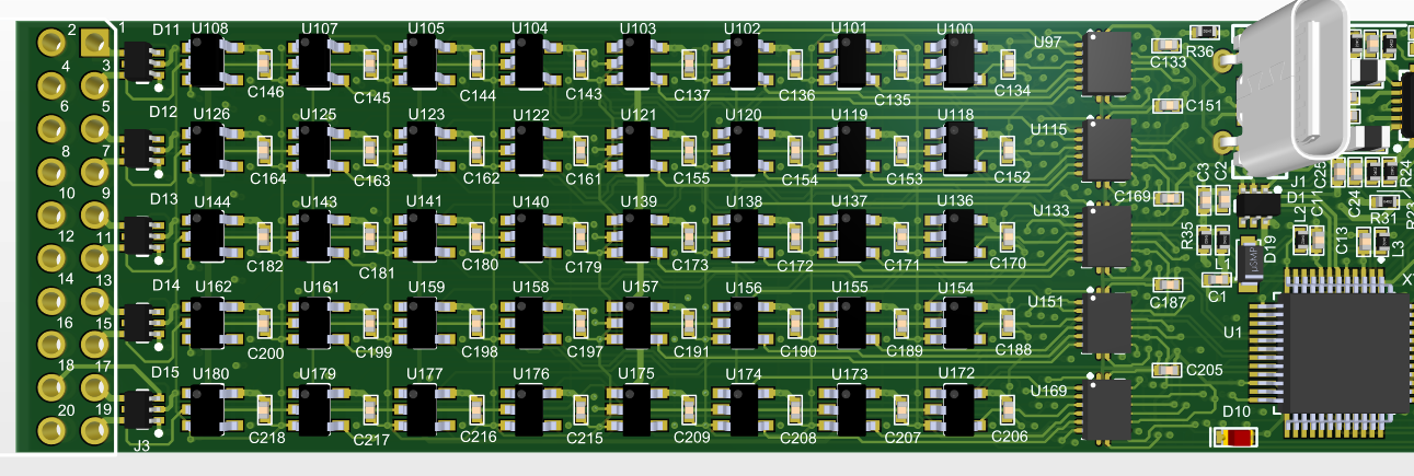
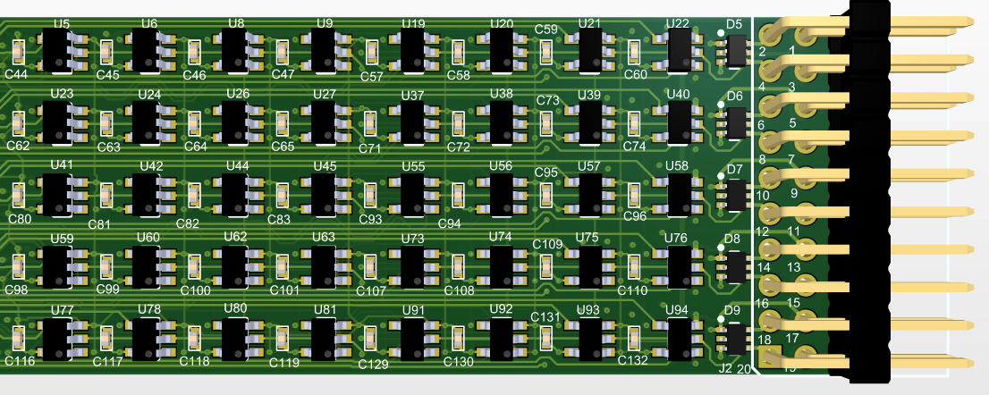
the Detail number of each pin:
![]()
![]()
2, Configure Pins and Links
Select the required pin type for each pin (e.g., 5V, 3.3V, Ground, or Signal) according to application.
![]()
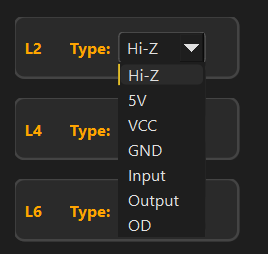
Each pin can be configured with 7 options:
Hi-Z
5V
VCC
GND
Input signal
Output signal
OD (Open-Drain) signal
the default set for VCC is 3.3V and the OD signal is mainly for I²C bus
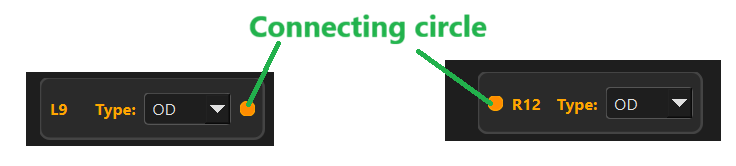
If a pin is configured as a signal (Input, Output, or OD), a connecting circle will appear next to the pin.
![]()
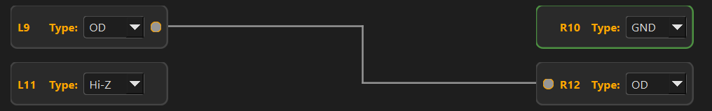
To create a link, click the connecting circles of two signal pins according to your application requirements. For example, clicking the connecting circles of L9 and R12 will automatically create a link between these two pins.
![]()
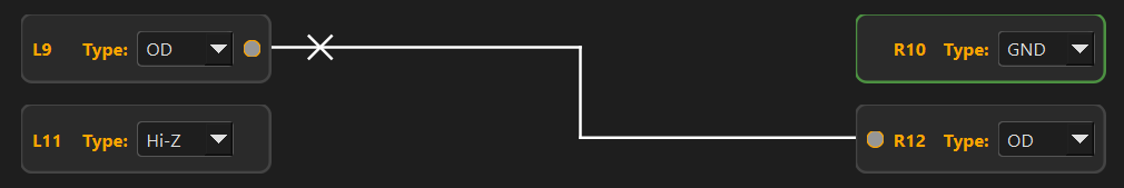
To delete a link, first select the link and then click the X mark displayed on it. Alternatively, changing either pin type from Signal to Hi-Z, 5V, VCC, or GND will automatically remove the link.
![]()
3, Save the Configuration
Click Save button or click File -> save to store the project file on your PC. The saved file can be reopened later for editing.
4 Build the Configuration File Click Build or Tool -> Build to generate the configuration .bin file.
if it is built successfully, the Log output will looks like this:
[2026-03-27 13:16:07] Build completed successfully.
5, Upload to the Board Connect the Jumperlink board to the PC using a USB type-c cable. Click Upload or Tool-> Upload to download the generated configuration file to the board.
[2026-03-27 13:22:42] Upload completed successfully.
6,Enable the Links on the Board
After the configuration .bin file has been downloaded, the User LED will flash slowly (3 seconds ON / 3 seconds OFF), indicating that the download was successful. At this stage, all pins remain in the Hi-Z (high-impedance) state.
Press the User Button to enable the configured links. When the links are enabled, the User LED will flash faster (1 second ON / 1 second OFF), indicating that the downloaded configuration is active.
Each time the User Button is pressed, the configuration will toggle between enabled and disabled states. The LED flashing rate indicates the current status.
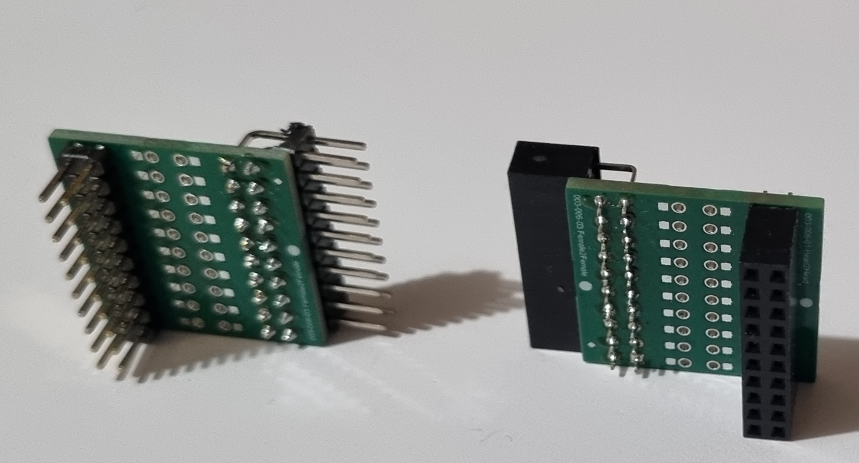
8. Extend boards
As the default connector types on Jumperlink are male on one side and female on the other, it is easy to connect two devices that use different connector types. However, this configuration may be limited when both external devices use the same type of connector.
For example:
A male-to-male (header-to-header) extension connector allows Jumperlink to connect to devices that have female headers on both sides.
![]()
A female-to-female extension board allows Jumperlink to connect to devices that use male pin headers.
![]()
Right-angle extension connectors are also available to support different mechanical layouts and make connections easier in space-limited setups.
![]()
These extension options allow Jumperlink to interface with a wide range of external devices and development boards.
9. Example:Connecting a Raspberry Pi I/O Board to a TM1637 LED Module
This example demonstrates how to use Jumperlink to connect a Raspberry Pi I/O board to a TM1637 LED display module without using traditional jumper wires.
1, Prepare the Hardware
The project requires the following components:
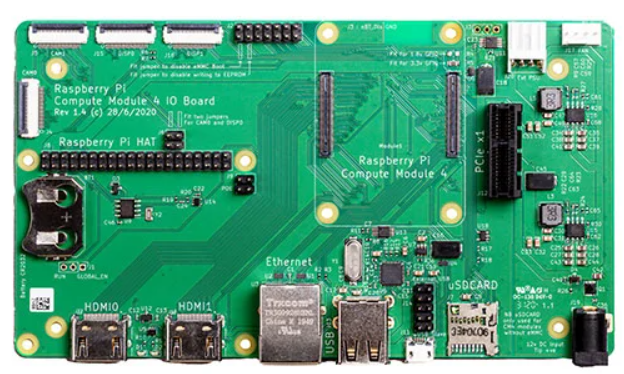
- Raspberry Pi I/O board
![]()
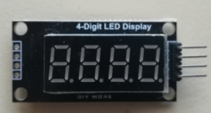
- TM1637 LED display module
![]()
- Jumperlink board
- extent board
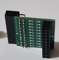
Since the TM1637 LED display module uses male pin headers and the J8 connector on the Raspberry Pi I/O board also uses male pin headers, a female-to-female extension board is required to complete the connection.
![]()
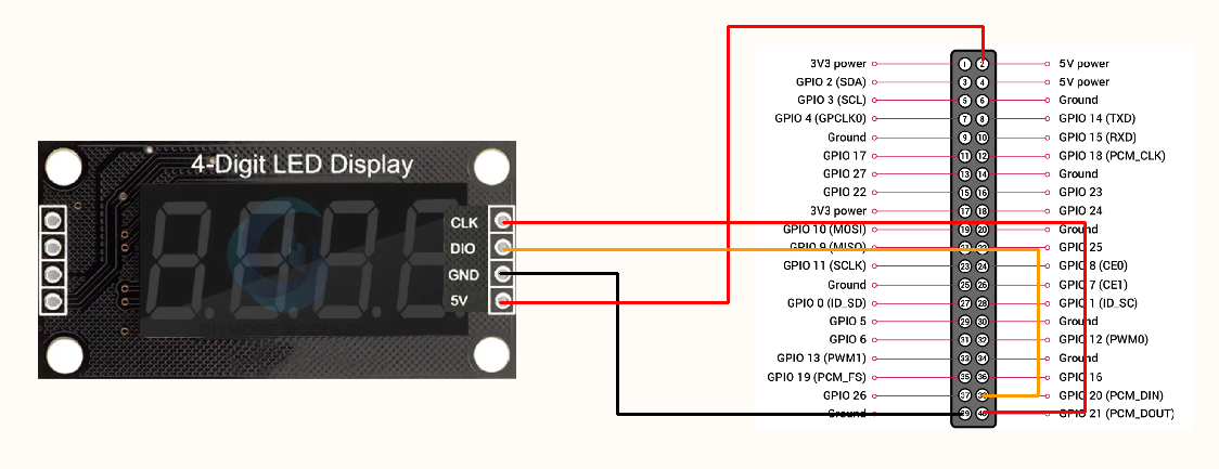
Normally, these two devices would be connected using four jumper wires. The required signals are:
- 5V
- GND
- CLK
- DIO
![]()
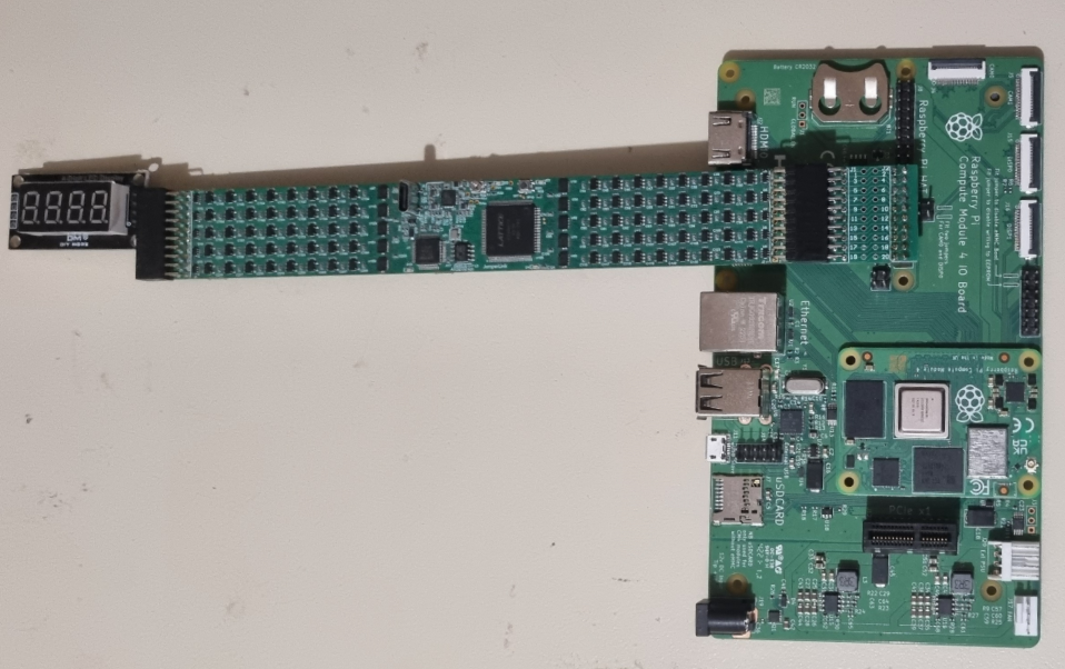
2. Connect Jumperlink to the Raspberry Pi I/O Board and TM1637 module
Attach the right-side connector of Jumperlink with the extent board,then to the lower section of connector J8 on the Raspberry Pi I/O board. When aligned with the bottom portion of the J8 header:
- R1–R20 on Jumperlink correspond to pins 21–40 of J8.
This alignment makes the pin mapping easier to follow and eliminates the need to repeatedly count header pins during setup.
while TM1637 module is connected to L1,L3,L5 and L7.
![]()
3,Configure the Pins in the Jumperlink Software
Open the Jumperlink2 application and configure the required signals.
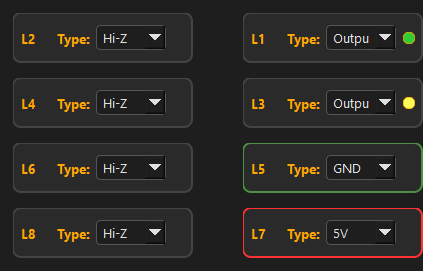
For this example:
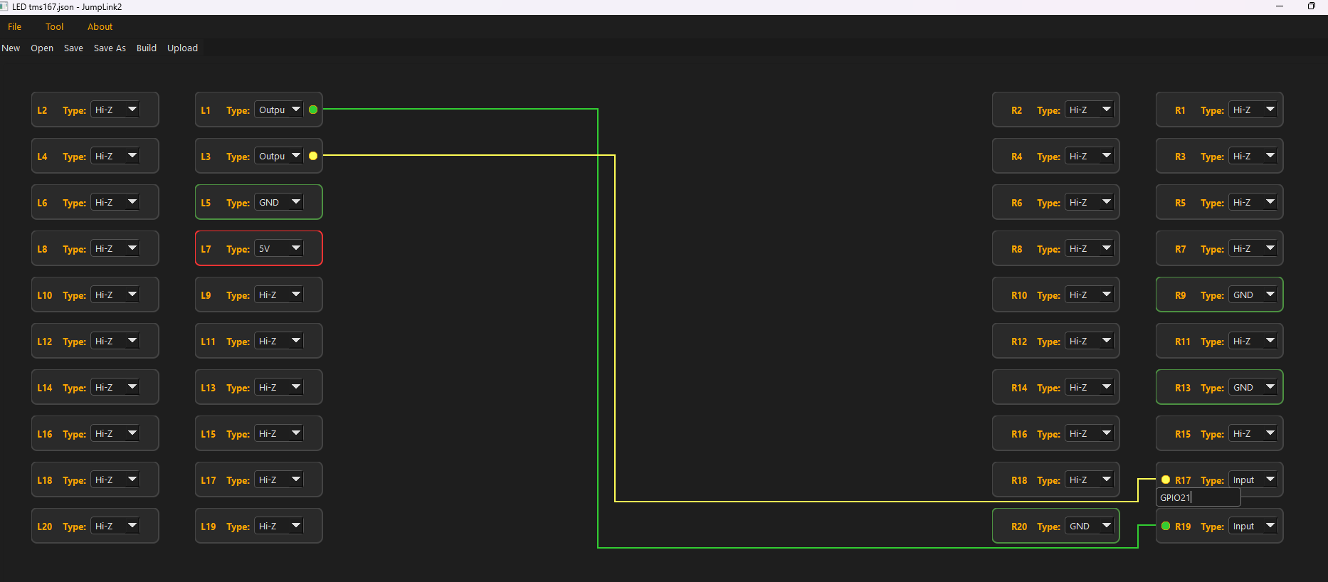
- Configure the pins L1,L3,L5 and L7 to match TM1637 module. L1 and L3 are all Output as the data direction will be from Jumperlink to TM1637.
![]()
- Configure the pins corresponding to GPIO20 and GPIO21.
![]()
- Create links in the software
![]()
L1 - R19 link is used for CLK of TM1637
L2 - R17 link is used for DIO of TM1637
There are no showing wires between IO board and TM1637 for power signals 5V and GND, because
Jumperlink would provide 5V to TM1637
L5 and R20 is connected by Jumperlink Ground plane.
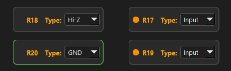
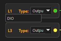
To improve clarity, name the pins in the software according to their actual functions. For example:
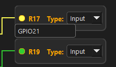
- name R19 as GPIO21, R17 as GPIO20, indicating the 2 pin are GPIO21 and GPIO20 from Raspberry CM4 module
![]()
![]()
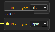
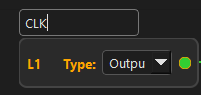
- Similarly name L1 as CLK, L2 as DIO to indicating the functions from TM1637 module.
![]()
![]()
Once complete, save the project file.
![]()
4,Build and Download the configuration to Jumperlink
Click Build or Tool -> Build to generate the configuration .bin file.
if it is built successfully, the Log output will looks like this:
[2026-03-29 18:00:59] on_build.
[2026-03-29 18:00:59] Updating verilog files...
[2026-03-29 18:00:59] Running Apio build...
[2026-03-29 18:00:59] 🟩 Running in Python source mode
[2026-03-29 18:01:01] 🔧 Starting FPGA build flow...
[2026-03-29 18:01:07] ✅ Build complete! Output: build.bin
[2026-03-29 18:01:07] Build completed successfully.
Click Upload or Tool-> Upload to download the generated configuration file to the board.
if it is upload successfully, the Log output will looks like this:
[2026-03-29 18:32:36] on_upload.
[2026-03-29 18:32:36] Running Apio upload...
[2026-03-29 18:32:36] 🟩 Running in Python source mode
[2026-03-29 18:32:36] ⬆️ Uploading bitstream to FPGA...
[2026-03-29 18:32:42] ✅ Upload complete!
[2026-03-29 18:32:42] Upload completed successfully.
Please note:
The real output log will be subject to change after software updating to new reversion.
After the configuration .bin file has been downloaded, the User LED will flash slowly (3 seconds ON / 3 seconds OFF), indicating that the download was successful. At this stage, all pins remain in the Hi-Z (high-impedance) state.
Press the User Button to enable the configured links. When the links are enabled, the User LED will flash faster (1 second ON / 1 second OFF), indicating that the downloaded configuration is active.
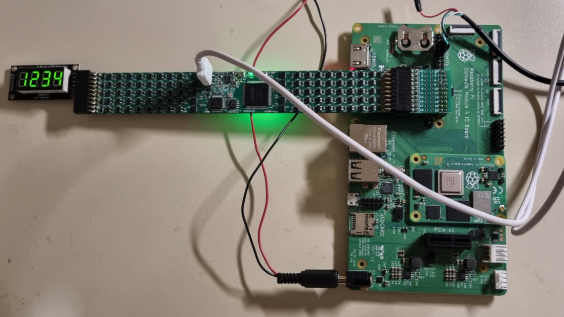
5, Test the function of TM1637
Run the driver software of TM1637 on Raspberry Pi software, and the program runs as expected
![]()
10. More Examples
TBD
Jumperlink: A Smarter Way to Connect Electronics
Jumperlink is a board designed to make electronic connections easier to set up, maintain, and share compared to traditional jumper wires.
Discussions
Become a Hackaday.io Member
Create an account to leave a comment. Already have an account? Log In.