 dylan zheng
Most electronic engineers or hobbyists have used jumper wires, particularly when starting their first projects with a breadboard. This is quite good for quick prototyping.Students and hobbyists can easily modify circuits to see how changes affect behavior, which is invaluable for understanding electronics principles hands-on.

but then you definitely will find out the notable disadvantages, such as unreliable connections during debugging and testing. It is exhilarating when starting a project. However, frustration inevitably creeps in when you discover that your system isn't working because a wire is loose, or you need to reassemble it after a few weeks, struggling to remember how to reconstruct your project. The most discouraging part is realizing that a project built with jumper wires is delicate and messy. I give up, those are the final words when that day eventually comes.
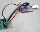
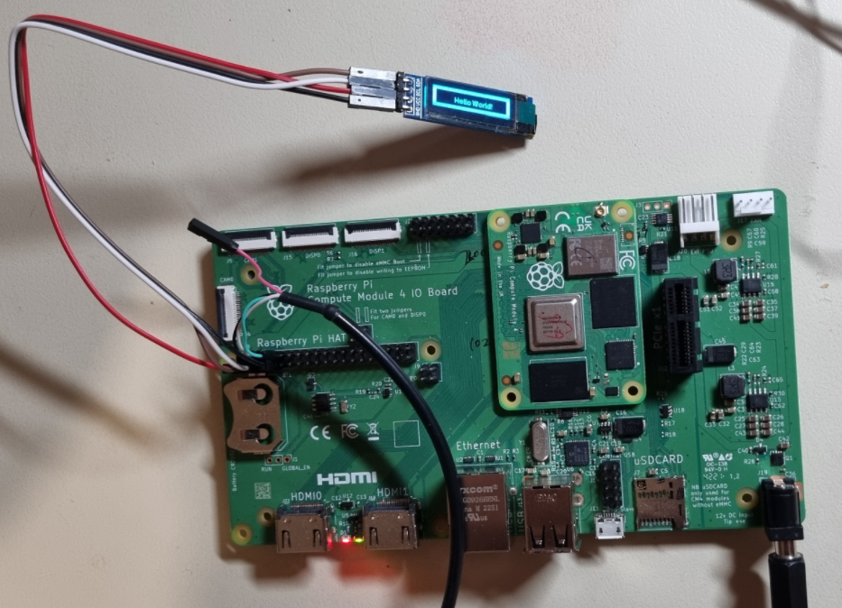
I have to spend hours to rebuild below project when I need to do a simple test:

Let's carefully recall our minds and list all the issues for the jumper wires:
1, Jumper wires are easy to lose connection after certain times of plugging in and out.
2, Jumper wires are NOT suitable for high speed
3, Jumper wires are NOT friendly for debugging, NOT friendly for signal testing with oscilloscope probes.
4, Jumper wires are good for very simple projects, but they become messy when more cables are added in.
5, Jumper wires are hard to set up when more than 10 wires have to be used
6, Jumper wires are fragile and have to be handled very carefully when moving a project setup from one place to another.
7, Jumper wires are tough to maintain the settings, especially need to be re-set up several weeks later.
8, Jumper wires are consumables, and you will find there are no cables available in your drawers after a certain time no matter how many you have bought, you have to borrow some wires from another project, which is carefully stored in your cabinet. This again makes you headache when you have to re-set up “another project” in the future.
9 Other issues, for example, the head pin of jumper wires accidentally touches a PCB and gets the PCB board spike.
So, is there any other option to overcome the shortages listed above? What alternatives are available for replacing jumper wires?
The answer was NO when I searched it over the internet.
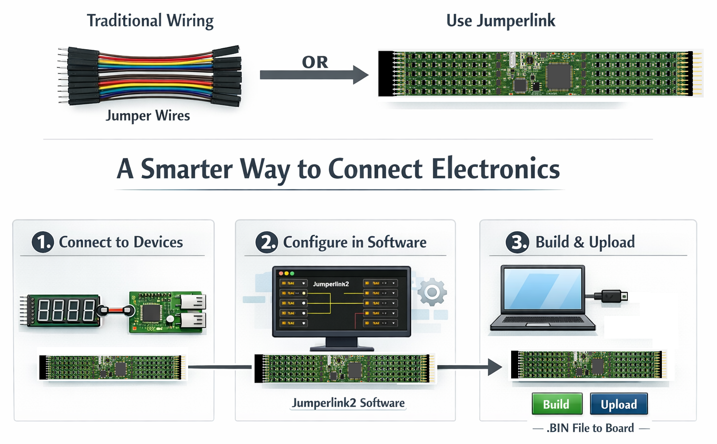
As an electronic engineer, I thought this was quite a good point for me if I could design a board to fix most problems listed above and that's where my solution comes in—I've developed a new board called the "JumperLink."
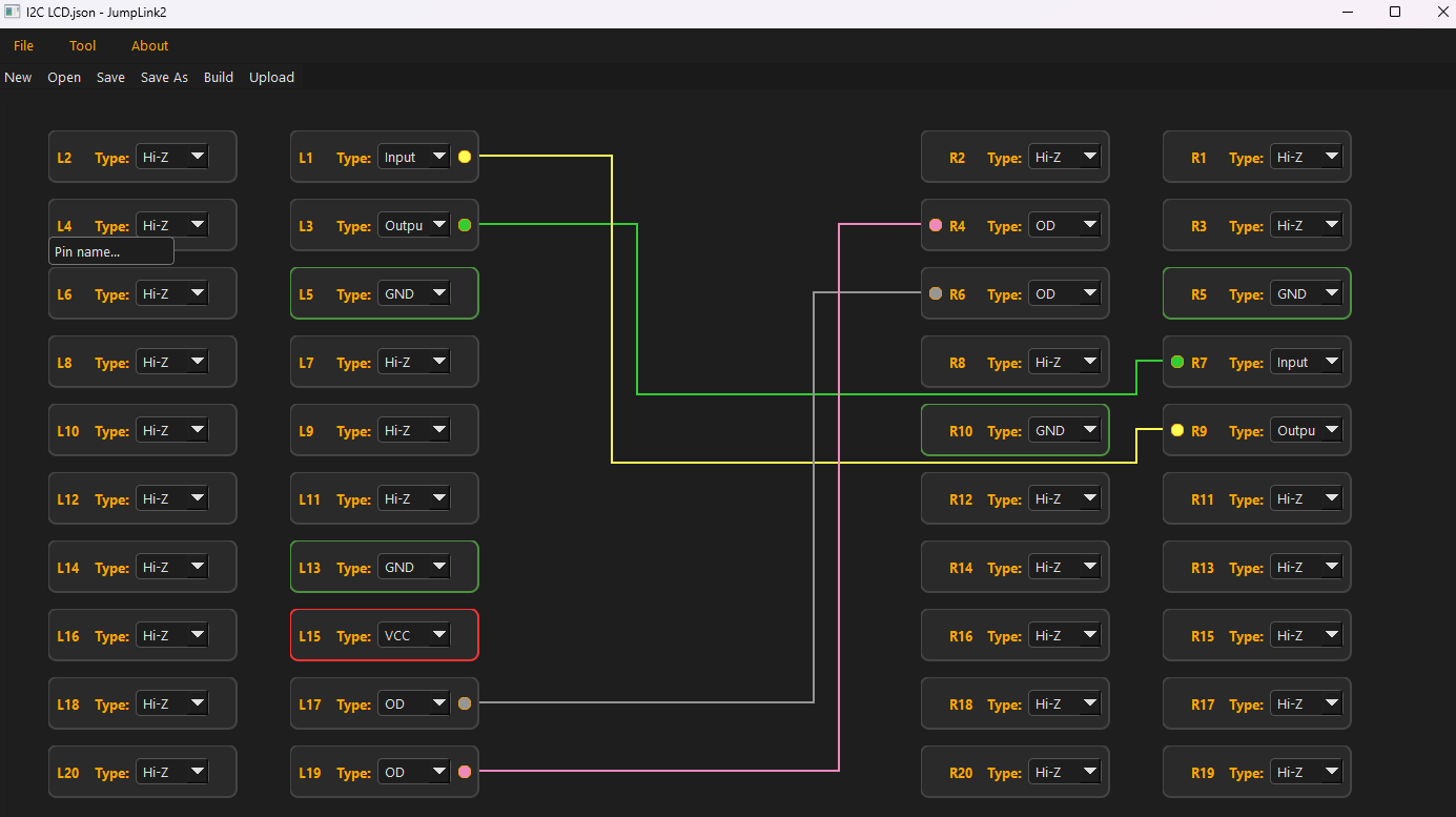
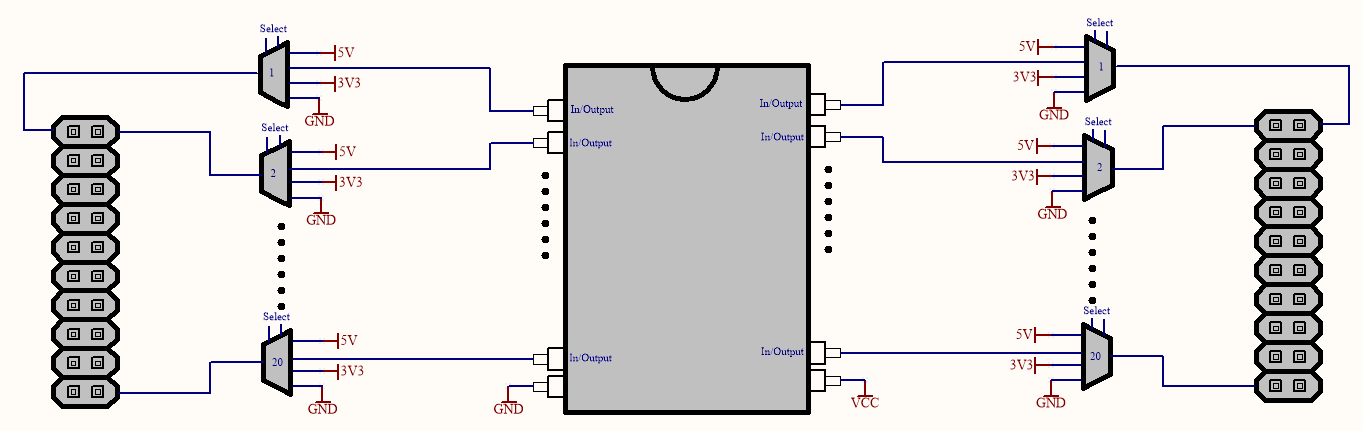
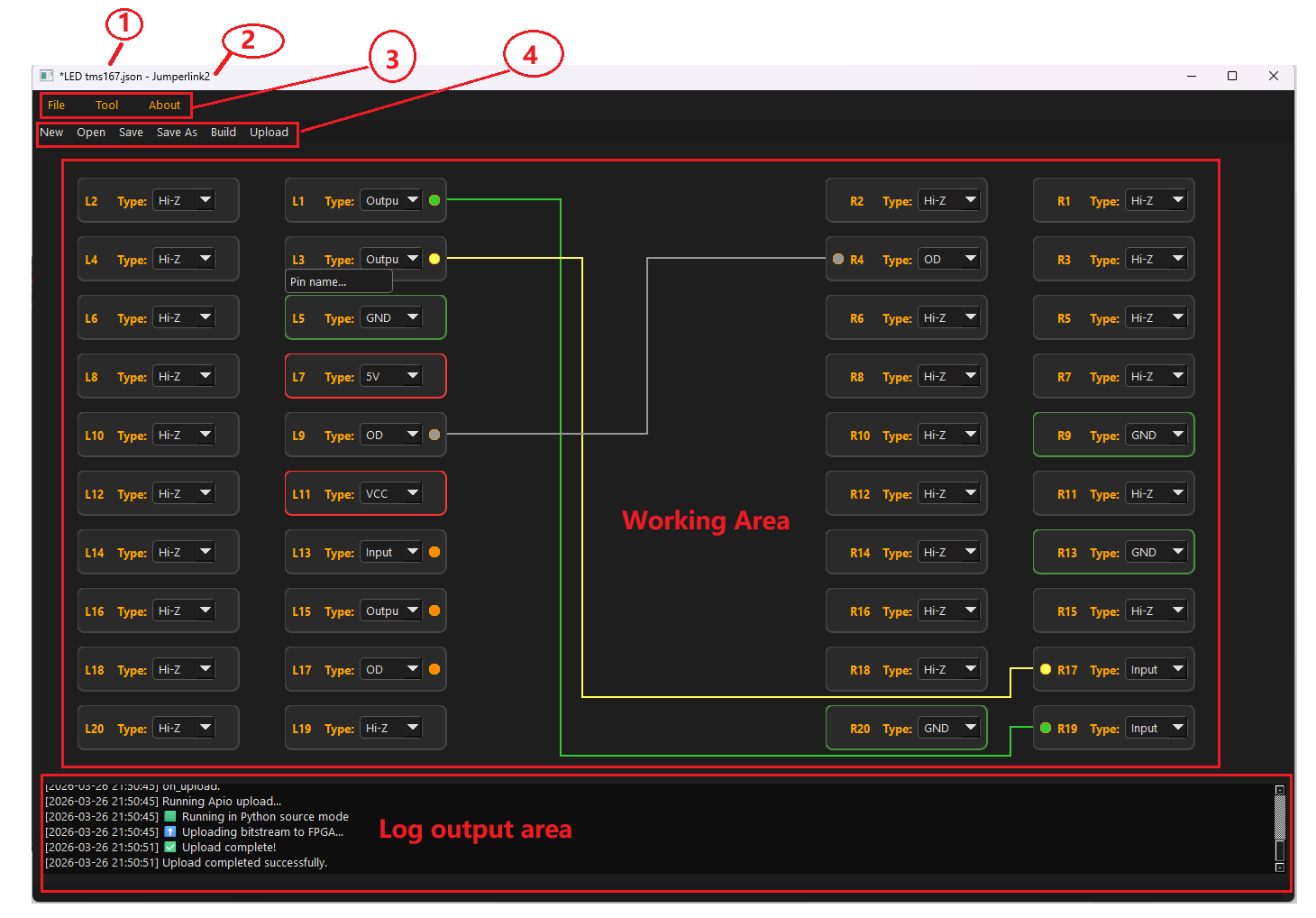
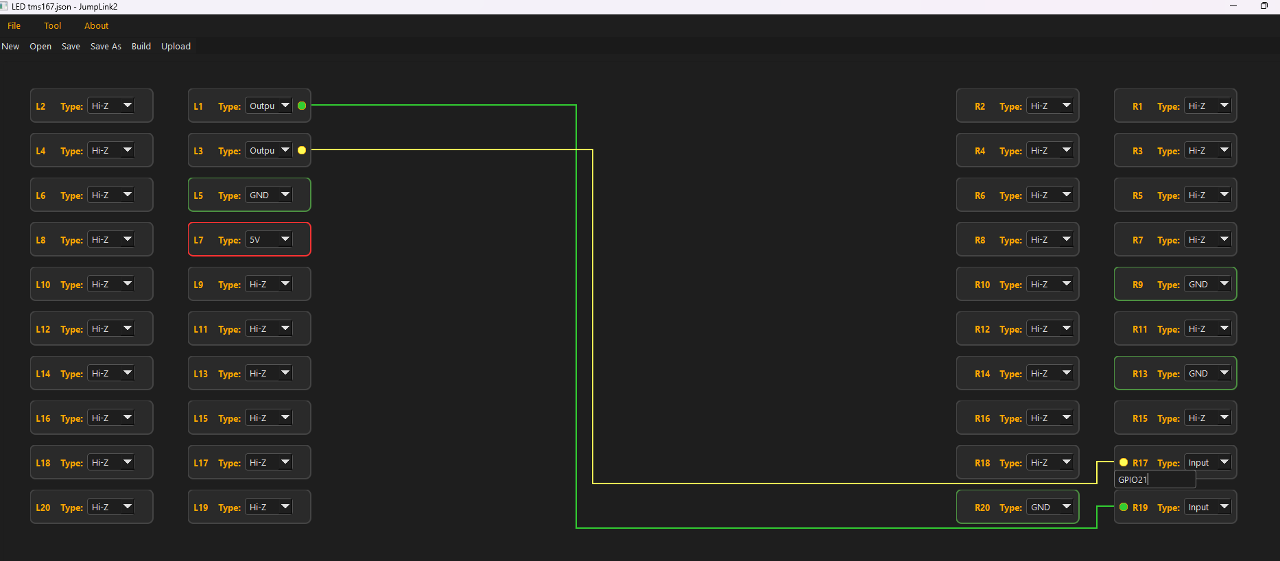
What is a Jumperlink?
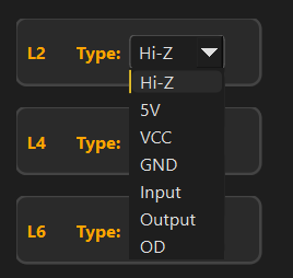
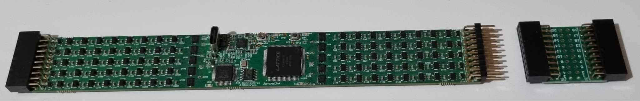
A Jumperlink is a board with a FPGA on and provides a configurable switch function for external connections.
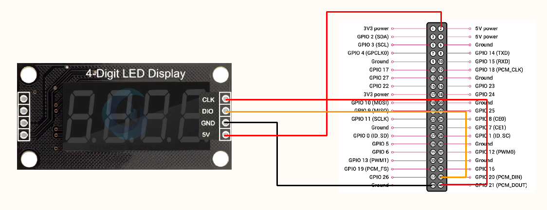
A diagram will be much more useful than any words.
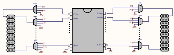
The basic idea comes from my experience using jumper wires. Any one wire will be connected to power or a signal. so I asked myself if I could make a connector with any pin that can be configured as a power output or signal input/output by software, then it is able to be used to connect most external devices. those external devices which are easy to purchase from online, such as from sparkfun or aliexpress etc.
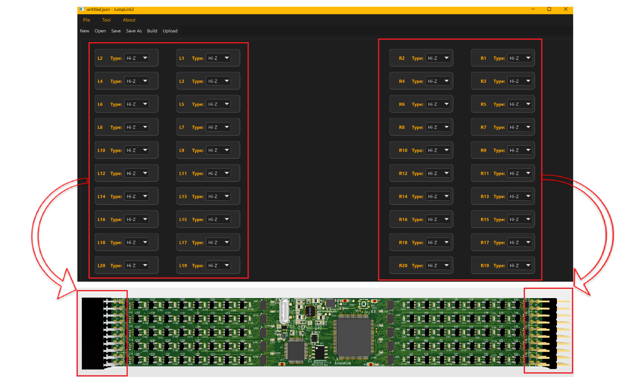
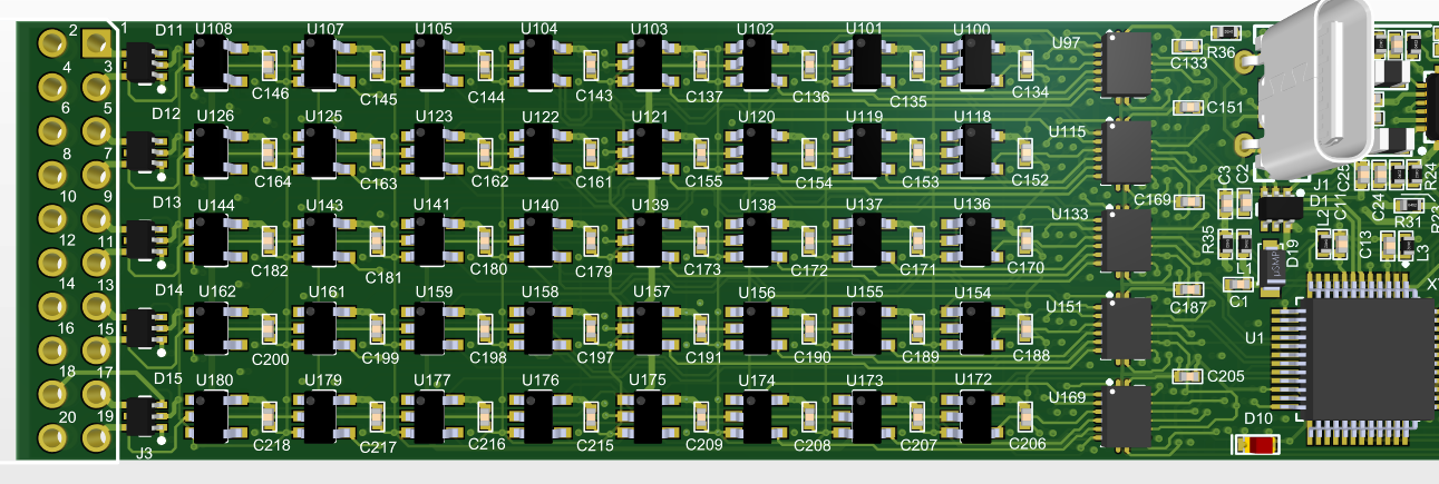
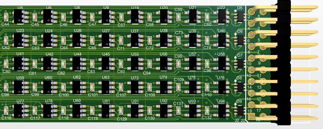
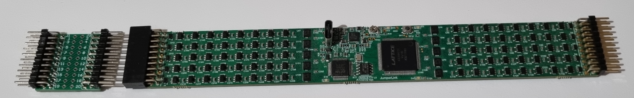
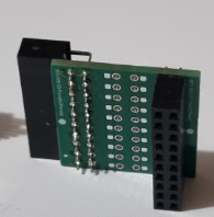
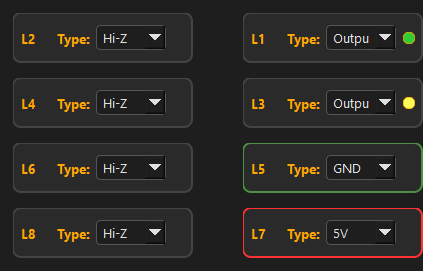
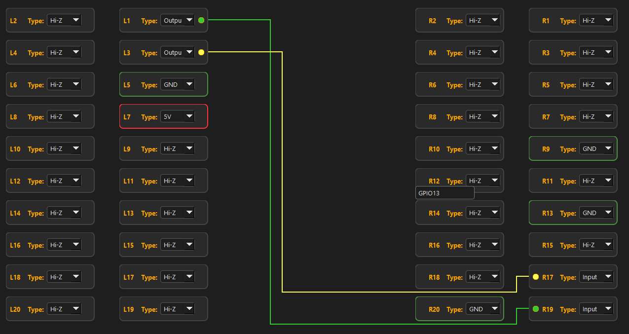
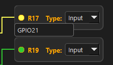
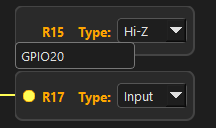
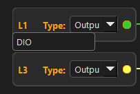
As shown in the picture, Jumperlink has one FPGA in the middle and 20 pins on both left and right sides which is symmetrical in design. a multiplexer is added to each pin between FPGA and connectors, which makes each pin of the board able to be connected to 5V, 3.3V, signal and Ground. All signals are connected to a FPGA in which all of them are able to be configured from software. 3.3V and 5V are selected because they are the most common power in the embedded world.
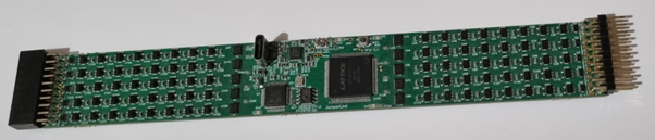
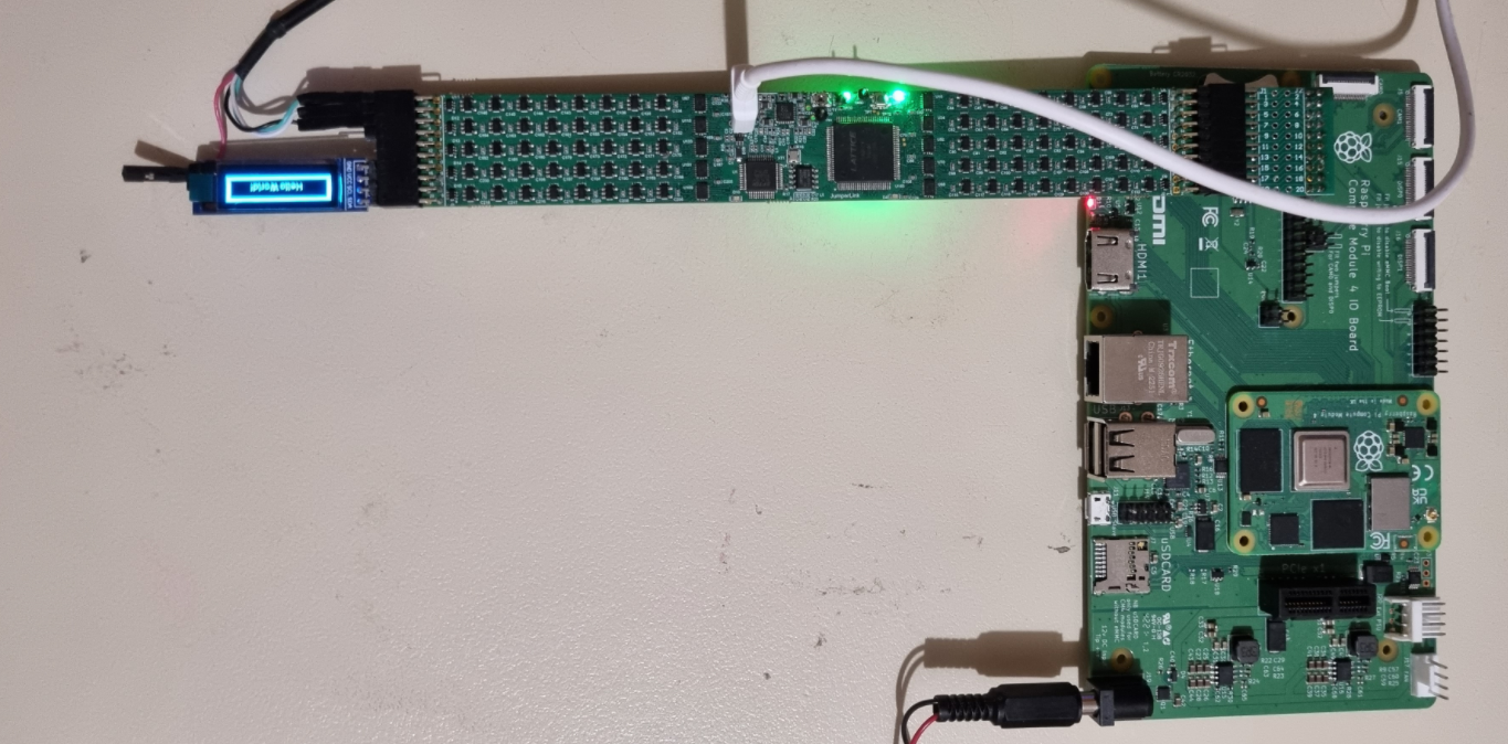
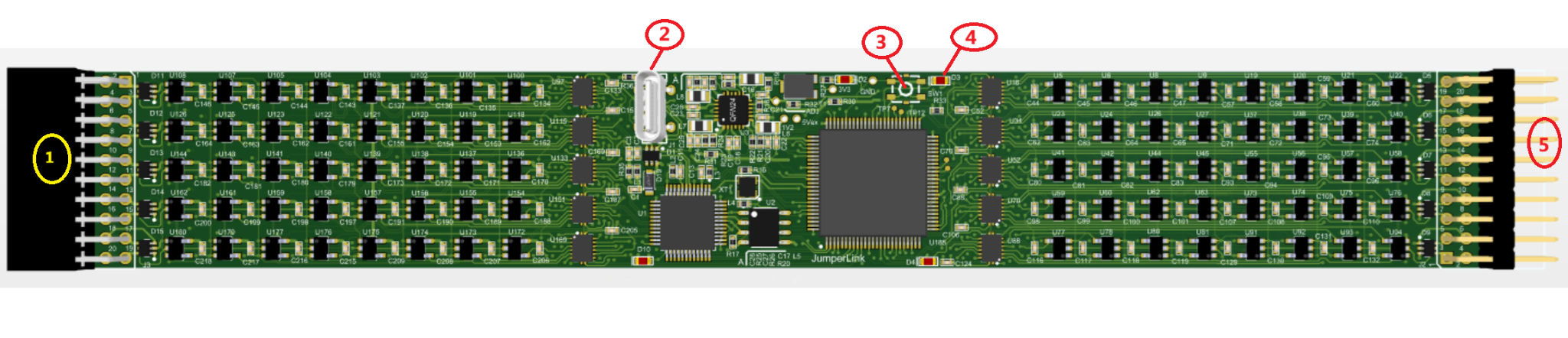
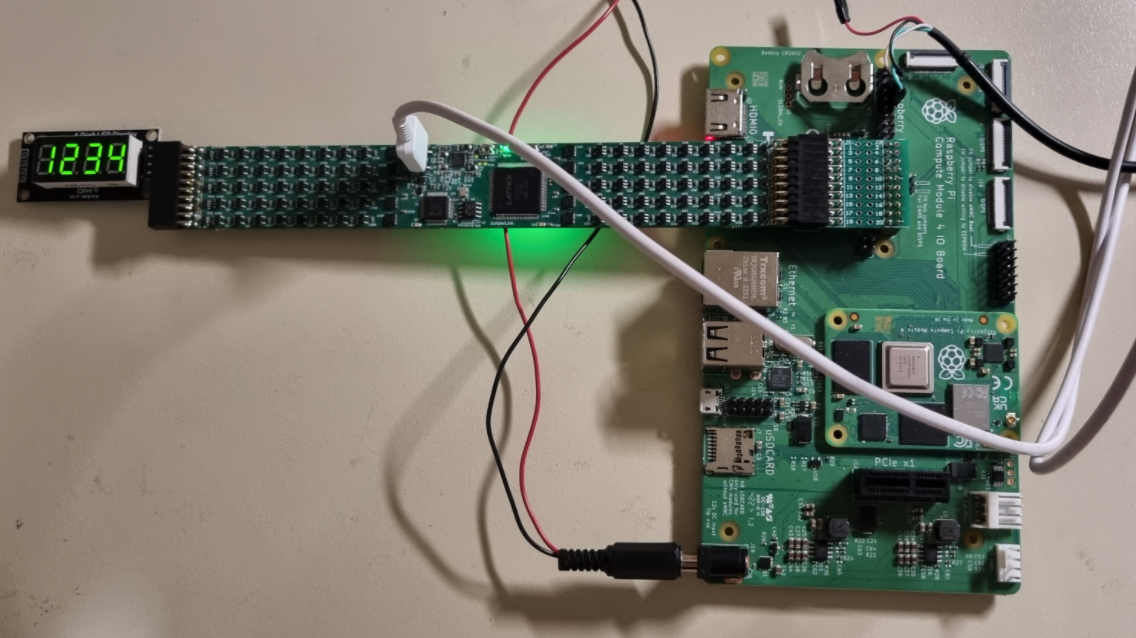
this is the PCB I completed:
More details about Jumperlink
Jumperlink includes many useful features. Below is a summary of the key highlights:
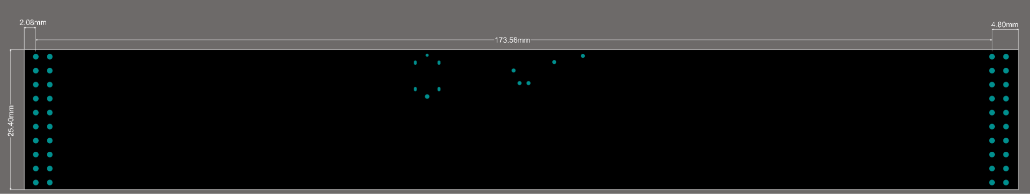
1, Board size: 180 mm × 25.4 mm
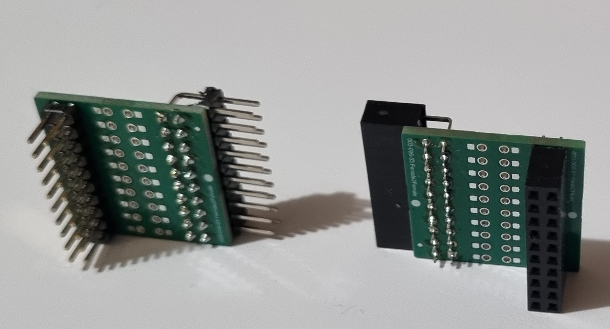
2, Uses standard 2.54 mm pitch headers/connectors
3. Provides...
Read more »


 mit41301
 Hans Jørgen Grimstad
 James Stallings
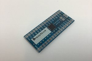
 Ben Lim