 Zduka
So with the recent Puya tests, I started being very optimistic about the chip and decided to enter the therapeutic phase of PCB layout & routing. This is mkIV as there is no hope of backwards compatibility after the IO MCU change (I mean the SDK is generic enough so that this might be achievable, but absolutely not worth it) and so far I am really pleased with it. For the first time the routing feels intentional, not hacked.
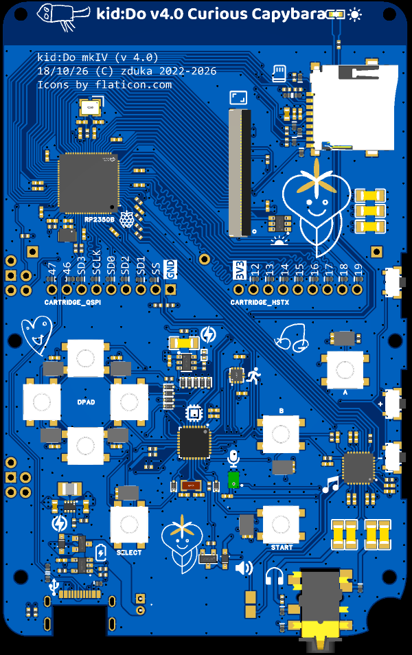
Along the way, I have realized a few things that led to even further BOM optimizations:
- the new RGB LEDs not only run from 3v3, but they also have standby current of just 1uA (as opposed to the neopixel standard 1mA) which means I can ditch the 5V charge pump as well as the rail switch
- the rail is thus not necessary simplifying the power routing
- device power on is done via dedicated switch with overcurrent protection and soft start so that high capacitance, or even shorted cartridges should not damage the system
- accelerometer is connected via SPI to the PY32F030 to completely isolate the always on power domain
- ESD protection on the cartridge pins
- SD card ESD & pullups in discrete parts since the CM1624 proved rather complex to source (and more expensive)
- simplified routing around the PUYA and Audio codec (different orientation)
- standardized debug port for RP2350 and PY32F030
- smaller & better suited signal diodes for the button matrix
- better side buttons
- light sensor above the display with a single LED (instead of I2C costly detector)
I am 99.9% finished with the layout - the only thing that remains is the correct capacitor values around the 32kHz crystal which I have to figure out.
And I am not ordering anything yet, letting the new design sink a bit, probably adding some finishing touches a bit later. I would really, really want this to be the last pre-production version, so please, feel free to comment:-)
Discussions
Become a Hackaday.io Member
Create an account to leave a comment. Already have an account? Log In.