 Masahiro Furukawa
Progress Report: ADX Core V0 Design Freeze and PCBA Order Placed
The design phase for the ADX Core V0 is officially complete. I have finalized the schematics and PCB layout, and the project has moved into the manufacturing stage. The PCBA (Printed Circuit Board Assembly) order has been placed with JLCPCB.
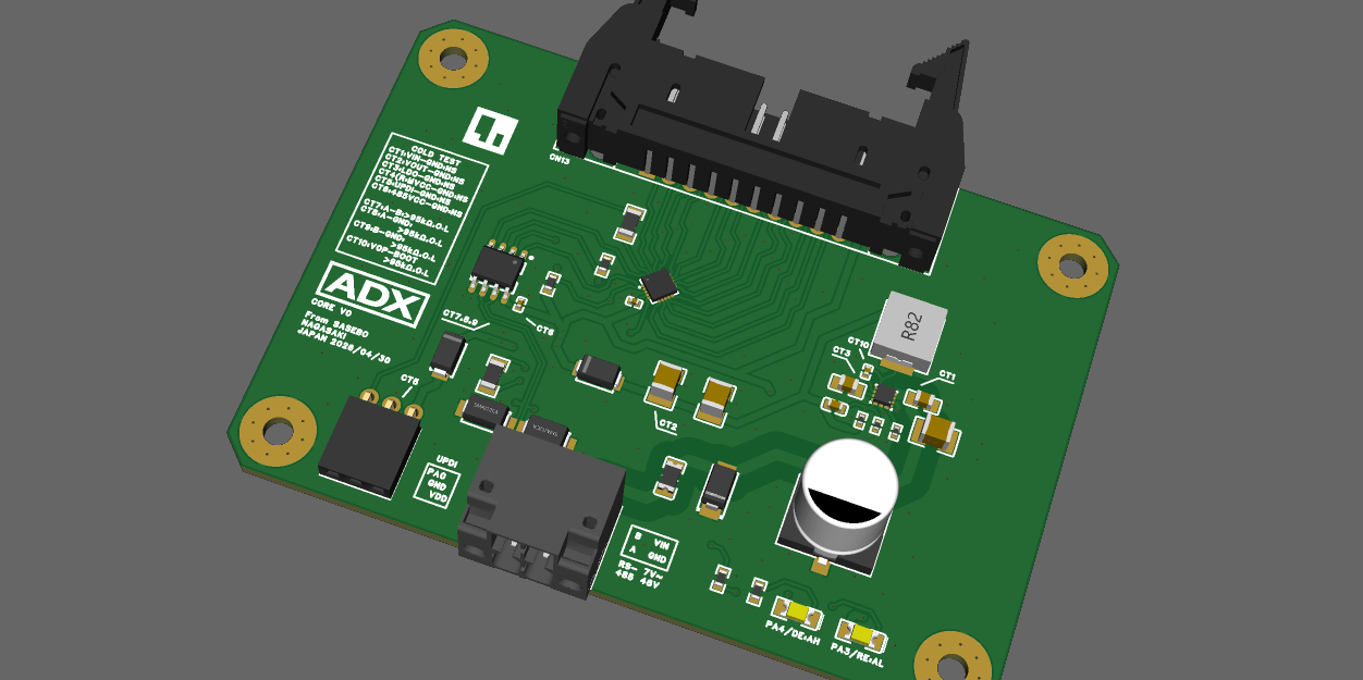
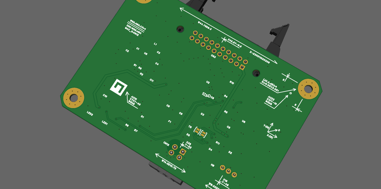
Status Update
- Schematics: Completed
- PCB Layout: Completed
- Manufacturing: In progress (Ordered via JLCPCB PCBA service)
- Target Grade: Industrial / Robust Control
Project Resources & Documentation
All design files, fabrication data (Gerbers, BOM, CPL), and detailed development history are available on GitHub:
Repository:
Note: The repository contains documentation and commit messages in a mix of English and Japanese.
Hardware Specifications
The ADX Core V0 is designed as an "Arduino-like" industrial control board. It introduces a new, standardized industrial form factor—inspired by the ATX philosophy—aimed at creating an ecosystem where enclosures and components are easily interchangeable and professional.
1. Performance Specifications
| Item | Specification | Notes |
| MCU | Microchip ATtiny1616-MNR | 8-bit AVR® megaAVR 0-series |
| Clock Speed | 20 MHz (16 MHz recommended) | Internal clock |
| Logic Voltage | 5 V | |
| Memory | Flash 16 KB / SRAM 2 KB / EEPROM 256 B | |
| Operating Temp | -40°C to +105°C | Industrial grade components |
2. Power & Protection
| Item | Specification | Notes |
| Nominal Input | DC 12 V / 24 V / 48 V systems | |
| Input Range | DC 7.0 V to 48.0 V | |
| Protection | SMD Chip Fuse / Reverse Polarity | |
| Surge Protection | TVS Diodes | Mounted on power input |
| Connection | 2-pin Push-in Terminal | Pluggable with lock lever |
3. Communication & Interface
| Item | Specification | Notes |
| Protocol | RS-485 x 1 channel | |
| Protection | TVS Diodes | A / B line protection |
| Programming | UPDI | 3-pin socket (UPDI, VDD, GND) |
4. GPIO Pin Assignment
Connector: 2×10 pin Locked IDC Box Header (Right Angle)
The layout utilizes multiple GND and VDD pins to ensure signal integrity and stable wiring in industrial environments.
| Pin | Signal | Notes | Pin | Signal | Notes |
| 1 | VDD | 5V Out | 2 | GND | Ground |
| 3 | PC3 | GPIO | 4 | PC2 | GPIO |
| 5 | PC1 | GPIO | 6 | PC0 | GPIO |
| 7 | GND | Ground | 8 | PB0 | GPIO |
| 9 | PB1 | GPIO | 10 | PB2 | GPIO |
| 11 | PB3 | GPIO | 12 | GND | Ground |
| 13 | PB4 | GPIO | 14 | PB5 | GPIO |
| 15 | GND | Ground | 16 | PA7 | GPIO |
| 17 | PA6 | GPIO | 18 | PA5 | GPIO |
| 19 | GND | Ground | 20 | VDD | 5V Out |
5. Mechanical Specifications
- Dimensions: 85.0 mm × 60.0 mm
- Mounting: 4 x M3 screw holes (corners)
- Features: 8.0 mm washer clearance, C3 chamfered edges.
Next Steps
Once the boards arrive from the fab, I will proceed with:
- Power rail verification: Testing stability with 24V and 48V inputs.
- Firmware upload: Initializing the ATtiny1616 via UPDI.
- Stress testing: RS-485 communication reliability in high-noise environments.
Discussions
Become a Hackaday.io Member
Create an account to leave a comment. Already have an account? Log In.