Parallel Logic
-
Infrared Communication - Sending a 1-second tweet
35 minutes ago • 0 commentsI've mentioned previously that part of my motivation for this project was the rock paper scissors concept presented at Supercon 2025 and before that at Burning Man, but wanted to expand on that to encourage longer interactions. I was also inspired by the RF badge at Supercon 2025 that served as an interesting platform to host a bot in. So I wanted to make a SAO that could exchange messages, and short messages between users naturally gravitates towards the concept of sharing "tweets".
Having interacted with the device in the video above, it was a little troublesome to make electrical contact, plus it complicated mass production, so I sought to make a contact-less solution. However, I've shied away from true RF like WiFi and BLE in part due to the extra resource requirements (either requiring an auxiliary chip or delving in with an ExpressIf solution), and in part because of the hacking-concentric nature of DEFCON and my own unfamiliarity with securing/hardening that kind of solution. So that left with Infrared as being a more traditional solution better suited to line-of-sight and short distances.
Each vendor of a TV or other device responding to IR has a slightly different implementation, but categorically you're talking about a ~940 nm wavelength LED emitting light. To avoid interference from static sources like light bulbs or otherwise, the protocol actually defines the active state as transmitting pulses of IR light at ~38 kHz, and the inactive state as transmitting no light at all. The traditional protocols also tend to define the data in terms of the length of the signals transmitted - so 600 us or 1200 us of pulses or inactive can encode values of 1 or 0. Some protocols (ex. NEC) repeat the signal inverted (active is inactive, inactive is active)as a form of error correction.To send a 256-character tweet using this protocol at ~1ms off and ~1 ms on per bit, plus doubling the message length for error correction would take ~8 seconds, which feels on the long side if there are potentially other users in the vicinity also using this half-duplex channel (a receiver can only listen to one source at a time - multiple independent transmitters would stomp atop one another, making the channel unusable). So I was looking for something faster.
Commercial receivers actually do this 38 kHz pulses = active, no pulse = inactive, decoding for me (I do not get 38 kHz as an input), so it's straight-forward to see the chip claims the minimum detectable signal as 16 cycles of 38 kHz IR light. From there I thought about various protocols that could work over this, with the aim of increasing the data rate, and better yet if they were dynamic where the user could select the rate their device transmitted at and the receiver would dynamically tune to that, on the premise the transmitting user could effectively choose their signal integrity that way with a trade-off against message transmit time.
I thought about UART (could even route this directly into one of the RP2350 hard-coded IPs so I wouldn't have to do any decoding), but that normally requires some apriori agreement on roughly (+/-10%) what the data rate will be. I ultimately settled on the WS2812 protocol (more often used for driving long strings of RGB LEDs) - that is: each data bit requires three bits: a 1, a data bit, and a 0. In this way, the receiver can look for the rising edges to directly extract the data rate of the transmitter, and the duty cycle (66% vs 33%) determines if the bit was a 1 or 0. Simple. In theory.
In my experience, the receiver architecture tends to be more complicated than the transmitter, mostly because you're trying to do more (like sync with clocks, balance between idle and active decode modes, etc), whereas the transmitter tends to be more open-loop: fire and forget. So I implemented the receiver first. I've tried to re-use ideas throughout this design to save development time and give a more standard platform for anyone who wants to build on top of this code base later. One aspect I re-used was the run-length encoding logic analyzer. I used this PIO state machine to decode the capacitive touch buttons I will need to elaborate on in a different article - but I used a different state machine loaded with the same shared PIO code here. This gave me 40 ns timing precision on the rising and falling edge of the received IR signal, a small fraction of the several-cycles of 38 kHz that would constitute each 1/0.
I implemented the IR receiver in two decoding layers: the first captures the waveform as soon as the channel does active and reports that in microsecond of active/inactive. This directly supports generic IR waveform decoding for traditional remote controls and the like. I then built an additional decoder atop that for the WS2812 format message decoding.
The first decoding layer I could test relatively easily by connecting an oscilloscope probe to the IR receiver pin, and then actuating a TV remote to produce a signal - then making sure the RP2350 was accurately decoding the waveform with the same timing I saw directly on the scope. The second layer would require building the transmitter for a closed-loop test...
There's a few ways I could have gone about a transmitter. The most straight-forward may have been to configure a PWM channel with 38kHz and either 50% duty cycle (active) or 0% (inactive), and then rely on an interrupt to fire every cycle - counting the number of pulses until the target has been reached, before configuring the PWM channel for the next data bit to send. This has a lot of overhead to be constantly jumping in/out of an IRQ routine, and I generally distrust interrupts (as challenging to debug) and try to avoid them when I can. Another approach would have been to setup a PIO state machine to take in 1/0 data bit and a number of cycles to produce, and then running that routine. This would have less overhead for the processor since I could just configure the DMA once and let it run to completion.
However, in the spirit of re-use, I wanted a solution that could also apply to the buzzer - I wanted the buzzer to play a similar pre-scripted routine of tones. However, for the buzzer, I need to modify the period to get different tones, and that's more complicated to achieve with PIO, so I opted to rely on the PWM peripheral directly for both IR and buzzer.
I implemented this with a DMA control architecture, which along with the assembly code running the PIO programs, I feel is the top two most complicated and fulfilling portions of this project (and deserves its own article). The DMA controller is the flux capacitor that makes time travel possible: it's like the DNA (deoxyribonucleic acid) that codes for making genes. It requires 2 DMA channels (of the 16 available in the RP2350): one "control channel" that does nothing but load instructions into the other "data channel". The data channels instructions involve fetching the signal period, loading it into the PWM configuration, doing the same for duty cycle, then waiting for the PWM channel to cycle the target number of times, then the control channel configures the data channel to configure the control channel to start over from the beginning of the data channel instruction set. This would normally be an infinite loop: every time a "tone" plays, the system would advance to the next address indefinitely until a system fault. However, DMAs behave differently when configured to perform 0 transactions: if it's part of a chain-to series (which the DMA controller architecture is), then when the control channel tells the data channel to do something 0 times then link back to the control channel, the data channel doesn't do the chain-to linkback, in effect self-terminating. So long as the last command in the list of tones is set to play 0 cycles, the DMA chain will terminate when done.
I did end up using a PIO state machine in the above - I need a way to increment address pointers of where the DMA is in the list of tones to play. Normally this data is readily accessible by querying the read or write address of the DMA itself of where it will read/write to next. However, with the DMA controller architecture, it's not possible for a data channel to query the state of its read/write address registers from the previous instruction set (since that data has since been overwritten. The solution I've employed elsewhere could apply where additional aux DMAs are configured by the data channel to load data out of the data channel registers, but this would require additional DMA resources that are in higher demand with this architecture than the PIOs. This worked out rather well, and I'd like to use it elsewhere. In the I2C communication with the IMU, I needed to query the number of samples available and then turn around and fetch that many samples - I used the sniff functionality to just add/double/quadruple some numbers for that purpose and in retrospect this is too much of a waste because there is only one sniff channel, and it's better left available for computing check sums.
Results: Testing the IR TxD and RxD was a mitigated disaster. I can accurately decode about 64 bytes, but consistently fail/corrupt after that. I tried a lot of permutations, but ultimately traced the issue to the receiver itself becoming deaf (becoming insensitive insensitive to 38 kHz pulses) the longer a message goes on for (so it might initially output a waveform that cover the full 16 pulses, but later only cover the central 12, then central 10, then becoming entirely deaf/non-responsive). This "Automatic Gain Correction" appears to be built into the device so that it tunes out general environmental noise. It makes sense if you're trying to avoid false-positives, like not having the TV turn on every day when the sun comes in the room, but does hamper the ability to send larger volume of data. The result is I need to send data extremely efficiently, and I've really only got a finite amount of time/data I can send (I'd prefer all data be sent as one burst rather than relying on pauses between messages to clear the channel just to allow the peripheral hardware to reset - makes software processing/handling easier and more straight forward that way).
Since the standard protocols use timing of the pulses to encode 0 vs 1, I took inspiration from that and did this: I send a fixed set of contiguous 38 kHz pulses, I then wait a variable amount of time (which is the data being sent), and then repeat with the next set of pulses. Because I'm cycle-accurate with my encoding and decoding, and the devices are at room temperature where thermal drift of the clocks should be minuscule (parts per million typically), then I'm able to count the number of 38 kHz periods between bursts and interpret that as data. There's some DC offsets in there to keep the channel below the 40% utilization recommend by various vendors, but each pulse is followed by a silence that codes for 8 bits of data.With all that I can get the data rate up to 256 bytes in a burst (and each burst lasts close to 1 second), but have a ~15% error rate, typically when a pulse starts early or late which affects neighboring bytes in the message (I found measuring the same-to-same period was more reliable than the duration of the silence itself). So I compromised with ~128 byte message, and then put in an error correcting code for the other ~128 bytes which will correct for 64 bytes of error anywhere in the ~256 byte message.
It does have a finite range of a meter or two, which is sufficient for the social circles application I had in mind, but won't work for across conference room halls - the precise timing gets lost with weaker signals.
That said, there may be a way to boost this range further. I designed much of this layout before the DEFCON34 interface spec was released. The SAO spec allows devices to draw up to 250 mA and I planned the scope of this project around that. However, this year's badge appears to be driven directly off 2x AA batteries, meaning the SAOs actually only get ~100 mA to share. Meeting the current draw numbers has been a large hurdle; one of the ways I met that was tuning down the IR LED count from 3 down to 1, allowing me to cut power there from 90 mA down to 30 mA when transmitting. However, I already paid for the IR LEDs in advance, and if I paid for them, you're dang well going to use them, so all three are populated on the board, but require soldering a jumper closed to boost the signal. I suspect soldering this closed will boost the range these devices will operate over, but have not experimentally validated how far that is, as I have run out of time on the IR content and am focusing on the games/screen functionality.
There's some other minor details, like human-readable characters only really need 7 bits (6 bits if you skipped most punctuation), so I actually only cover the lower 7 bits of the ascii table per character. But that allows me to pack an unused byte, 14 bytes for a username (16 characters) and 112 bytes (128 bytes message) = 127 data bytes, and 126 bytes error-correcting code (two bytes are needed for every correction, so an even number makes sense, and 128 breaks the default library when it tries to double the value and can't express 256 in a single byte).
Main thing I'm pushing for now is to show this all working end-to-end. So device sends a message, and the message appears as a ticker symbol scrolling across the status bar on the other device. The vision is that devices will passively transmit messages once a minute or so, or the user can opt to manually send a specific message on command from a list. The sendable list is configurable as a csv file when the device is connected to a computer. Received messages are also logged to a csv file.
-
MalO SAO - LEDs
06/21/2026 at 18:15 • 0 commentsNot every peripheral is equal, so I opted to prioritize the most important ones first. I figure the most critical parts of this design will be the LEDs, cap touch, and OLED screen, with the IR TxD/RxD close behind. With that in mind, I focused on the Charlieplexing of the LEDs next. This constituted a jump up in complexity by an order of magnitude or two since this is now leveraging the advanced features of the RP2350.
The processor is equipped with 3 PIO banks (with 4 state machines each - the 4 state machines all share the same shared instructions, but have their own pointers) and 16 DMAs. To run each bank of charlieplexed LEDs, I opted to use one PIO state machine and 2 DMAs. One DMA loads commands into the PIO (which pins to input/output, which pins to drive high/low, and for how long), and one DMA does nothing more than restart the first DMA when it finishes. The DMAs do have a ring-buffer feature, but that requires the list of transactions be an clean power of 2 (48 LEDs would need some padding to fit in 64 instructions). But more importantly, to avoid shearing, I want to load in a new series of LED commands only at the exact moment the complete set finishes, and I'd prefer not to have to rely on an IRQ interrupt.
There's a good talk here about driving LEDs with PWM. My main takeaway from that is the human eye response is logarithmic, and an easy way to implement that on the hardware side is to square the brightness of each LED. So while the software may command, as an example, an 8-bit brightness of 100 (out of the max 255), under the hood 100*100 = 10'000 is used for the duration that LED is ON for (out of the max 256*256-1= 65535).
If all 48 LEDs in a bank are driven at the max brightness of 255*255, that's 48*255*255 clock cycles, at 150 MHz = 20 ms. I'm targeting a 60 FPS system (16.6 ms), and rather than possibly skipping every 5th LED bank update (due to timing async updates between the core0 running py at 60 FPS, and the core1 pushing the updates to the LEDs when they're ready), I scaled down the max brightness by 20%. So in the C code you'll see brightness*brightness*4/5;
It's also important to note that if you drive one LED at brightness 100, that should look different than driving it at brightness 255. However, if you do nothing but loop around the LED instructions for driving one LED, that becomes: turn LED ON, wait for 100*100*4/5, turn LED OFF, turn LED ON, wait 100*100*4/5..., which for all intents and purposes is identical to the 255 case: turn LED ON, wait 255*255*4/5, turn LED OFF, turn LED ON, wait 255*255*4/5. What is needed is a pad time so that the 255 LED can remain on continuously, but in the 100 case, the pad fills a period of time with no light, effectively stabilizing the brightness of the entire bank of LEDs. LED commands to the PIO are 16-bit duration, 8-bit output/input direction, and 8-bit output high/low. However, if all the pins are disabled in a PIO command, the state machine interprets this as an extra long delay, in effect: 24-bits delay, and 8 bits of 0s.
There is some trickery that can be done with how the pad delay time is calculated. The simplest approach is to take the number of LEDs and multiple by the max brightness any LED can have: 48*255*255*4/5. However, this can lead to a dim display if the LEDs aren't being driven at max - ex it's common to fade from one LED color to another. So for this I compute an "effective led count". For example I might set an effective LED count of 1, even tough I have two LEDs: one at 100 and one at 155. The pad time becomes: 1*255*255*4/5 - (100*100*4/5 + 155*155*4/5) = 24800. The take-away is: count the max number of LEDs you plan to have ON during an animation and set that as the effective LED count. If the display is too bright, increase the effective LED count. If too dim, you can try decreasing the LED count, but at a certain point the display may appear to flicker between frames if the delay count reaches zero and the refresh time becomes a function of the brightness of the individual LEDs.
Close... but not quite. The above demo attempts to drive one LED at a time at max brightness. However, you will notice some errant green LEDs turning ON dimly elsewhere in the display.
This was a lengthy rabbit hole, but in summary:
- Could this be from a sneak path caused by the shared resistors between on the red LED charliplex lines? Measuring the voltages across the affected LEDs didn't cleanly line up with this theory (the voltage across the ON LED was in line with the design intent, it was just the other LEDs were also ON).
- The lower bank of LEDs had a behavior where I could drive the GP0 pin LOW, but not HIGH, seemed to point to some kind of configuration problem, especially since I was using identical code to drive both banks, but only GP0 had this problem/behavior. This was particularly perplexing because I could drive the pins manually with pinMode and digitalWrite, but only when I used the PIO was I unable to drive the pins. Experimented with longer wait times, and making stand-alone PIO programs that did nothing but drive chosen pins
- Ultimately, it came down to a few pin configuration settings. Most processors I've worked with float all pins on power-ON. The RP2350 applies weak pull-downs on all pins on power-ON. This has the effect of introducing a weak path from the charliplex cathode and multiple other pins as anodes, turning on several other LEDs weakly. By disabling the pulldowns, this fixed the leakage issue.
- I also extended the logic of the PIO program a bit. The simplest way to implement a charlieplex program is to enable the target pins, wait the target amount of time (down to and including 0) and then turn OFF the target pins (or skip the clearing step and just have the next chareliplex instruction overwrite all the pin states). However, it takes non-zero time to run through this logic, and the LEDs, even at zero brightness, will appear faintly ON, which I feel is tacky. So I put in a few extra lines of code to escape past ever setting the pins at all if the delay is exactly zero (the other option could be to update the command set to remove entries that have 0 brightness, but I'd prefer a static command set where all I have to update is the durations for each pin pair for simplicty).
- The end result is 8-bit brightness control on all LEDs (16 bits under the hood), including true black (OFF):
TODO: Video...
-
Prototype r1 - Startup
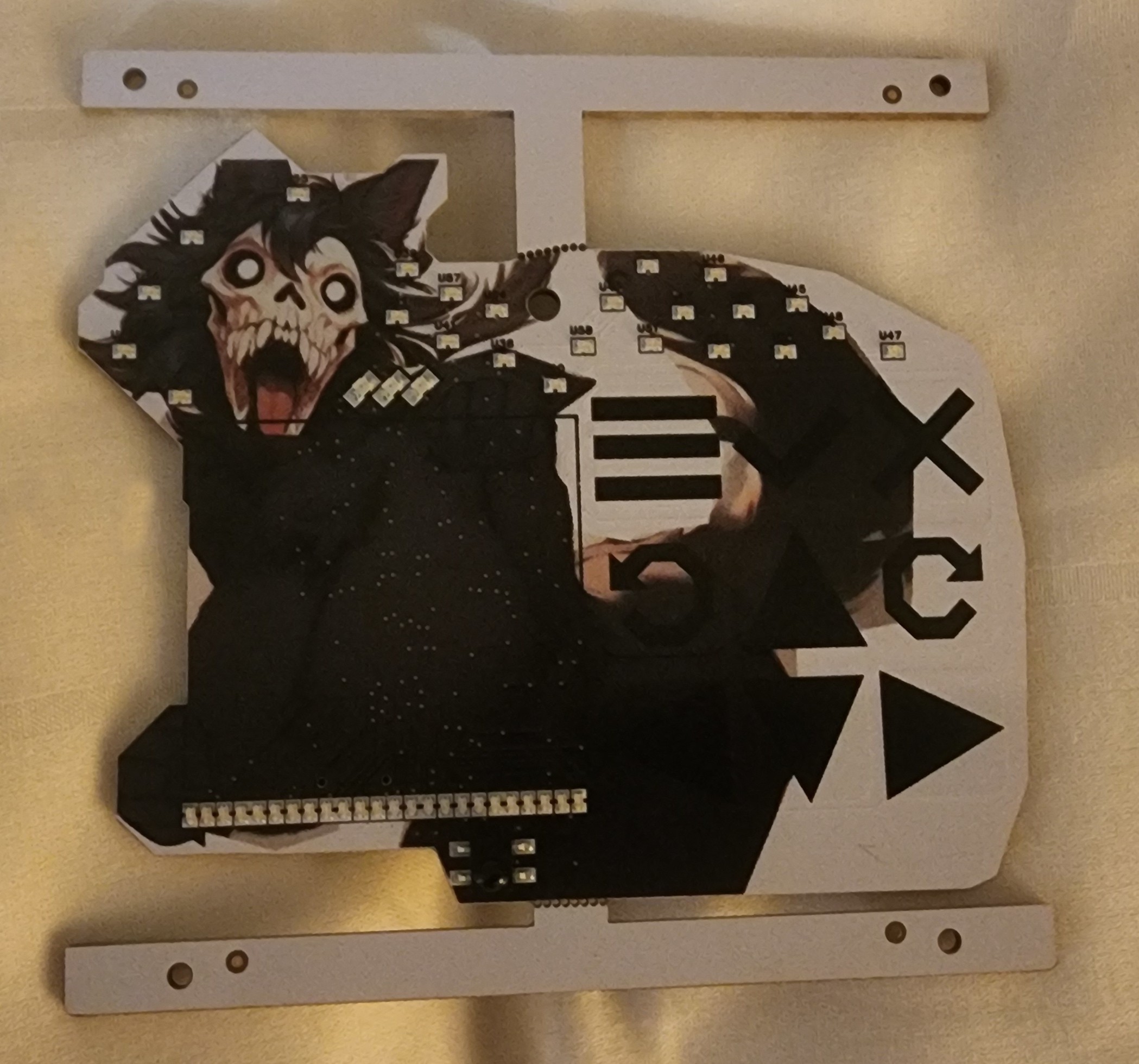
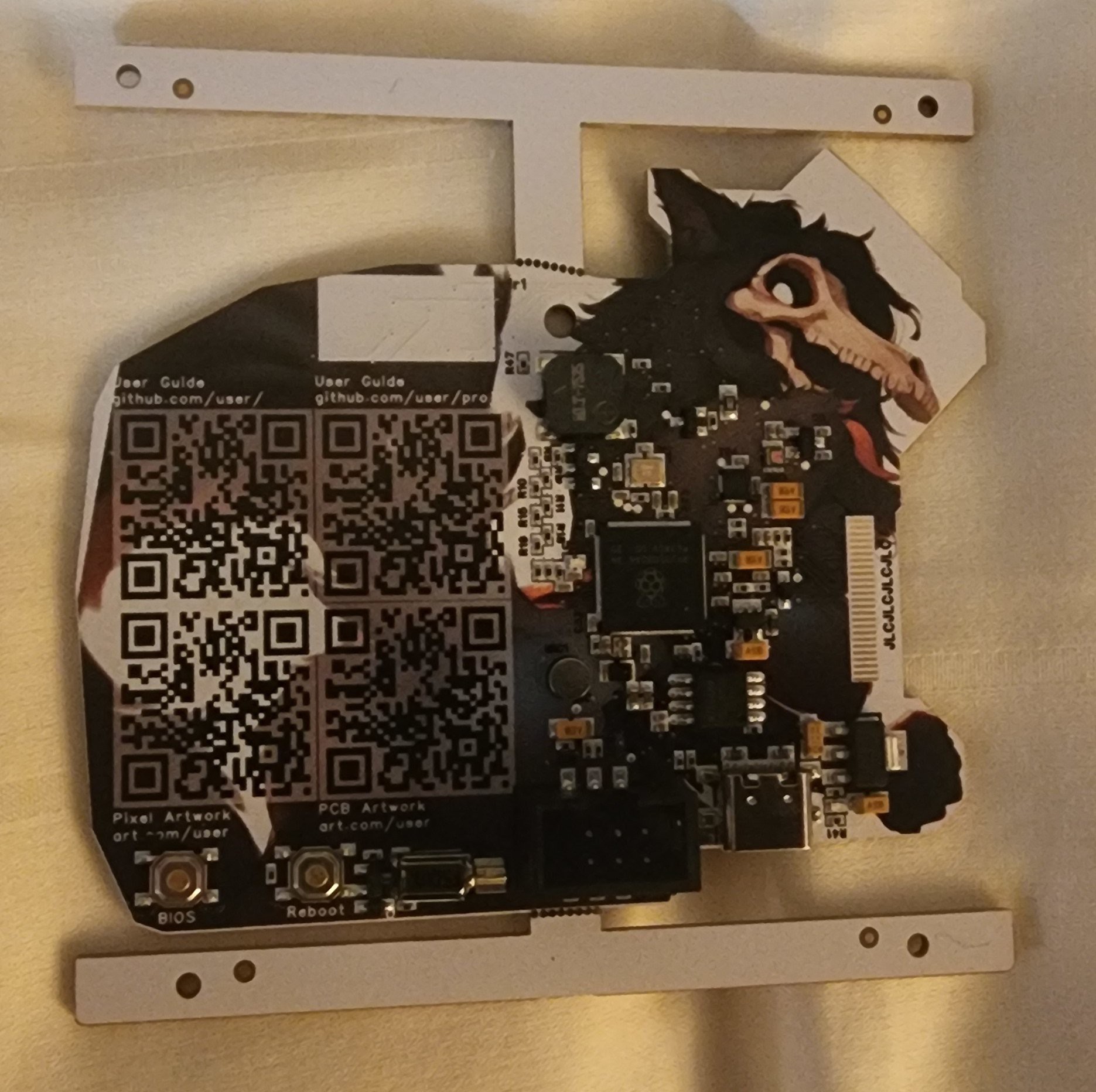
06/21/2026 at 17:09 • 0 commentsFirst action when receiving new boards is to photograph them:
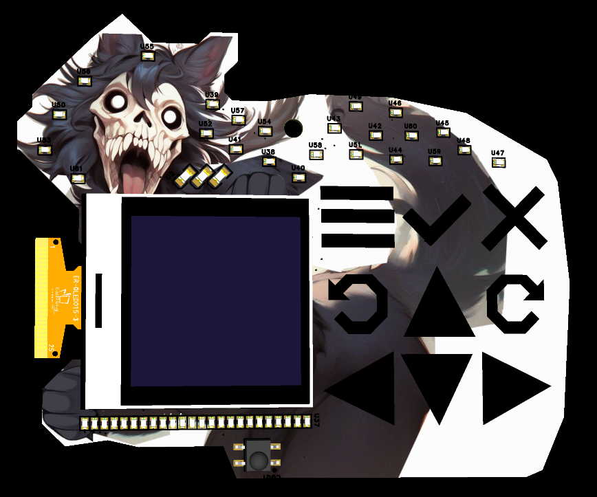
![]()
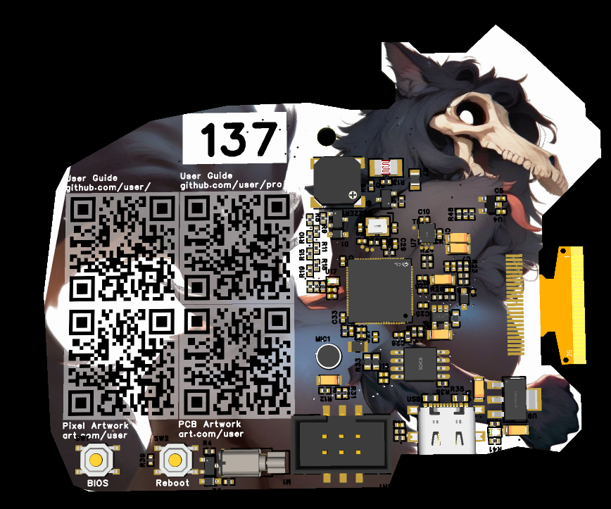
![]()
One detail that irks me is the small white pull-back around every pad. That's a property of the color silkscreen technology, but it's not something you see in the CAD render and does hide/obscure the artwork a little.
I didn't take any effort to remove the black silkscreen, so you can see the reference designators around the entire back side, particularly over the white background
A small note: the fab house has a minimum order of 5 PCBs, but I chose to only have 4 populated with parts - that gives me a clean copy of just the PCB itself that I can check continuity on the traces (workmanship) independent of the parts themselves (ex, a chip may internally close the connection between two VCC pads, where the PCB may have otherwise treated them independently).
First power-ON is the most nerve-racking part of the process in my experience: either the board works fully or it doesn't - it's a very binary fork in the road. It's normally worth taking this step very slowly - I have spare populated prototypes, yes, but those are really for backup/experiments during development).
- Did a resistance check between power (3v3) and ground. Got 600 ohms. Not terribly insightful aside from there at least shouldn't be a dead short between power and ground, so that's good enough to proceed.
- Observed that there is a mechanical interference between the screen and the edge of the PCB (her hand holding the screen). I had specifically planned around this, but still ended up with interference - turns out misread the screen mechanical drawing and though the cable was much longer than it ended up being, so definitely a fix for the next prototype... I later used a dremmel to shave off that part of the PCB so I could assemble the screen properly.
- I applied 3.3V with a 100 mA OCP limit on my power supply, with the thought that if this design was defective, it should hopefully not draw so much power that it destroys itself- trying to preserve the prototypes as long as I can
- The 3.3V power indicator LED came ON (much brighter than I expected, will be decreasing the 1~5mA current draw notably on that LED in the next prototype). Power draw is around 100 mA, where is all that power going...
- Poking my finger around on the PCB to try to find the hot spot, I misdiagnosed the problem as coming from the crystal, and I went down a rabbit hole trying to debug that. In the coming weeks, I would determine it was the neighboring IMU where I swapped the interrupt and VCC pins, putting it in a half-driven configuration that loosely shorted power to ground and drawing excessive power. There is an option to de-solder one part and observe the impact on the power draw that way to definitely prove where the issue is coming from, but I didn't pursue that path here, in part because this is a 2-sided PCB design and makes it hard to rest the board on a hot plate and not inadvertently remove part from both side of the PCB.
- But pushing forward, can it be programmed despite the high power draw? Plugging in via USB in BOOTSEL mode and it successfully manifests as a USB drive just like the pico2 (I was using this for software development up to this point), so far so good. Uploaded a simple blink sketch (driving the debug LEDs), and nothing...
- However, adding in Serial printout works normally, so the chip is running the bit file, but not driving the LEDs... issue was the pico2 is a RP2350A chip, and in order to program the larger (more pins) chip, you need one that enables the extra GPIOs. When I set the Arduino IDE to MyMakers RP2350B, that enabled the extra pins, including the LEDs on the upper bank, and the debug LED blinked.
The objective now is to test each sensor/peripheral to a bare minimum degree necessary to make a go/no-go determination to move forward. Simplest one after the debug LEDs is the motor since it's literally the same code, just running on a different GPIO pin. Here's a "blink" program that ran on the motor for 1 second ON, and 1 second OFF (sounds just like an old school flip phone imho):
Questions/comments/thoughts/requests encouraged
-
Prototype r1 Design
06/20/2026 at 05:00 • 0 commentsOne of the very first risk-reduction activities I did was to inspect how difficult it is to run Python on the Pico2 (RP2350A with 4MB Flash), running across the dual cores. Findings:
- Core0 executes MicroPython out of Flash, which means core1 doesn't have Flash access. Any data that core1 operates on needs to comes from shared memory between core0 and core1 (there is also a FIFO that raises IRQ events, but that's more for flagging transfers than to actually bulk-transfer data)
- I'm not entirely clear how much of a performance hit running Python on a core is vs running C. I opted for C++ code on Core1, accessible as a library in Python in core0. This allowed me to prototype the C code portion standalone in the Arduino IDE (this is the contents of the src/experimentation/ folder)
- The original vision was to have core0 perform administrative functions "draw a rectangle here" and core1 would perform them "pixels x-y in this list are now this value, 'for' loop runs...". Core1 would also handle all the peripherals.
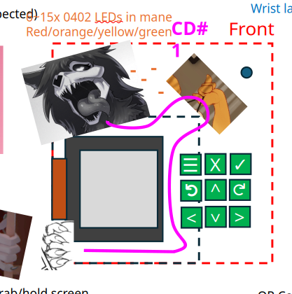
First concept layout
- I had early notions of a leash of LEDs going from her neck all the way around the screen. Later, when I laid this out to scale, the cap touch buttons needed to be so large, there wasn't good clearance between the touch pads on the right and the screen on the left (plus I has EMI/EMC concerns between the sensitive cap touch pads and the high frequency charlieplexed LEDs), so I ultimately broke this string of LEDs into two banks: one in her hair, and one as a kind of status/scroll bar below the screen - giving the cap touch pads a clan shot directly into the processor (where I'm trying to measure capacitance changes on the order of 10s of pF).
![]()
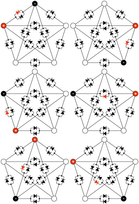
- I opted for red-green LEDs, on the premise the primary color of SCP content is a shade of orange (mix of green and red). Chareliplexing N pins allows control of N*(N-1) LEDs - ex for 8 pins that's 56 LED elements. The width of the screen fit around 24 LEDs (24 red-green LEDs is 48 LED elements). So I moved forward with a lower bank of 24 red-green LEDs below the screen, and an upper bank of also 24 LEDs. This allowed me to recycle the same PIO/code interface between the LED banks.
- I considered WS2812 LEDs to get full RGB support (also called "NeoPixel"s by Adafruit). The SAO standard stipulates 3.3V input, and I disliked the idea of needing to add a 5V step-up converter required by the WS2812s. I wanted to keep the BOM cost reasonable, so opted for dumb LEDs (with a 1.8~2.3V forward voltage) with a plan to Charlieplex them (requires floating most of the GPIO pins in a bank, and then driving one pin high, one pin low, holding that for a tiny fraction of a second, then moving on to the next pairing). The RP2350 supports floating the pins through PIO, where the prior generation chip did not. The impact of chareliplexing LEDs vs a serial string of WS2812 is that it notably complicates PCB layout since there is now a direct electrical connection from LED directly to the processor (vs just a chain connection to each LED's neighbor in WS2812).
![]()
- Those reviewing this closely will note the processor runs at nominally 3.3V (per the SAO standard), but the green LEDs wants ~2.9V and the red ~2.1V. There is a dirty trick where high current draw (~20mA) through the processor will actually drop the drive voltage a bit, so I actually drive the green LEDs straight off the RP2350 GPIO pins. For the red, I did include a resistor dropper, but I kept it to only 3 resistors total across the entire bank of 8 GPIO pins. I did this by carefully selecting grouping of red LEDs to all share a common pin and routed the red connections through the resistor before reaching that gpio pin.
- All this work was done before the DEFCON34 MICD was released. At this stage, I was very concerned about overall size and keep-out zones. Most SAOs gravitate to around 2~2.5" max outer dimensions, but this quickly expanded past 3". I also assumed that the major keep-out zone would be below the SAO, so I worked to keep the PCB real estate south of the SAO as limited as possible
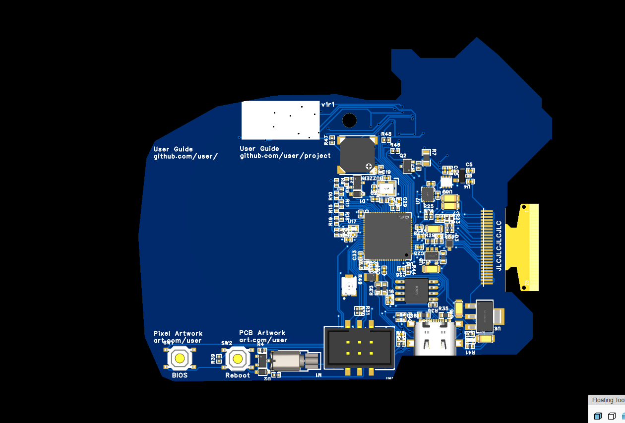
- I wanted to keep the design elegant, and my definition of that is as few holes showing through the board as possible (really want to highlight the final artwork as much as possible). I opted for a USB-C port where I could hide the structural holes behind the screen. I also had a surface mount SAO header on this prototype.![]()
![]()
- I've been told it's wise to give each PCB a serial number. JLCPCB now does this automatically for you if you want, but only for standard silkscreen (cannot be selected for RGB silkscreen I'm using here). So the fall-back option is a big white square where the serial numebr can be hand-written in.
- The area behind the cap touch keys needs to be devoid of parts to avoid coupling interfering with the measurements. This naturally paired with QR codes. I had a notion of a link to the Github user guide, and to the two artists I'm working with (one for PCB/sticker artwork, one for pixel artwork). However, per some user feedback, later revisions simplified this to a single gihub.io splash page that has several links off from there.
- There's an inherent chicken-and-egg dynamic between the layout and PCB artwork. To try to decouple that, I opted to just use a generic AI generation on this first prototype.
- Cap touch to me seemed the biggest risk, so I actually tried two different routings on this first prototype: the main set of 9 buttons have a 1 MOhm resistor to ground. To take a measurement, the PIO pin is tied to 3.3V, then floated, then the pins are read/polled until they schmitt trigger below the cut-off voltage to read as a '0'. This is a hacky way of measuring the decay constant of an RC circuit. It should also be noted this only works on the A3/A4 stepping of the RP2350. If you have a Pico2 with "A2" at the end of the chip name on the board, then erratta E9 applies where there is a relatively huge current leak on the GPIO pins, making cap touch (and anything less than ~8 kOhm pull up/down) not work on those models of chips.
- The super secret super snooper booper button (spoilers) I routed differently, replacing the ground connection with a PWM pin. In this way, I can set the PWM to toggle at a constant rate and leave the cap touch pins as constant high-impedance inputs (just polling for 1/0 state changes) - just looking at how long it takes for them to change state relative to the PWM pin. This saves me from having to toggle between modes with the PIO assembly instructions.
- Eccentric vibrating mass aka vibration motor I setup so it's pointed at the SAO header on the hopes that if it's shielded on two sides (motor housing and SAO header) it's a little less likely to get caught up in fabric the user is wearing.
- The photo-resistor was a late removal. I show it here on the prototype as I submitted it, but the fab house flagged it as something they'd have to drop their reflow temperatures to comply with (ie. the part is designed for leaded reflow temperatures, but China generally uses unleaded, which is ~30 C hotter). Rather than paying a bunch extra to process the board as I originally designed it, I swapped it out for an I2C photosensor for the final submission.
![]()
- Layout itself went relatively smoothly (I'm quite fond of how the chareliplexed LED lines all go up in parallel together North of the processor). The rat's nest had something like 300+ connections that it took me a week or two (working in the evenings and weekends) to connect. The real trick is planning out which parts will go to each GPIO pin so they can be organized radially in that order. There's something about the RP2350 I'd call "academic" where the design decisions seems very clean and symmetric. Most processors will have 4~8 functions each pin can perform and there's a calculus to figure out which ones can be assigned to which peripheral. The RP2350 seems more relaxed in that regard where virtually everything can go to almost any pin (to the point I had some analysis paralysis where many peripherals could go to many pins). There are some constraints, like all the analog pins have to be next to the USB since that's the only ones plumbed for analog input. Any pins being driven by PIO should all be grouped in a uniformly-increasing sequence together since that's how the PIO expects to update them. There are only two SPI and two I2C hard IPs (yes, the PIOs can mimic that to an extent, but it's extra complexity) - so it's important to track which sensors are on the i2c0 line vs the SAO i2c1 line. A late find is that if you want to drive PWM on pins, you'll want to track which bank each pin is on - neighboring pins are often on the same PWM port and must be driven at the same frequency (useful for H-bridge control on motors but not applicable here).
- Every PCB layout seems to have a bottleneck of some kind - something where you can show a closed form solution that stacking up all the design rules means that two parts can only be so close, or there can only be so many electrical connections between point A and B before you max out the width of the circuit board. In this case, the LEDs below the OLED were the tightest part of the design, requiring multiple passes and tweaks ebfore I got them all to fit.
Questions/comments/thoughts/requests encouraged
-
Getting Started - Project Formulation
06/18/2026 at 07:56 • 0 commentsThe idea for this project came together while walking around Supercon 2025 and combining several factors:
- I made made an SAO design for DEFCON31. I had a base design that could be customized with a sticker. One lesson learned was that scrounging through a bag to find the exact right sticker the customer wanted was time-consuming. Rather than many products offered at a single price point, it's better to diversify the product offering across price points, or just offer a single configuration of the product. Also, the dark/broody design sold the best (and incidentally was the one I made the least copies of and sold out first).
- DEFCON is themed around skulls and hacking
- If centering the design around a character, it would be advantageous to avoid copyright (ie. open source character), but still have something recognizable. This being for DEFCON34, could have a tie in with rule34... (but still keep the hardware and software design formally SFW)
- A rock-paper-scissors type interaction is very effective as an ice breaker, but lacks motivation to continue talking with the person after the first interaction. Want something with more staying power, like a chat bot that is broadcasting messages/replies - so the longer you talk with someone (assuming both have this SAO), the more of their messages you pickup, and maybe unlock perks in the SAO... (FYI, laser tag has been done)
- Have had requests in the past to make the SAO hackable, so want something modern running at least some Python, so thinking RP2040 or ESP32 product line for good community support. Went with RP2350B and 16MB external Flash.
- I've had trouble conveying information (game/menu state) to users with LEDs alone, so want to include a proper screen in this design so information is all presented in one place.
- I wanted to do capacitive touch buttons since they are the lowest profile option and feel better (imho) than traditional clicky buttons. ESP32 has a built-in controller for this, but the RP2 series does not. So doing capacitive touch on the RP2 series will be a gamble/risk... Since most are right handed, would have the buttons on the right, and the screen to the left.