 Luis Mestre
-
How everything actually works
10/17/2026 at 08:52 • 0 commentsI've put some cool results down but I haven't really explained what I am doing and what's actually happening on the electronics side. Software is something I'll get into in a later post. There are still things I'm not happy about on the electronics side so I'm mostly going to document the electronics through block diagrams at the moment. Once the new design is finished, I'll document this. As it stands the PCB needs some improvements like ESD protection, overcurrent and voltage protection etc, it works fine but it's missing the good practice things that people like me are always lazy to add in addition to the actual connection mistakes I made. I want something that can just be ordered from JLCPCB, plugged in and it works and can be ordered for years. This means no electrolytic caps, old components etc. The project as it stands from a hobbyist's perspective is effectively finished but I would like to turn this into a product kit perhaps so I will continue to improve it.
Ok that aside, so how does an AFM work from the signal processing point of view. The heart and soul of the digital signal processing chain, is a lockin amplifier. I assume nerds like me on here know what this is but without going in too deeply, it's just some magic maths that just produces the amplitude of a sine wave at one frequency which is the frequency you are driving the tuning fork with the 32kHz signal. If you want to dig into how this works, this page has a great explanation https://www.zhinst.com/ch/en/resources/principles-of-lock-in-detection/. The other frequencies like 50Hz noise etc are magically filtered out. It effectively turns the signal of a sinewave into DC, this now means you can oversample and integrate the hell out of it which kind of magically turns my crappy 12bit ENOB STM32h7 ("16bit ADC", which is not actually 16 bit) into something with way more effective bits. You can think of it as oversampling a DC signal.
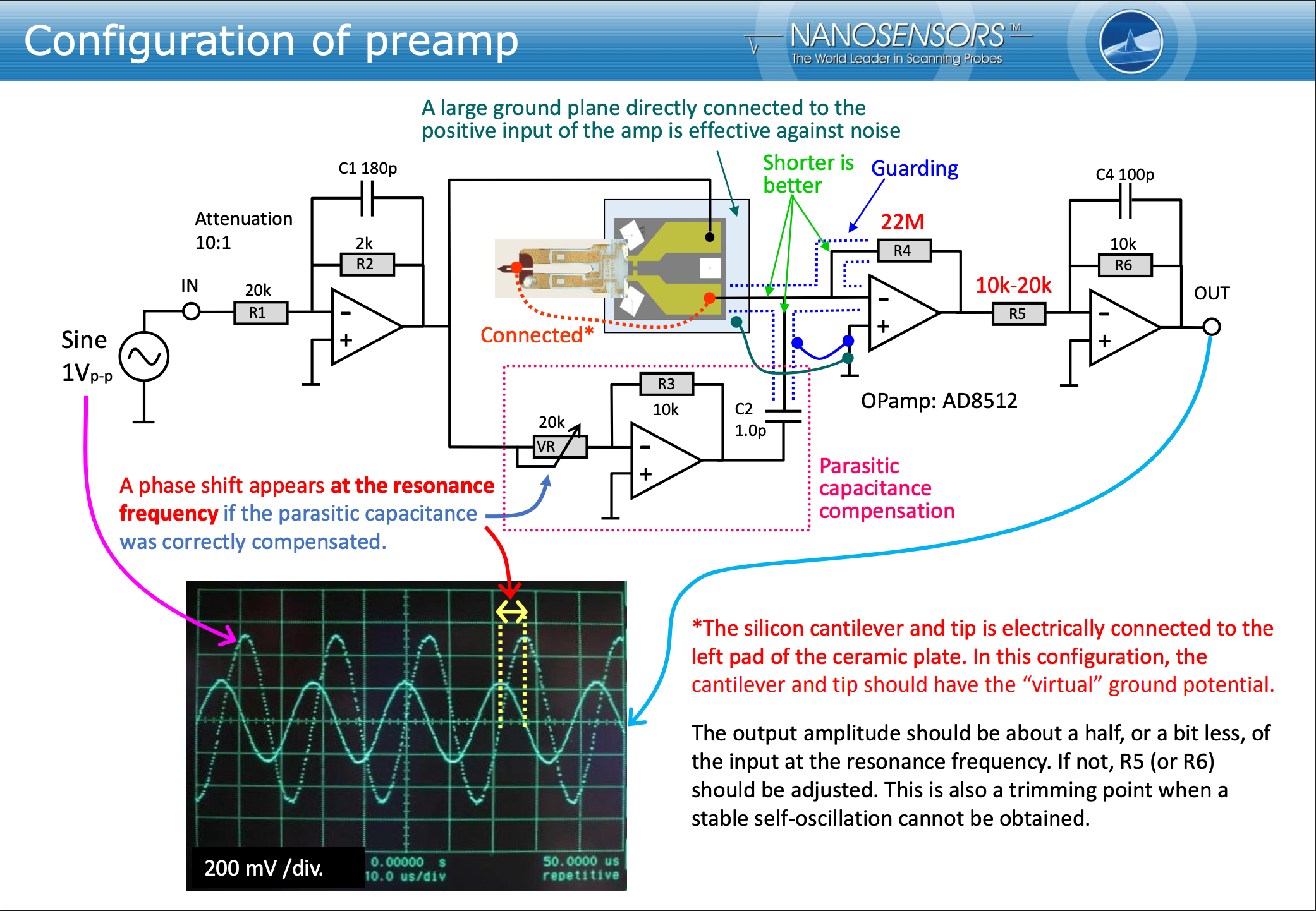
The current signal from the tuning fork is very tiny and we need a current to voltage converter. This circuit is called a transimpedance amplifier. The problem with tuning forks is that then have parasitic capacitance and therefore some of the drive signal used to drive the tuning fork actually goes through the tuning fork itself and interferes with the piezo electric signal from the tuning fork this means depending on the cable length and even the type of tuning fork you can get what looks like an antiresonance where the tuning fork is resonating. This is described in the akiyama documentation here https://www.akiyamaprobe.com/AKIYAMA-PROBE_SimpleContoller_v2.pdf . Therefore, one needs a transimpedance amplifier with an extra signal path that inverts the drive signal, attenuates it to the correct amount and then adds it to the signal out of the tuning fork. This is exactly what Akiyama's circuit does which is shown below.
![]()
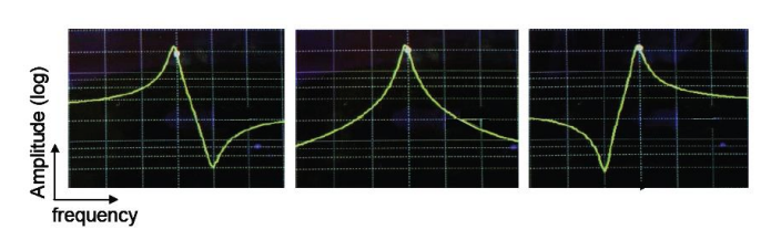
Akiyama's TIA design The circuit is tuned by adjusting the 20k potentiometer which just controls the amplitude of the inverted drive signal to perfectly cancel out the signal that passes through the parasitic capacitor. I already tuned my circuit to have a nice curve and didn't want to detune it to get this data as it's in the documentation. A screenshot of the documentation is below but I really recommend if you are interested that you read it from the link above it's very useful.
![]()
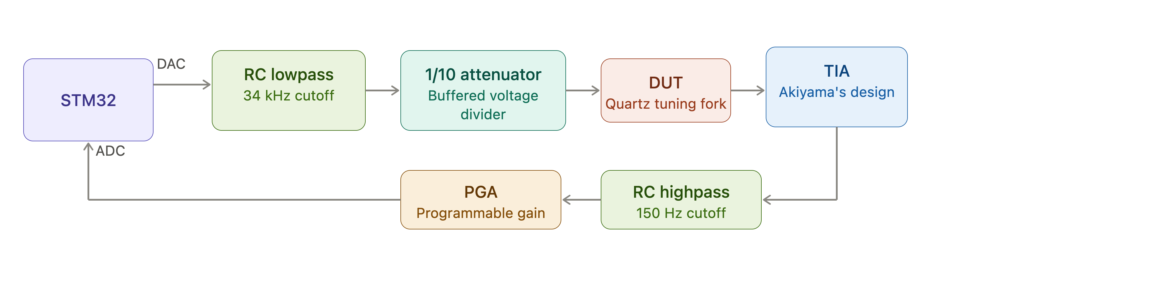
how the frequency sweep look untuned and tuned With this in mind, my signal chain is as follows below.
![]()
Signal chain The LPF cuts off the higher frequency stuff from the STM's 12bit DAC that is used to generate my drive sinewave and the HPF before the PGA is used to cut off 50Hz harmonics (I will make this a 1kHz or 10kHz cutoff as even my overloaded DIY tuning forks tips only go as low as 23kHz)
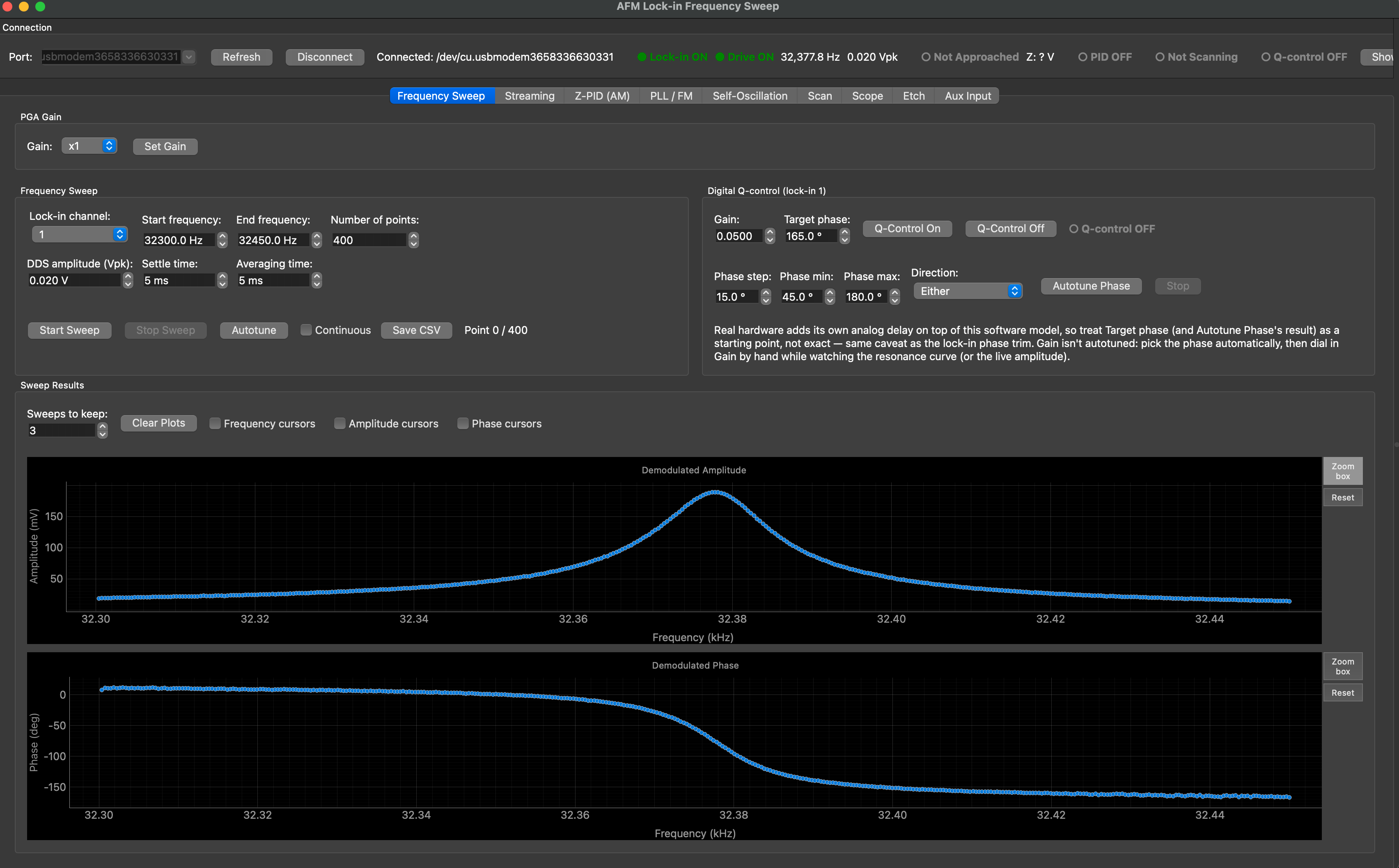
After tuning and doing this signal chain, I get a frequency curve like this.
![]()
Example of frequency sweep result with my setup Worth mentioning the drive amplitude of 20mv is before the 1/10 attenuator is what they use in my lab for the same tips. This is a pretty clean resonance on the same level as what comes out of the MFLI Zurich instruments 5k lockins we have in my lab. The reason is that most of the noise in this circuit comes from the massive 22Mohm feedback resistor in the transimpedance amplifier so there is not much point in having a very precise ADC especially with lockin amplification and this is why the crappy DAC and ADC from the STM32's peripherals work perfectly fine here. The software DDS signal from the STM's DAC gets low pass filtered in my circuit and then bandpass filtered by the tuning fork itself, in fact you can drive the tuning fork with a square wave most of the harmonics get filtered out anyways it really doesn't care much especially if the Q factor is high enough.
-
Current sub nm Z resolution
10/13/2026 at 10:17 • 0 commentsI will just put some Gwyddion analysis of calibrated images on here. I recently used a defective power supply to power my working board and unfortunately it went up in magic smoke. I still have another working board I am using to debug noise in the transimpedance amplifier but I have no DAC to scan with my stage. Since I will redesign it anyways to add things like overvoltage and current protection, ESD etc, I will mostly put some analysis things on here now while I redesign the board (might take some months...). Currently I am using a piezo buzzer with a rough 14um range with a 16bit DAC. The resolution I obtained in the Z axis is on the order of 200 picometers (pm) or which turns out to be roughly the DAC step. This makes sense as when the PID is well tuned one can really see individual DAC steps into the piezo on my GUI. An easy way to increase this resolution is to use a lower range piezo with the same DAC eg have two gain settings for the DAC buffer (something else I will implement in the new board). This would allow one to have a resolution to look at tiny features like atomic steps (with reduced Z axis range) and then bigger features (with larger Z range).
Disclaimer:
These "z-resolution measurements" are very order of magnitude hand wavy checks. I assume that in the flatter parts of the image this is my electrical noise. In reality I am also seeing surface roughness I am assuming my calibration grid is mostly atomically flat over small enough regions where there are no clear vibrations affecting the measrument which is probably not true. So I am seeing a mix of noise and surface roughness. Therefore, I would argue my noise can actually be a bit lower. I don't have access to mica samples at the moment and since the board blew this will have to be another test. However, to add to this, with a proper grounded enclosure however, I have noticed I have much lower noise so the future resolution of this microscope will likely be in the 10s of pm range when everything is fully finished and optimized.
I noticed
This seems to be reproducible across images. At some point I tried cleaning the AFM grid with some IPA in my lab which was very dirty and now the grid looks like this until I take it into the cleanroom and dip it into some piranha solution. But one can still see sub nm resolution. worth mentioning, this is with two different tuning fork tips one is the commercial one I got from my lab for free which is the one below and the one above is my DIY tip. My DIY tips actually behave much better with easier PID tuning since they are tapping mode rather than shear mode but when well tuned the shear mode one can also provide good images. On the image below I also changed the piezo preload on the stage and it's not quite as good as the previous that I will go back to so bear that in mind but this is just a rough resolution estimate exercise.
![]() I noticed the current resolution is dependent on both electrical noise floor and PID settings but it's far more dependent on PID settings as the PID can be tuned well even with a noisy signal, and the topography scans can look clean despite the amplitude scans looking quite dirty. Electrical noise seems to be mostly dependent on the shielding of my transimpedance amplifier and cables leading to the tuning fork more than the stm32's ADC and I will at some point document these tests here. As I found out I am mostly limited by Jonhson noise of the feedback resistor and other random factors meaning there is no point in getting a better ADC than the STM32's 12bit ENOB one which already gets me subnm resolution and comes within the very cheap microcontroller instead of an expensive external one.
-
DIY tips working
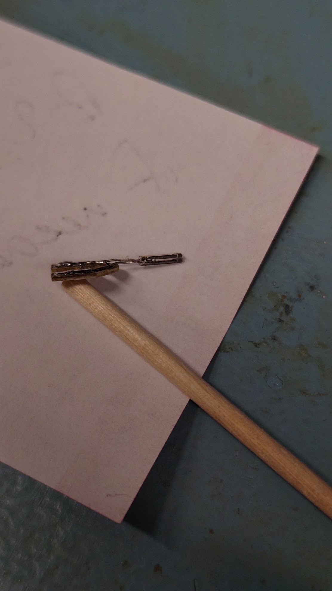
09/26/2026 at 14:12 • 0 commentsI have now managed to get the tip making process working and it takes me about 20 min to make a tip from scratch. Usually with DIY or even professional AFMs, one would have to buy the cantilevers as is the case with the famous DVD optical pickup unit AFM by Prof. Edwin Hwu. With professional quartz tuning fork AFMs Akiyama tips are the standard but these cost around 80 dollars per tip. The tips I will outline here have a cost of cents in materials. The only thing needed are standard tuning forks and tungsten wire. A bag of 100 tuning forks can be had for a couple of dollars and 1-2 m of tungsten wire is around the same cost. I believe any thickness works and the thinner the better to prevent loading of the tuning fork and thus a decrease in its Q factor which will lead to worse sensitivity. This being said, I have used 250um because I had it laying around and it's easy to handle and it works great even the low Q factor tuning fork is sensitive enough. Therefore, this means the AFM is fully DIY now including the tips. Below is an example tip made using the method I will outline.
![]()
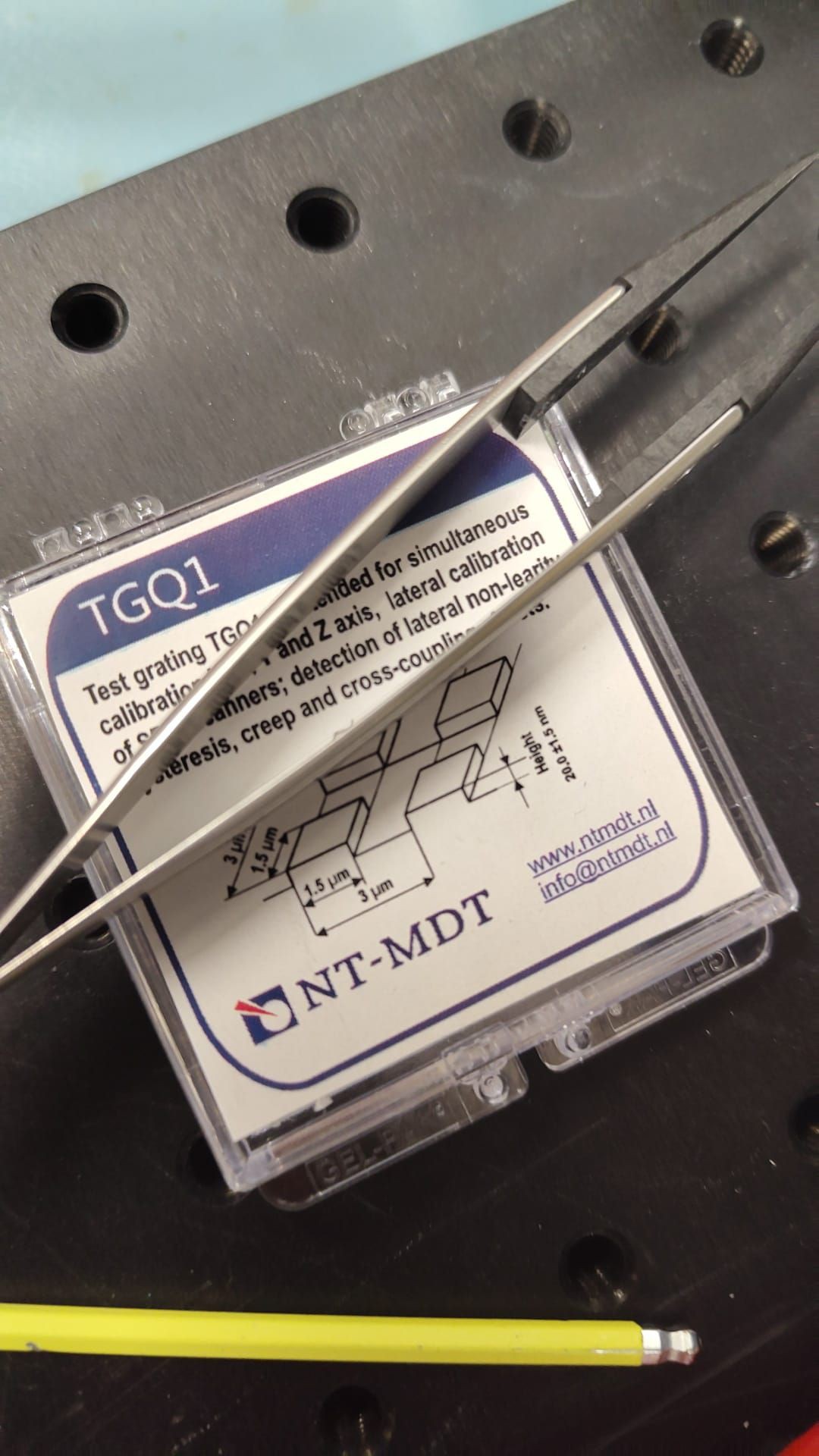
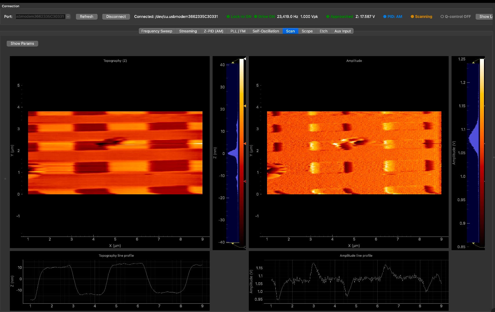
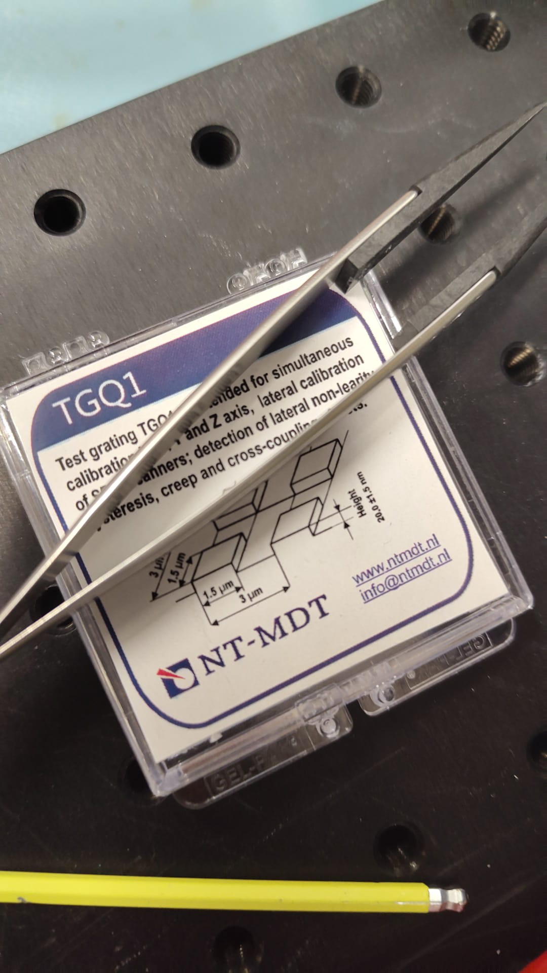
Images taken with this tip loop very good. I have since implemented a scan that takes the forwards and backwards scans and separates them into separate images to more or less eliminate the hysteresis which was causing the previous comb line artefacts. Here is an example of a forward scan image of a 1.5 x 1.5 um and 20nm high square AFM calibration rating, the result looks very similar to our AFM in house 3D printed stage distortions aside. I repeat 20 nanometers!! This is a screenshot from my GUI also showing the amplitude image, I also have the pose image it's just not shown here. The phase gives you interesting information about surface properties due to dissipation do it can be thought of as some sort of friction due to viscoelastic effects (e.g. water layers on the surface). You can see the noise level is basically in the single nm level (I need to enclose the AFM to get better than this as I think I am limited by some environmental vibrations).
![]()
AFM grid imaged here ![]()
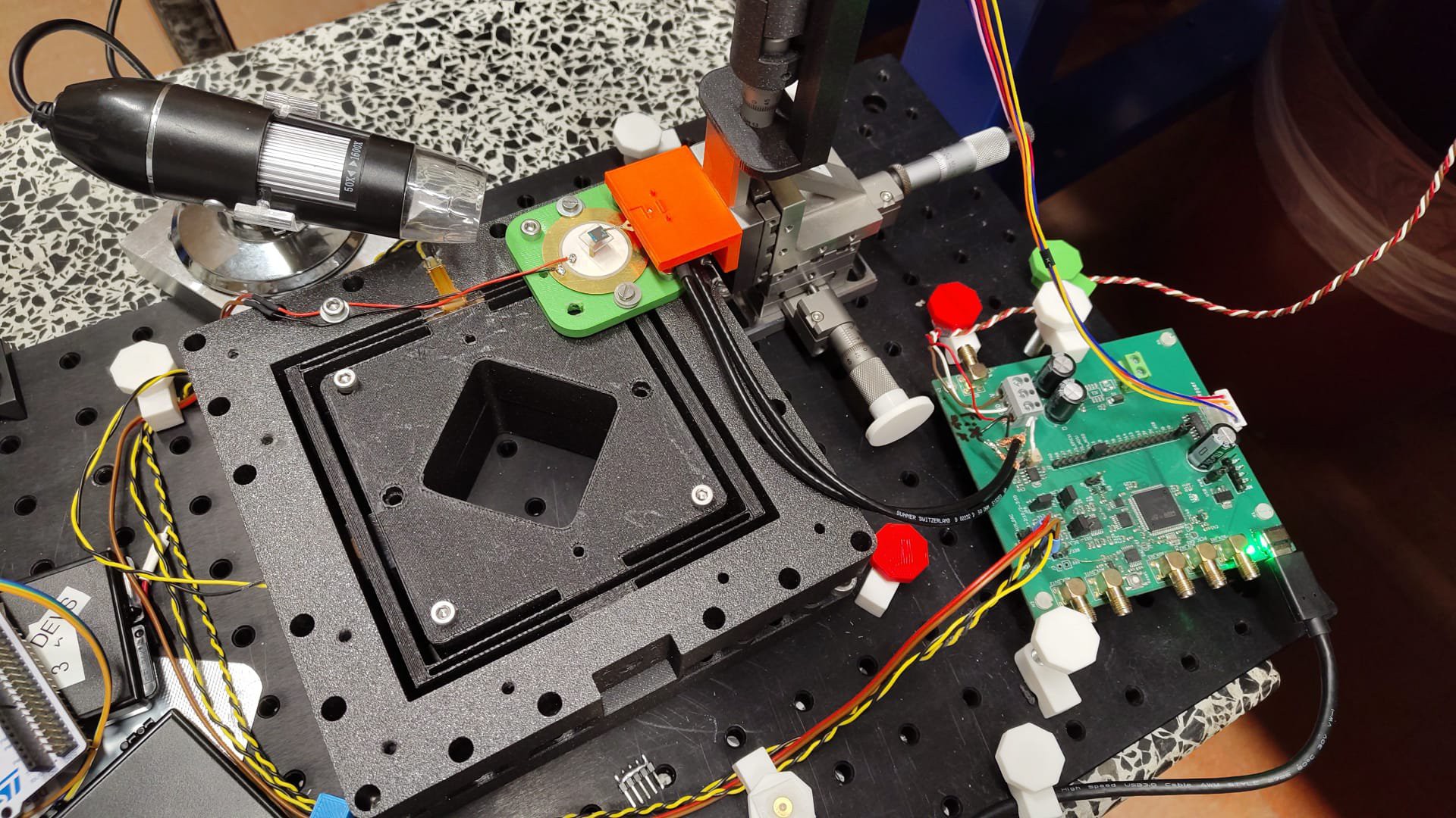
image of calibration grid with tip The setup looks like this. Black 3D printed flexure stage, um stage holding the tuning fork with the driving shielded black wires and this sits on top of a granite slab that sits on top of you guess it a bike inner tube for damping. the um stage is for moving the tip in x and y, and the z is motorised of the auto approach which is now also working great. the PCB is my control board and the start of the show it does the digital lockin, stage driving, tuning fork amplifying etc.
![]()
current janky setup Tip making process: For this one has to start by decamping a standard tuning fork 32768kHz resonator. The look like this

Vacuum encased off-the-shelf tuning forks
These are easily recapped with some care. I take a pair of flat pliers then around where the wires are coming off, squeeze carefully until I hear a little crack, this is the resin for the vacuum encasing of the tuning forks. I then go around with the pliers until the resins is fully cracked and and then the tuning fork just pulls out. The tuning fork connections to the wires are very fragile when the tuning fork is out therefore I usually solder this to a little PCB I have but you can use any holder just make sure to do major handling while the tuning fork is encased to prevent breaking the connections, I learned this the hard way...The tuning forks then look like this soldered to a PCB to hold them
![]()
Decapped tuning fork.
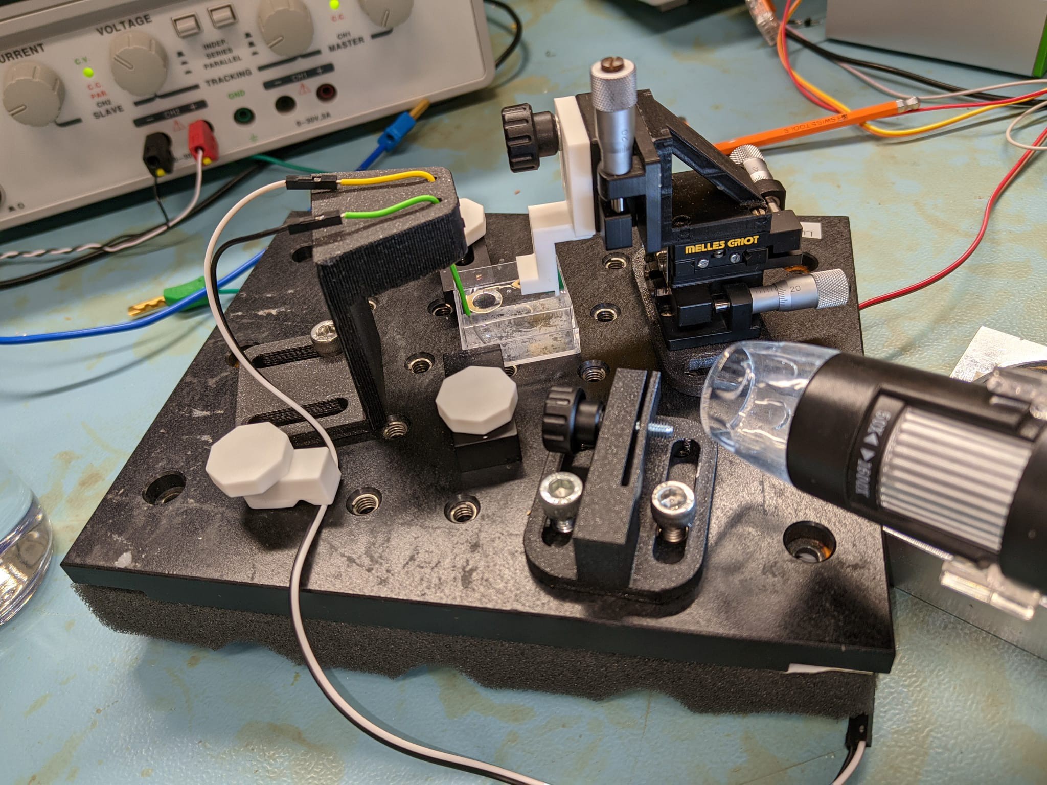
Then comes the gluing of the wire to the tuning fork and the etching. For these I made this little tip making station. the tip making method is based on the mad city labs method https://www.youtube.com/watch?v=K_k5UsHlwN4. Note the foam under the mini scrap optics breadboard (also from the bins haha) This helps immensely with vibration damping during the etch which is important to keep the tips consistent as you don't want the meniscus to move during the etch.
![]()
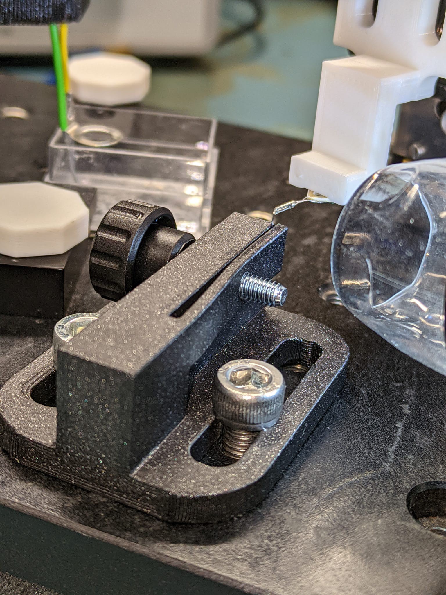
This station goes the dip gluing and etching by rotating the micrometer stage between the two positions. I am using this stage because I got them for free from the bins at my university but one can 3D print these there are some models online if you google 3D printed linear stage or just buy some mini stages from aliexpress, they are about 60 for the 3 axis If you look enough. This doesn't require much precision so you can literally make something with normal screws.
![]()
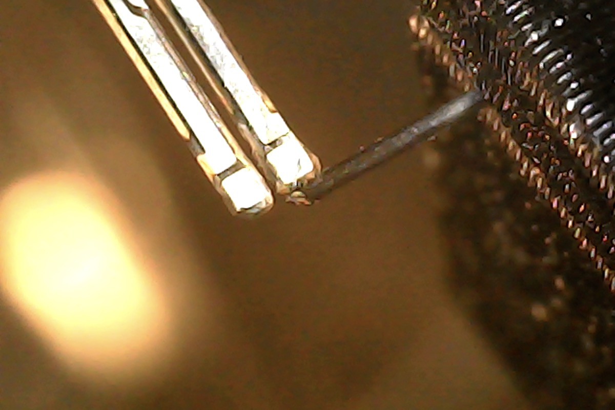
I first add a dab of standard superglue on the bottoming of the fork you have to be careful not to bridge both tongs, you can use the stage by using the holder clips to hold some sharp needle with glue but I just do this by hand. I use a USB microscope to check this and it should look like the picture below.
![]()
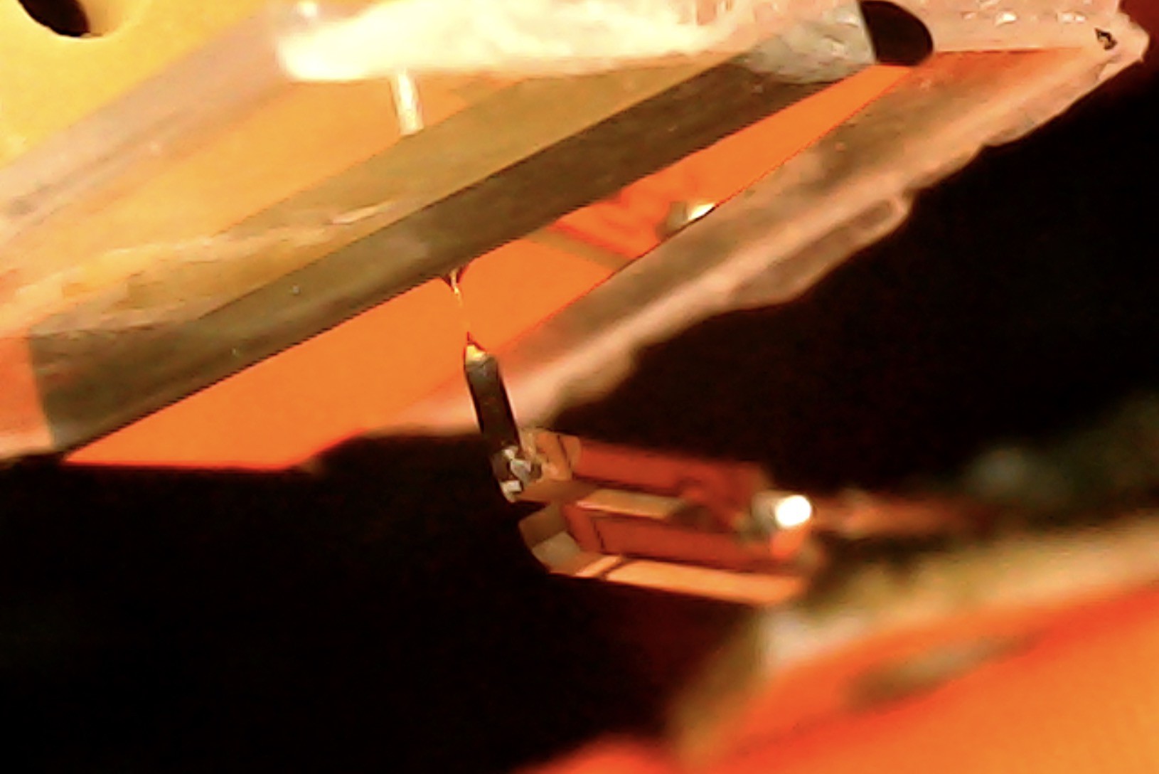
I then etch the wire in 4M NaOH solution, you can get this from drain pipe cleaner usually but I was able to get some actual NaOH and made my own solution, you should be able to buy this chemical relatively easily online. Etching can be done using the lamella method and 5V just like in the mad city labs tutorial. 4M seems to work well for 250um tungsten wire but if you use thinner wire you might have to use a lower voltage/NaOH concentration. you have two electrodes, one is the green wire and the other is the ring. I usually fill the little tank until the ring makes a little bubble then I remove some NaOH solution leaving the ring bubble. I then move the tuning fork with the wire into it and make sure the bottom of the tuning fork wire touches the liquid below the ring. I then add a little drop to reinforce the ring bubble. Finally, I add the 5V. I use an H-bridge to reverse the polarity a couple of times at the beginning of the etch to follow mad city labs but you can just use DC and it works. The ring must be the negative terminal (cathode) you can tell as the bubbles will come from the ring and not the wire in the ring. After about 10 min the wire will drop but you should see it etch like the picture below where you see the sharp tip of the bottom wire.
![]() At this point you should have a tip that works, the full process with this nice little etching station takes about 20 min I don't really wait 24 hours like the mad city labs tutorial says to, I make them and scan right away and it works fine.
![]()
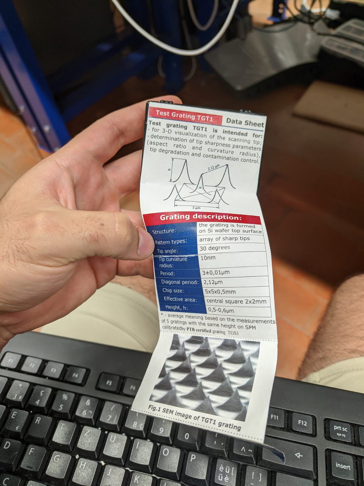
Caveats, I have not yet measured the radius of the tips, I don't have easy access to an SEM and will have to come up with something as the SEMs we have are in the cleanroom and I don't want to waste group money on personal projects. Since everything you measure is tip convolution with the shape, you can just use a grid like the one I presented to before with the spiky things to characterise this although if the tips have a low aspect ratio this might not be very accurate so I will work on this.
Another thing to note is that this drops the frequency and Q factor of the tuning fork by quite a bit. After this wire is attached, the new resonance is around 23kHz for these tuning forks rather than 32768Hz and the Q factor also drops a lot. I just realised I didn't record the frequency sweep so I will add it later and compare it to an enclosed tuning fork. I usually just run autotune and it automatically fine the frequency to drive it at. All this being said, it still works great and there are papers where they add a wire to the other fork tong to match the mass and preserve the Q factor but this works fine and I was too lazy.
Things to come.
- Get PLL working for frequency modulated AFM, I have it implemented but it's hard to tune and I haven't figured the parameters yet, this will likely allow me to scan a bit faster since I don't need to wait for the tuning fork to ringdown since frequency shifts are instantaneous.
- Work on a flexure voice coil stage. Nanosurf uses this for their educational system AFM and for large range nm resolution it might be interesting as it does not have hysteresis and if well designed it should be linear and nicer to run in open loop. nm resolution is fine for most things and without vacuum seeing atoms with AFM is hard anyway.
- Images of things that are actually cool since now the system is more or less optimised and really usable.
- At some point I will explain how everything works once I am happy with the final state of the project since I am still optimising and I am not great at writing things up.
-
Current state of the project
08/19/2026 at 09:19 • 0 commentsCurrent state of the project is that it is working and rather well. I actually had a look on hackaday and there seem to be other quartz tuning fork AFMs going but no one seems to have gotten nice images. I am fortunate enough to be in the right scientific environment for my work where I can ask people questions when I get stuck and therefore I wanted to put this project on here to perhaps show the other projects is doable and for them to take some ideas out of this was well. I am not sure how much time I will have to document this very throughly especially because I am still improving the setup and want to do this once it's in its final state but I hope it's useful to someone. I want to make a little kit people can buy and just assemble for university labs and hobbyists but I will also work on 3D printed stages anyone can build at home with some time which should be dirt cheap and these I will try to put on here in more detail. The PCB etc I will document at the end once I am happy with it's final state as this was my first iteration and still needs improving.
Now for the cool stuff. The images shown are from AFM calibration grids one has steps of 20nm which really require a decent AFM to see. I also tried to image a graphene device with some wires coming out. Bigger calibration grid is quite easy to see. Some examples of images are below
![]()
This is the image below
![]()
as you can see the forwards and backwards scans during the raster scan have different sizes (the backwards scan is stretched in comparison with the forwards one) I believe this is the piezo hysteresis in the stage. This is fixed by scanning in a single direction. That is, once you reach the end of the forwards scan, you lift the tip move it back reengage the PID and scan again, this unfortunately adds some time to the scan but fixes this issue more or less.
New images I took are now with improved noise from shielding on the tuning fork wires leading to the transimpedance amplifier (TIA) and below you can see a 20nm step from the calibration grid with 20nm high 1.5um wide squares
![]() Here is an example of the 20nm step with improved noise. The previous steps looked like this:
![]() With the improved shielding on the tuning fork wires to the TIA the same 20nm step is much cleaner. I believe now I am limited by environmental vibrations due to my damping being a bike inner tube, to see atomic layers, I likely need and enclosure and the setup suspended by springs with eddy current damping from magnets similar to Dan Berard's STM. but I would say this is pretty good already for most applications like looking at cells or DNA.
![]() I also imaged the connections wires to a graphene device kindly given to me by a friend where you can see 10s of nm high wires, It's a little hard to see in the topography image without better processing in gwyddion but you can see the e-beam evaporated gold wires coming out from the graphene flake in the amplitude scan quite well.
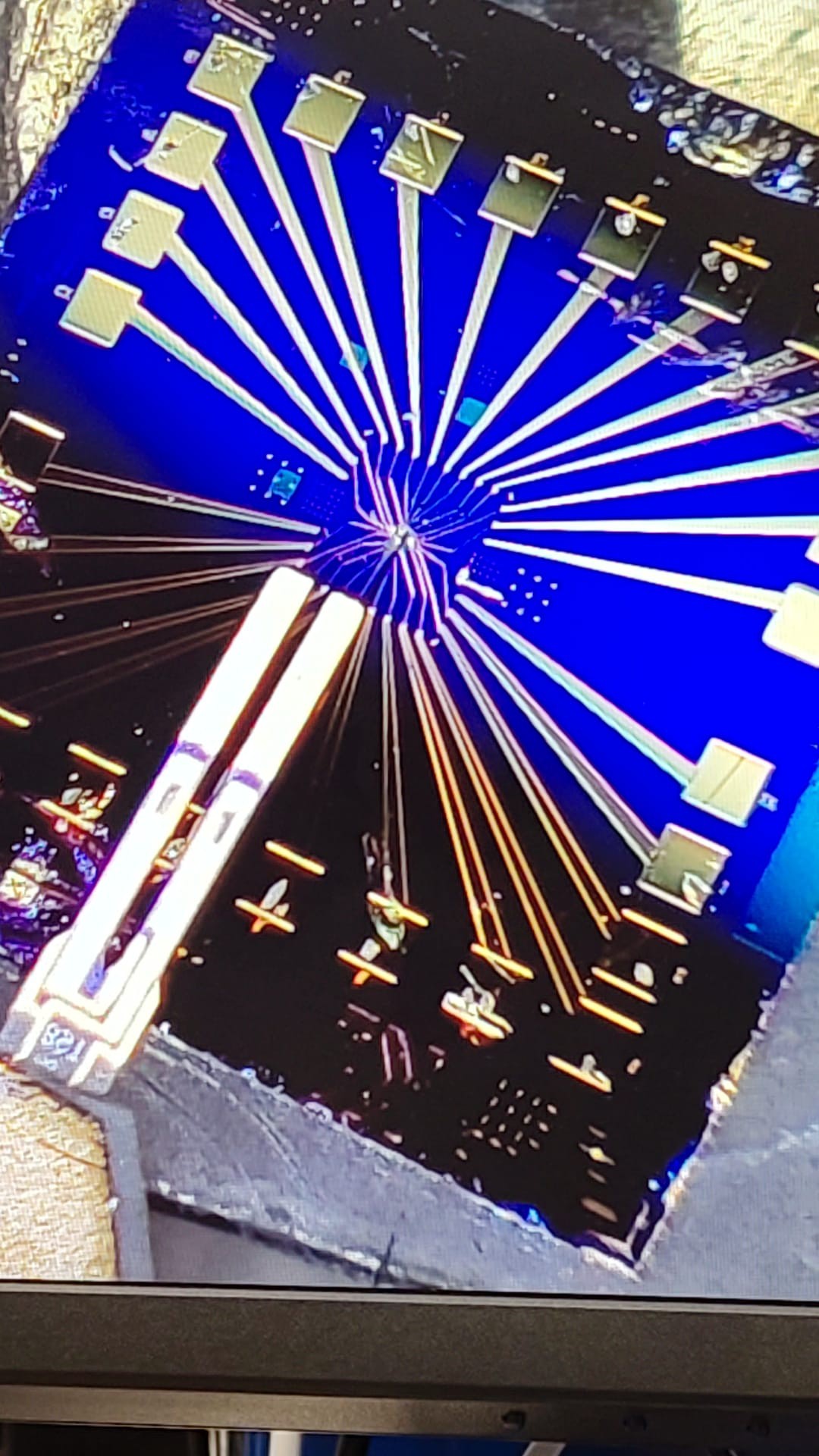
below is the setup the device is in the middle of the wires
![]()
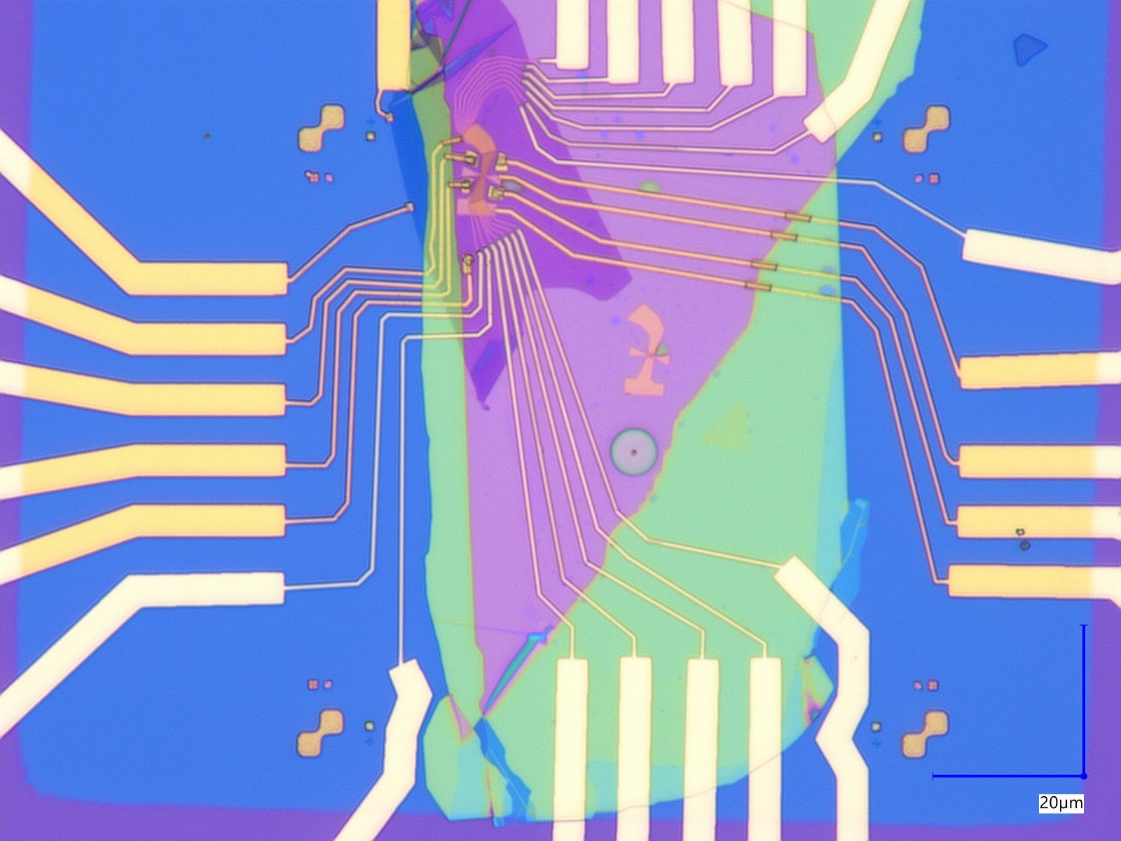
Here is the optical microscope image
![]()
I believe this image is on one of the edges of the flake, as I didn't have a great microscope to check where I was and the tip is moved with a hand micrometer stage. With only 15x15um scanning range and the images taking a while it's hard to hit the actual 10ish um device (I didn't have too much time that evening). However, it is still possible to see the 10nm high wires and the graphene should be quite thin as well.
![]() These are all half images because I was trying quite a few things out and I am limited by the bandwidth of my loaded Z piezo buzzer. This means I have to scan quite slowly and the images with high resolution can take quite a bit of time compared to a standard cantilever AFM that will take like 3 min. I actually compared my images to the system we have in the building costing upwards of 200k and mine are really not that bad especially if you don't mind waiting.
Conclusion:
-The system is currently working reasonably well
-The bandwidth on the z axis needs improving to run the PID faster in order to decrease scanning time
-The hysteresis of the stage is a working progress and will likely be solved with some initial hysteresis calibration before the scan using some rough displacement sensors like strain gauges on the stage to get the hysteresis curve and fit and then run the stage open loop (this should hopefully get it down to like 1% or so)
-Need a motorised rough positioning micrometer stage or stick slip piezo setup similar to Edwin's design https://hackaday.io/project/185518-hacking-any-linear-slidebearing-into-piezo-motor.
Basically the project is still a working progress but I think it's getting there and it's in a good state as it stands even just to play around as a hobbyist looking at cells butterfly wings etc, if anyone has any ideas for easy samples to prepare it would be great if you could drop a comment.
A working DIY atomic force microscope
The atomic force microscope for the masses
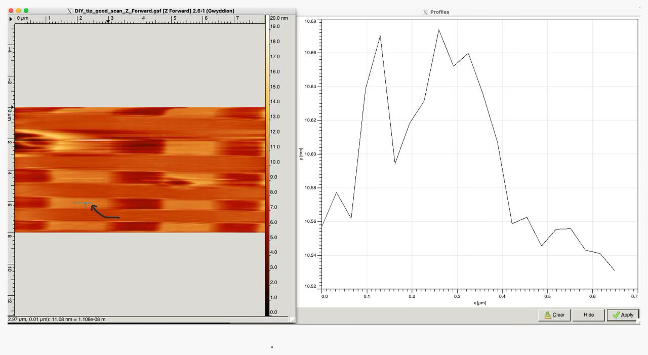 This seems to be reproducible across images. At some point I tried cleaning the AFM grid with some IPA in my lab which was very dirty and now the grid looks like this until I take it into the cleanroom and dip it into some piranha solution. But one can still see sub nm resolution. worth mentioning, this is with two different tuning fork tips one is the commercial one I got from my lab for free which is the one below and the one above is my DIY tip. My DIY tips actually behave much better with easier PID tuning since they are tapping mode rather than shear mode but when well tuned the shear mode one can also provide good images. On the image below I also changed the piezo preload on the stage and it's not quite as good as the previous that I will go back to so bear that in mind but this is just a rough resolution estimate exercise.
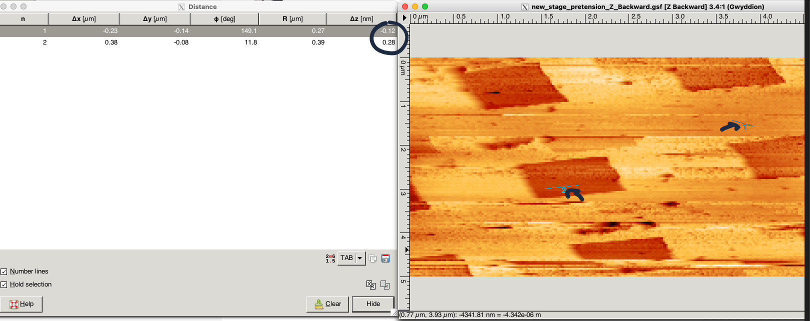 I noticed the current resolution is dependent on both electrical noise floor and PID settings but it's far more dependent on PID settings as the PID can be tuned well even with a noisy signal, and the topography scans can look clean despite the amplitude scans looking quite dirty. Electrical noise seems to be mostly dependent on the shielding of my transimpedance amplifier and cables leading to the tuning fork more than the stm32's ADC and I will at some point document these tests here. As I found out I am mostly limited by Jonhson noise of the feedback resistor and other random factors meaning there is no point in getting a better ADC than the STM32's 12bit ENOB one which already gets me subnm resolution and comes within the very cheap microcontroller instead of an expensive external one.
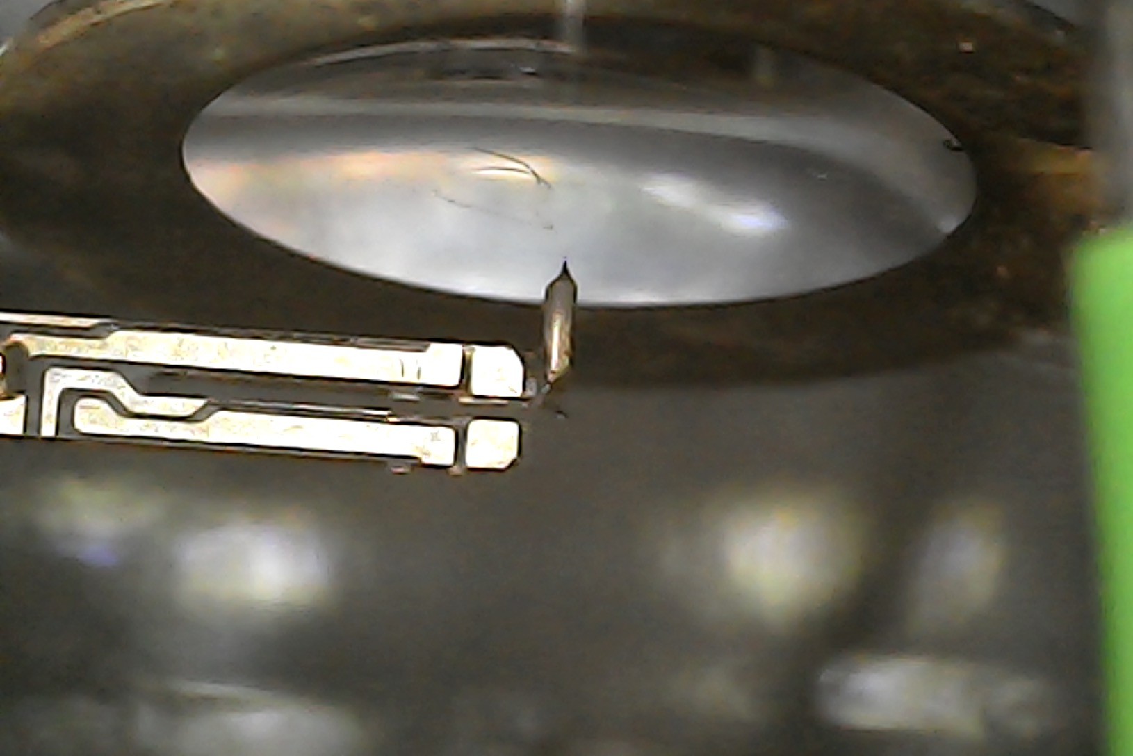

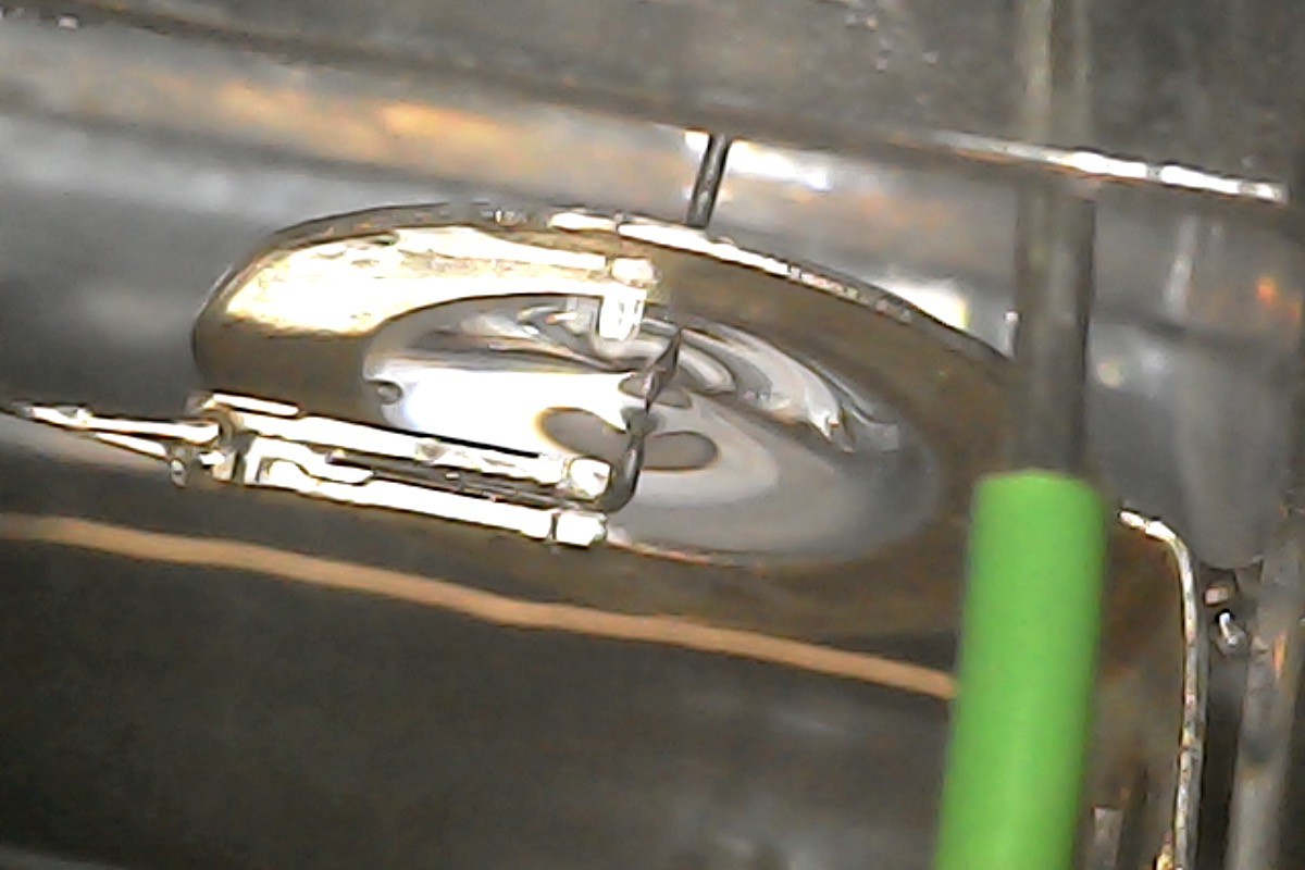 At this point you should have a tip that works, the full process with this nice little etching station takes about 20 min I don't really wait 24 hours like the mad city labs tutorial says to, I make them and scan right away and it works fine.
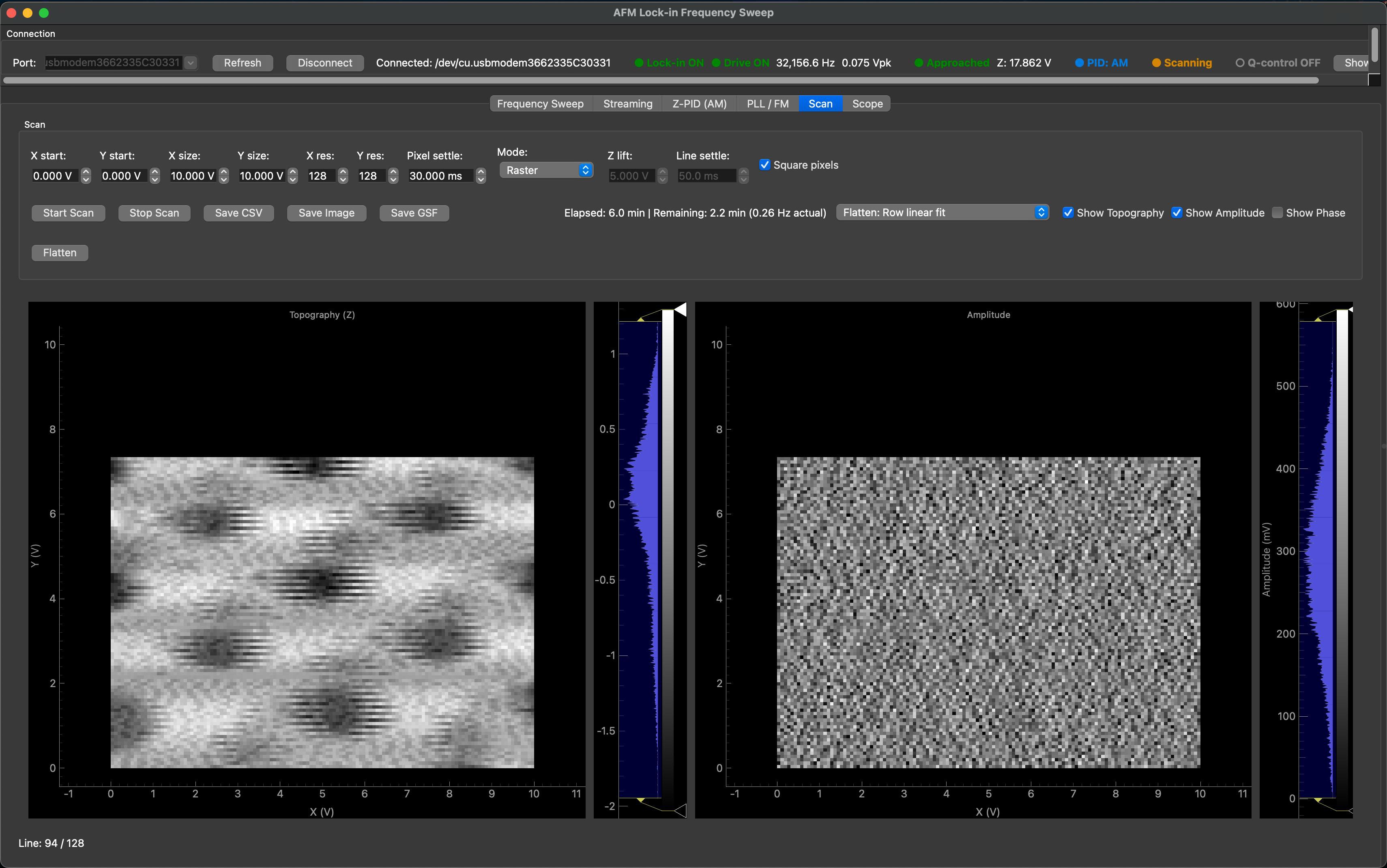
 Here is an example of the 20nm step with improved noise. The previous steps looked like this:
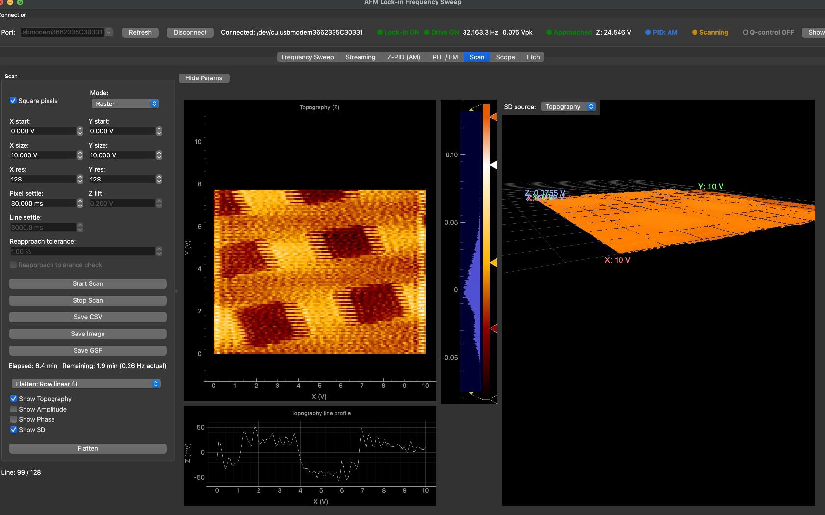 With the improved shielding on the tuning fork wires to the TIA the same 20nm step is much cleaner. I believe now I am limited by environmental vibrations due to my damping being a bike inner tube, to see atomic layers, I likely need and enclosure and the setup suspended by springs with eddy current damping from magnets similar to Dan Berard's STM. but I would say this is pretty good already for most applications like looking at cells or DNA.
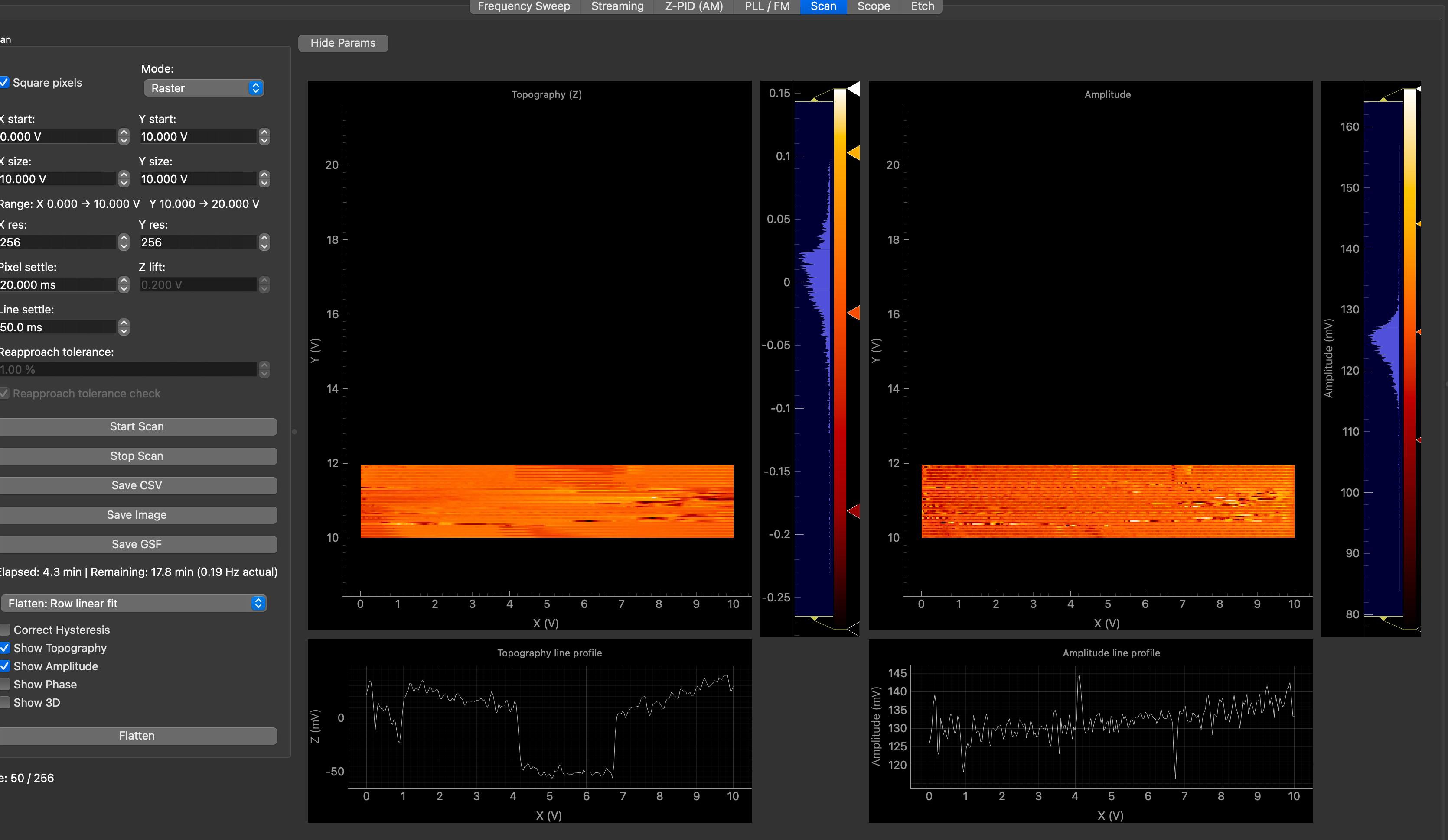 I also imaged the connections wires to a graphene device kindly given to me by a friend where you can see 10s of nm high wires, It's a little hard to see in the topography image without better processing in gwyddion but you can see the e-beam evaporated gold wires coming out from the graphene flake in the amplitude scan quite well.
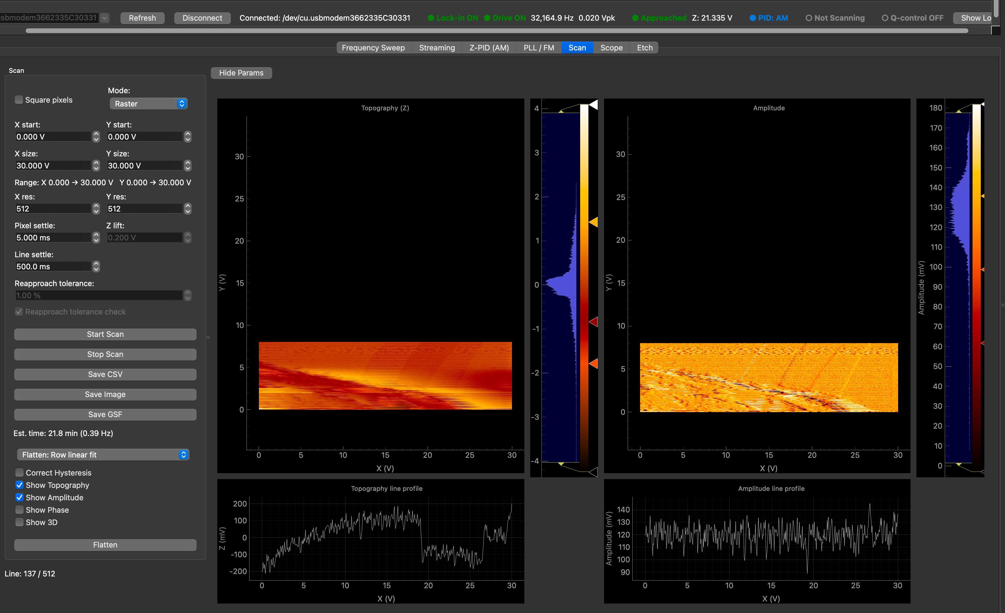 These are all half images because I was trying quite a few things out and I am limited by the bandwidth of my loaded Z piezo buzzer. This means I have to scan quite slowly and the images with high resolution can take quite a bit of time compared to a standard cantilever AFM that will take like 3 min. I actually compared my images to the system we have in the building costing upwards of 200k and mine are really not that bad especially if you don't mind waiting.