Close
0%
0%

Spartan-6 FPGA Retro System

A complete retro computer system on a single Spartan-6 FPGA. Integrates VGA (640x480), text & sprite engines, PS/2, UART, SD Card, and a cus

Similar projects worth following
0 followers
A complete retro computer system on a single Spartan-6 FPGA. Integrates VGA (640x480), text & sprite engines, PS/2, UART, SD Card, and a custom CPU interface with dual graphics buffers.

A custom FPGA system built on the Xilinx Spartan-6 XC6SLX9 chip. The project integrates multiple classic controllers and modules into a single chip, creating a platform similar to a retro computer. The system is written entirely in Verilog HDL and synthesized in Xilinx ISE 14.7.

It provides a complete graphics and I/O platform: VGA output with framebuffer, text and sprite engines, PS/2 keyboard, UART, SD card support, and a custom CPU interface for issuing commands.

ARCHITECTURE

The CPU communicates with the FPGA through a parallel bus with a 16-register memory map (ram[0]...ram[15]). The interface supports two synchronization methods:

- Interrupt-driven mode — the FPGA asserts the INT line when an event occurs (e.g. command finished, UART data received, PS/2 key pressed).
- Polling mode — the CPU periodically reads the status register ram[15] to check flags (busy, data ready, error).

Both methods can be used simultaneously — the CPU can enable only selected interrupt sources via the interrupt enable register, and poll the rest.

FEATURES

Graphics
- VGA Controller — generates standard 640x480@60Hz VGA signals (HSYNC, VSYNC, RGB) using a 25 MHz pixel clock.
- SRAM Framebuffer — external SRAM uses a 16-bit data interface. The framebuffer uses 8-bit RGB332 pixels, with the lower byte (LB) and upper byte (UB) available as separate graphics buffers. The active buffer can be switched by CPU command without stopping VGA display.
- Graphics Commands — CMD_DRAW_LINE uses Bresenham's algorithm to draw lines, with support for line thickness and dashed style. CMD_SET_BUF_LB and CMD_SET_BUF_UB select the lower or upper byte of the SRAM data interface as the active graphics buffer.
- Text Engine — 80x60 character mode with 8x8 pixel font. Supports cursor with adjustable height, color, and blinking.
- Sprite Engine — 8 independent sprites, each 16x16 pixels with 8-bit color. Supports per-sprite transparency (color 0), horizontal/vertical flipping, and enable/disable control.

Input / Output
- PS/2 Keyboard — full bidirectional PS/2 controller. Receives scan codes and decodes them to ASCII. Supports Caps Lock, Num Lock, and Scroll Lock with LED control. Handles extended keys.
- UART — universal asynchronous receiver/transmitter with 5 selectable baud rates: 9600, 19200, 38400, 57600, and 115200 bps.
- SD Card — SD card controller operating in SPI mode. Supports card initialization (CMD0, CMD8, CMD55, ACMD41, CMD58), block read (CMD17), and block write (CMD24).

CPU Interface
- Parallel Bus — 5-bit address, 8-bit data, with CE_n, OE_n, WE_n signals. A bidirectional buffer (ENABLE, DIR) controls the data flow direction.
- Command Interface — 16 memory-mapped registers (ram[0]...ram[15]). The CPU writes command parameters, then writes the command number to ram[0].
- Interrupt System — dedicated INT output line with 8 individually maskable sources: timer overflow, PS/2 data ready, UART RX/TX, command done, and RTS change.
- 8-bit Timer — configurable prescaler and reload value for periodic interrupts.
- Pseudo-Random Generators — 8-bit and 16-bit LFSR.
- Real-Time Clock — Unix timestamp counter (32-bit) with 1-second resolution.

TECHNICAL SPECIFICATION

FPGA chip: Xilinx Spartan-6 XC6SLX9
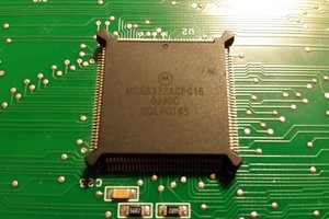
Package: TQFP-144
Language: Verilog HDL
IDE: Xilinx ISE 14.7
Main clock: 50 MHz
VGA pixel clock: 25 MHz
VGA resolution: 640x480 @ 60 Hz
Color depth: 8 bpp (RGB332)
Text mode: 80x60 characters
Sprite count: 8 sprites, 16x16 px each
Framebuffer: External SRAM, 640x480 pixels, 8 bpp per buffer
SRAM data interface: 16-bit
Graphics buffers: Lower byte (LB) and upper byte (UB)
CPU bus: Parallel, 5-bit address, 8-bit data
Interrupts: 8 sources, individually maskable

VERSION HISTORY

Version 1.1 (2026-10-10)
- Added CMD_DRAW_LINE, CMD_SET_BUF_LB, CMD_SET_BUF_UB
- Expanded SRAM data bus to 16 bits
- Added graphics buffer switching (LB/UB)
- Fixed bugs in thick_step and thick_begin

Version 1.0 (2026-10-06)
- First public release
- VGA, SRAM framebuffer, text engine, sprite engine
- PS/2, UART, SD card...
Read more »

FPGA_VGA.pdf

Complete schematic (PDF) — includes FPGA pin assignments, external SRAM connections, VGA output connector, PS/2 keyboard connector, UART interface, SD card slot, power supply section, JTAG programming header, CPU parallel bus connector, and interrupt line (INT).

Adobe Portable Document Format - 88.71 kB - 10/12/2026 at 22:52

Preview

atmega_demo-v1.1.zip

ATMega demo code (v1.1) — demonstrates the buffer switching commands (CMD_SET_BUF_LB, CMD_SET_BUF_UB) and basic graphics drawing on the FPGA platform. Written in C for ATMega microcontrollers. Contains: - main.c — main demo loop - vga.c / vga.h — VGA command interface - uart.c / uart.h — UART communication - Makefile — build script

x-zip-compressed - 29.21 kB - 10/12/2026 at 22:51

Download

FPGA-Spartan6-XC6SLX9-v1.1.zip

Verilog HDL source code for the FPGA Spartan-6 XC6SLX9 project (v1.1). Contains: - main.v — top-level module - vga_timing.v — VGA 640x480@60Hz generator - sram_ctrl.v — SRAM framebuffer controller - cpu_ram.v — CPU command interface - text_engine.v — text mode 80x60 - sprite_engine.v — sprite engine (8x 16x16) - ps2_keyboard.v / ps2_decoder.v — PS/2 controller - uart.v — UART controller - sd_spi.v — SD card SPI controller - rom_font.v — 8x8 font ROM - config.vh / fpga_regs.vh — configuration headers

x-zip-compressed - 49.35 kB - 10/12/2026 at 22:49

Download

  • ATMega demo code released

    rick1961pl • 3 hours ago • 0 comments

    The atmega_demo-v1.1.zip archive contains CPU-side demo code for ATMega microcontrollers. It demonstrates how to use the buffer switching commands and basic graphics drawing.

    Download it from the Files section.

  • Bresenham line drawing

    rick1961pl • 3 hours ago • 0 comments

    CMD_DRAW_LINE (23) implements Bresenham's algorithm with support for line thickness and dashed style. The command takes 5 parameters: start X/Y, end X/Y, color, thickness, and dash style.

    Fixed two bugs:
    - thick_step: stray pixels when drawing thick lines — used $unsigned casting instead of truncating the sign bits.
    - thick_begin: added clearing of wr_req before starting a new thickness block.

  • Buffer switching with VBlank synchronization

    rick1961pl • 3 hours ago • 0 comments

    Version 1.1 added graphics buffer switching (CMD_SET_BUF_LB / CMD_SET_BUF_UB). The switching is synchronized with VBlank to avoid tearing — the buffer swap happens only during the vertical blanking interval (v_cnt >= 480).

    Implementation:
    - Added vblank output to vga_timing.v
    - Added ST_WAIT_VBLANK state to cpu_ram.v
    - Buffer swap is triggered by rising edge of vblank

    This ensures the VGA display never shows a partially-drawn frame.

  • Project Introduction

    rick1961pl • 3 hours ago • 0 comments

    Project Introduction

    This is a custom FPGA system built on the Xilinx Spartan-6 XC6SLX9 chip. It integrates multiple classic controllers into a single chip: VGA (640x480), text engine, sprite engine, PS/2 keyboard, UART, SD card, and a custom CPU interface.

    The project is written in Verilog HDL and synthesized in Xilinx ISE 14.7.

    Version 1.0 was released on 2026-10-06.
    Version 1.1 was released on 2026-10-10 with new graphics commands and 16-bit SRAM buffer switching.

View all 4 project logs

  • 1
    The system is controlled by a custom CPU through a simple command interface.
    Command Execution Flow:
    1. Write parameters to registers ram[1]...ram[9].
    2. Write command number to ram[0] — this starts execution.
    3. FPGA executes the command — the busy flag in ram[15] is set.
    4. Wait for completion — either poll ram[15] bit 0, or wait for the INT line.
    5. Read result from ram[15] (status) or specific registers.
    
    Interrupt Handling:
    1. Enable interrupts — write mask to ram[18].
    2. Wait for INT — the FPGA asserts the INT line when an enabled event occurs.
    3. Read flags — read ram[16] to see which interrupt fired.
    4. Handle event — perform the required action.
    5. Clear flags — write 1 to the corresponding bits in ram[17].
    
    Full details: https://github.com/rick1961pl-ops/fpga-spartan6-code1

View all instructions

Enjoy this project?

Share

Discussions

Similar Projects

Does this project spark your interest?

Become a member to follow this project and never miss any updates