Tom Anderson
-
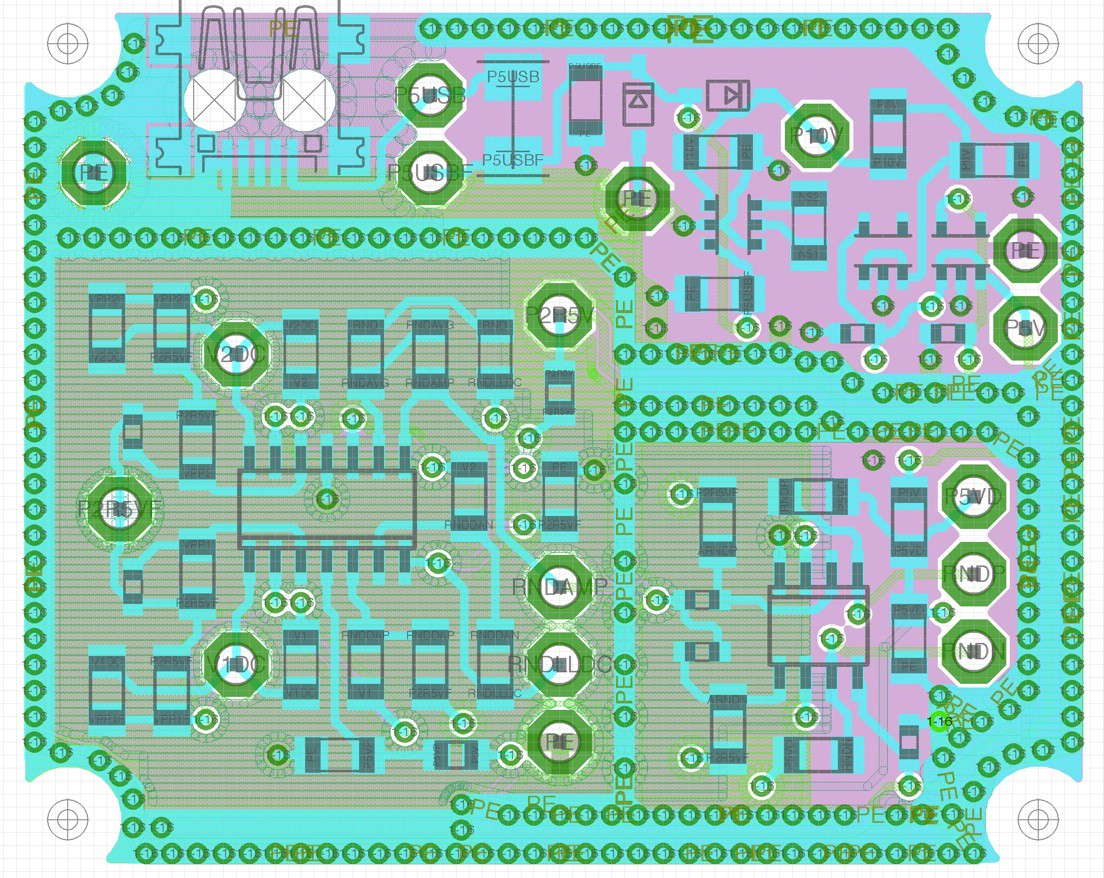
PC board layout copper design finished
04/29/2017 at 23:31 • 0 comments
I have uploaded the latest EAGLE file.
Learning EAGLE has been an adventure. There was one crash that kept happening and it really bothered me. I was able to get help from EAGLE support with recovery. To me, the way the backup files work was not intuitive. For some reason I don't understand, I have stopped doing whatever was causing the crashes, for the most part.
I also tried the BOM upload feature for the Findchips interface, but it did not like my Digi-Key part numbers. I was able to chat with the Findchips developers and they are interested in adding this feature. I like distributor part numbers because they solve various issues:
Here is what I told them:
"I have multiple manufacturer part numbers for each part, because I've already thought about multiple sourcing and have an Approved Manufacturer List (AML)
I like Digi-Key part numbers, because they are truly unique (MPNs are not unique! The same MPN can be used by different manufacturers for totally different products.) Manufacturer Names or IDs are not controlled keywords, unless you get into using Dunn's numbers (which I am not).
I like Digi-Key (or other distributor) part numbers because they distinguish cut tape from a whole reel of parts, or the different carriers for chips, etc.
MPNs sometimes vary with packaging, also, for example how many parts are on the reel, the width of the reel, etc.
Ideally, I would like a BOM spreadsheet .xlsx template that supports an AML and Digi-Key part numbers."
-
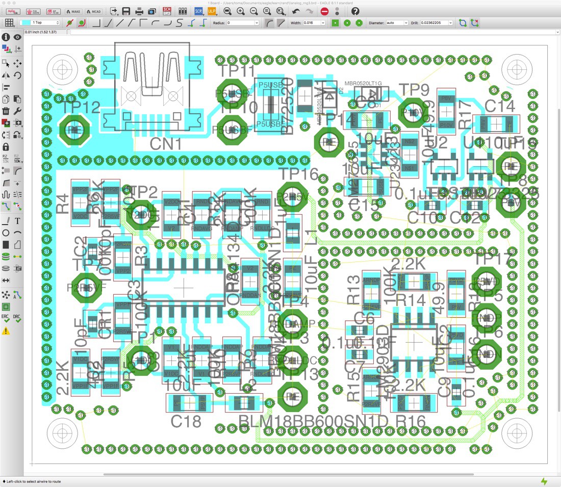
RNG Layout in progress: using EAGLE 8.1.1
04/23/2017 at 09:28 • 0 commentsI have been learning EAGLE layout. My review so far is "Good, not bad. Could be better."
I like the interactive routing, and the MOVE command works well for moving existing routing. Not all tools are good at this. I need to learn more to do a real comparison. After using PCB layout for about 12 hours, I think I am better at it than I was after using gEDA/PCB for 12 hours. I am much better than I was with much more expensive CAD tools after 12 hours. I haven't tried KiCAD for that long, so I have no comparison for it.
There are some things that bother me about it: The polygons are painted, and not very well. This means that sharp-cornered polygons don't seem to be possible. After a while of using gEDA/PDB, I got to the point where I could make it do anything that I wanted. With EAGLE, I have to make the usual tradeoff: I can't draw exactly what I want, but what I can draw is more productive.
There has been one crash, but I lost very little work by manually renaming an auto-saved file. It did not offer to restore this file for me. The program briefly flashed an error message about some missing object as it went down during an UNDO. After launching it again, it didn't offer me an auto-saved file, and it had been 30 minutes since my last SAVE. Weird. I found the tip that the autosave files exist from Google search results. Google results are one of the best parts about EAGLE. There is a lot written about it online. EAGLE has more good advice online than the Open Source tools I have used. It also has much more online than the 100X and 1000X more expensive tools. If you are using the Guess-Google-Guess-Google... learning cycle, it works fine.
There are some delightful things about EAGLE layout. One is the icons. The downside of my 4k monitor is that many applications have tiny icons and no way to make them larger. Some applications let you scale the Icons. The EAGLE 2X icons have high resolution, and they are just the right size on my 4k display. They are crisp! This is a true retina application. Nice! This is my first PC layout design with a 4k monitor. There is no way I am going back, because 4k layout is amazing. Applications without scaling capability have fallen behind where they need to be.
In the example screenshot, there is a lot of label clutter because I have the component values turned on. It looks better with just reference designators and net names. The net names help. For this type of layout, I am not just making connections. Layout is an important part of the design, and I have to understand exactly what I am hooking up, and how. There is cross-highlighting to the schematic to help with this. Also, I have named all the nets, and now I am getting the payoff for this extra work.
The proof of the CAD tool is in the Gerber output. I won't really know what I have until I look at the design in an independent tool.
-
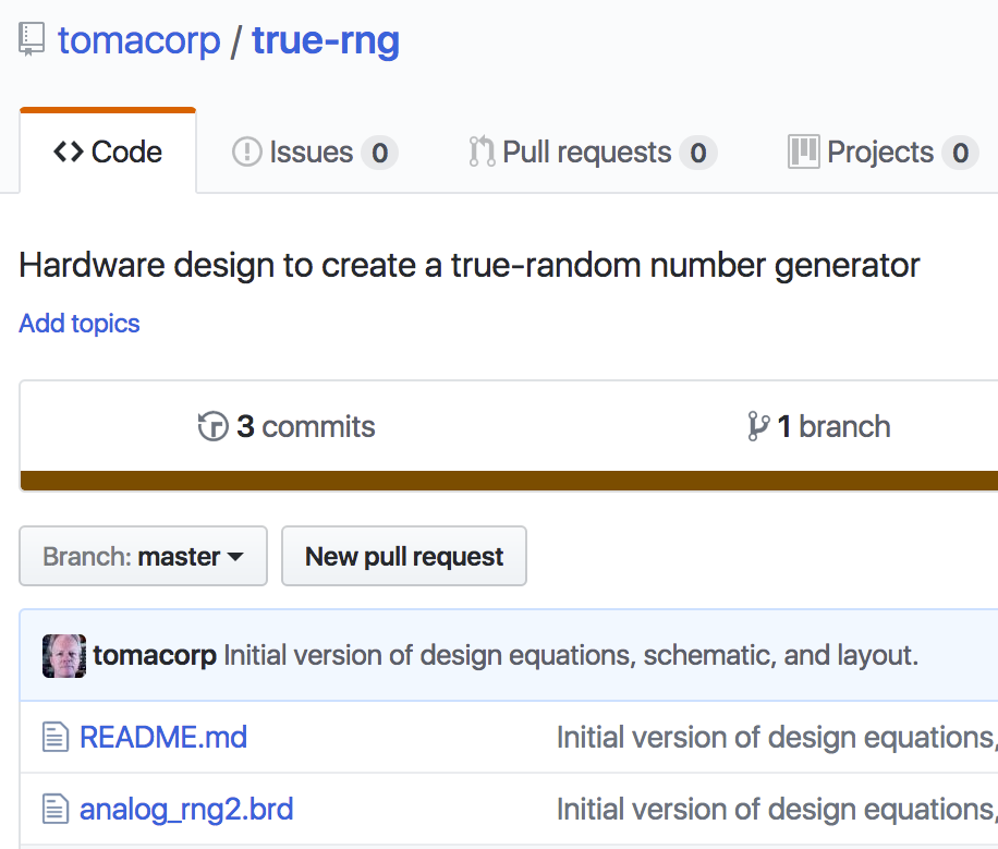
Work-in-progress design uploaded to Github
04/20/2017 at 07:17 • 0 commentsThe design spreadsheet, schematic, and layout are now at https://github.com/tomacorp/true-rng . The README has been updated with the license, which is MIT.
If anyone is interested in the analog design technique that I am using, please let me know. I think there is a lot written about how to analyze circuits, but not so much about how to design them. It would be good to hear what people want to read about. I could take many different directions with the writing.
The schematic is not too bad but the layout is really rough. I have the first cut at a placement done, and a little bit of routing. I can see that I should rip up all the routing, refine the placement, and route again.
One of the things that engineers often wonder is, "When is the design done?"
When I build a board, my intention is to make it as good as I know how. I have ordered production quantity boards on a new PC board layout first cut, and shipped them with no modifications needed. The reason for this is that when ordering boards, it is not that much more expensive to get more, as long as you don't mind waiting a few weeks for the boards. It is just too tempting to have more.
For this project, I don't intend to sell anything, although I might if there is sufficient interested. However, I have discovered that I enjoy improving designs until I can find any ways to make them better. That is when I know the design is finished: I can't find anything to improve.
This is my first EAGLE board. In my experience, the first board in a new CAD tool is disappointing. How will EAGLE work out? Checking will help. I should look at every part footprint and pinout. I intend to simulate the design. To do this, I will hook up a Spice simulator and bring in my simulation models. This design is about random noise, and Spice can calculate noise spectral density versus frequency. I can integrate the noise data across frequency to find the RMS value of the noise. There is also more to simulate such as a switched-capacitor power supply, voltage regulators, and filtering.
The design spreadsheet is an xlsx file. I wish there was a great spreadsheet application for electronic engineering! I used to use an open source spreadsheet called sc written by James Gosling. I contributed to sc back in the day. While writing this, I checked and found sc on github. If you are into code archeology, try it out!
-
Designing a PC Board for the RNG
04/19/2017 at 17:50 • 0 commentsEnter constraints, derive component values, choose components, draw schematic, draw layout. Welcome to analog land!
The constraints are in Excel. To really check to make sure that everything will work, I can use a simulator. More time in the simulator increases the odds of first-pass success.
The challenge with this design is to make a random noise source where the noise comes from a well-known, testable source. Other components are not allowed to make a significant contribution to the noise. The intended noise source is a pair of 100k resistors. I think of the thermal noise from these resistors as the 'signal', which I need to process in a low-noise way. This is similar to a sensor project, in that I need to take a low-level signal and amplify it to a useful level. Since thermal noise is a low-voltage phenomena, the signal level from it is low. How low? Noise is interesting that way - the more bandwidth there is to measure it, the more noise there will be. Today's version of the design has 13.3kHz of bandwidth, and for two 100k resistors, the noise level comes out to 20.8uV RMS.
I call the resistors being measured the 'physics package' and the noise coming from them the 'signal'. The noise from the circuit that is not from the resistors is still called 'noise'.
To get low noise, I am using the OPA4134 opamp. The resistors are thin-film 0.1% 25ppm/degC. The design technique is the same that I use for designing test equipment. The board will be four layers, with a solid ground plane and a split ground/2.5V plane, and two routing layers. This, and far more power filtering than you might think would be strictly necessary, are important for building accurate circuits with low-level signals.
The network with L1 and C17 is designed using the technique from my blog post "Power Supply Filter Design for Printed Circuit Boards". The damping comes from the series resistance in the bead L1. When I run a simulation of the board, I should be able to post performance results for the power supply bypassing as well as the noise.
This is my first EAGLE schematic and there is still some cleanup to do. I also need to run a simulation, but I haven't chosen my approach for how to do that. In making the EAGLE schematic, I made a local library in the design that has the parts that I am using. I created the library by cutting, pasting, and editing the XML library file in Sublime Text. For me, this is easier than a GUI. Understanding the data format is the main way that I learn CAD tools. In my mental model, a GUI is a tool that makes it easier to create a design database. If I can't easily see the design database, the tool is much harder to learn. EAGLE is delightful this way! The symbol, schematic, and layout files are human readable.
This schematic is good enough for a first-pass at layout. There are plenty of library problems that I see in layout, and I don't quite have the UI tamed yet, so it looks like this:
My plan is to rip up the routing, adjust the placement, and route again. There is a 'long pole' starting at the resistor R5 sticking out the bottom row. This is not so hard to fix, and I need to move V1 and D1 close to the top anyway. There is plenty of free space. I am using wide traces to make the board easy to modify without damage. When traces are too wide, they are hard to cut. When they are too narrow, they become too fragile. The optimum width for rework is in the .012" to .025" range. Wider traces in this range are easier solder wires to. There are big test points on all the important nodes, except where there are space issues. There are a lot of test points on ground! Space around the edge of the board, and plenty of mounting holes make it much more fun when it is time to work on the board.
The resistor noise sources are R1 and R3. The layout is symmetrical for these two parts, which creates a string of devices starting with R5. There is a traffic jam around C15. There is plenty of room to solve these problems, but taking advantage of it means that the existing routing has to go! This is no problem, though. I am getting better at manual routing anyway.
-
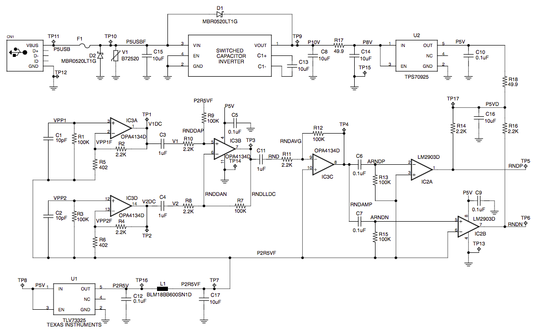
The True-Random Number Generator schematic
04/10/2017 at 20:04 • 0 commentsI have been learning EAGLE while drawing the schematic. I just bought a subscription using a 50% discount from being a (free) circuit.io registered user. $50 a year. Not bad, worth a try.
Here is what I have been working on from the point of view of the analog design. The reference designators correspond to the schematic in the project description.
In my next iteration (coming soon!) the values for R16 and R17 are 100k. The noise from R16 and R17 is amplified by U1A and U1D. These two amplified signals are then subtracted from each other by U1C. This subtraction operation cancels out any external interference that might be picked up by R16 and R17. After subtraction, there is another gain stage, and then a comparator to make a bitstream. For more detail, the patent explains every component, if I recall correctly.
The op amps U1A and U1D need to be low-noise in order to prevent the op amp noise from overwhelming the resistor noise. I am using the OPA4134, which I have used before. The resistors are 0.1% thin film 0805 25ppm/degC. Good resistors are important for good cancellation. They also have nearly the same noise as an ideal resistor. This is unlike thick-film resistors, which have more noise than that.
This is an instrument-grade design that is not optimized for cost. The idea is to have a well-controlled circuit that is easy to measure. The goal is to be easy to show that the source of numbers is truly random thermal noise from the resistors. If I were to make a lot of these, perhaps there will be a reduced-cost version.
I have a spreadsheet with all the component value calculations and signal levels, and I will post something about that after I clean it up. I might turn it into a Python program or something.
The changes I am working on will enable the circuit to run off of a USB supply. At some point I will provide a USB interface to send the output to a computer. I could do this with an Arduino, but I might use something else.
The power supply design is coming out a little weird, because it turns out that people don't seem to use negative supplies very much these days. Negative-voltage low-dropout voltage regulators are expensive and uncommon. I am changing the design to use all positive supplies. Analog circuits without negative supplies are much harder to understand. No wonder EEs have trouble learning analog these days! I think I have figured out a way to draw the schematic so that it looks as simple as a bipolar design, but uses all positive supplies.
This has been a good way to learn EAGLE, because I am spending a lot of time editing the schematic and learning how things work. I am quite particular about both schematics and layout. They are finished when I can't find anything more that can be done to improve them, either electrically or otherwise. The main problem with EAGLE is that I think the libraries are ugly. The file format is beautiful XML, though, so I might port a better-looking library to it. Would that be procrastination? I you don't hear from me for a while, that would be 'yes!'
True-Random Number Generator
Modern security and cryptography call for a source of true-random numbers. This design creates them from thermal noise in a resistor.