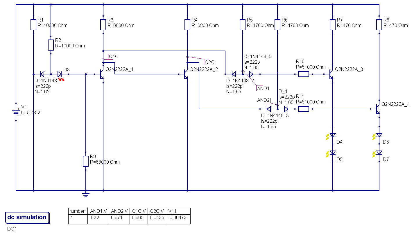
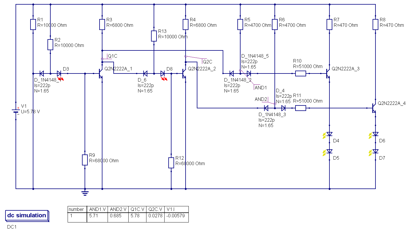
The humble diode AND was not to blame after all, it was prior wiring that was faulty.
Here are simplified schematics with voltages:
1) original wiring:
 collector of Q1 was wired directly to base of Q2, to achieve second inversion, thus making buffer; simultaneously from the same collector was the tap to the AND gate of decoder, as inverted input. Failed. the solution was to make this into two full-fledged invertors, and after this modification all started to work as it was intended to.
2) corrected wiring:

 Pavel
Pavel
Discussions
Become a Hackaday.io Member
Create an account to leave a comment. Already have an account? Log In.