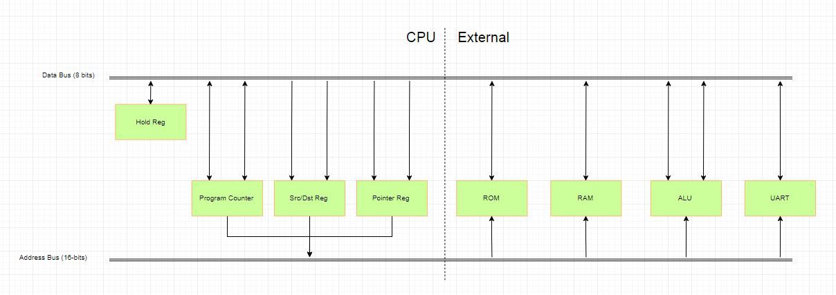
I redesigned the top-level block diagram so that it illustrates the new datapath better. It's much simpler than the previous one, but it doesn't have the TTL chips called out. This makes it simpler to understand the operation of the different functions. I'd like to be able to animate it and make a gif out of it so I can show what happens in the 6 clock cycles per instruction, but draw.io doesn't support it. I would like to have a better flowgraph program, but I do like open web-based tools.

Breaking down the system like this makes it much easier to understand its simplicity. The CPU only really controls which of the three 16-bit registers control the address bus, and then decodes the address bus for reading/writing of its own 16-bit registers to/from the data bus. It starts to look a lot like a normal 1970s CPU interface (like a 6502 for example). Perhaps I could make two different PCBs - one for the CPU and one for the external peripherals - just to show what parts the CPU could be if put into an ASIC.
Discussions
Become a Hackaday.io Member
Create an account to leave a comment. Already have an account? Log In.