-
PCBs shipped!
11/16/2017 at 21:03 • 0 commentsPCBs are shipping from EasyEDA and will arrive probably Monday. I have also received all components. I have also updated my FPGA design to match the PCB, so I should be able to run the same software on both platforms. This will hopefully help me to debug any issues with the PCB. I have my assembly procedure listed on the project details page, and I plan to test as I go to make sure each part works as expected before I build the next part.
I also have my EEPROM programmer code all working. So I can generate an Intel HEX file to download to the EEPROMs for each of my three EEPROMs in the design. ALL SET TO BUILD!
-
Schematic uploaded
11/08/2017 at 13:08 • 0 commentsI forgot to upload the schematic for the PCB, but it's on here now. It's an 8-page PDF to make it easy to read. I could upload the design files if anyone is interested. I also updated the memory map spreadsheet.
-
PCB ordered
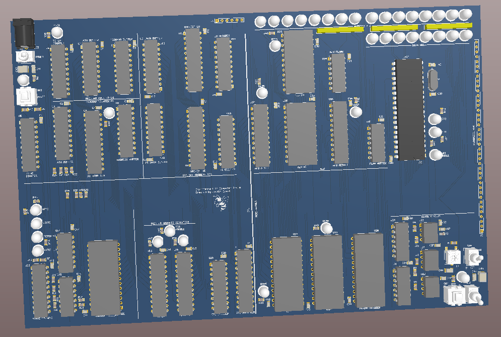
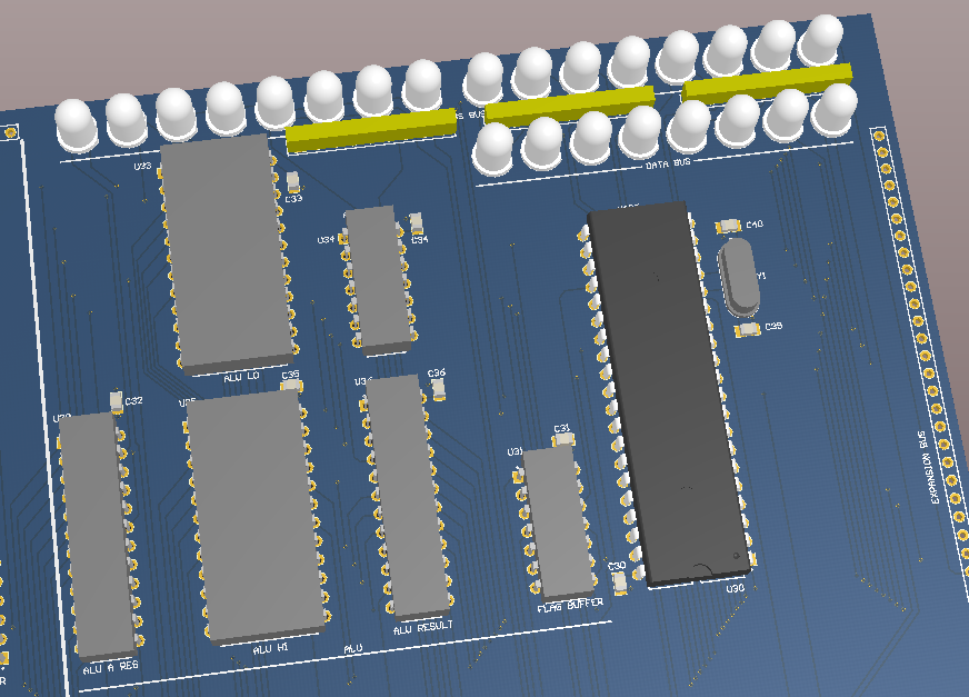
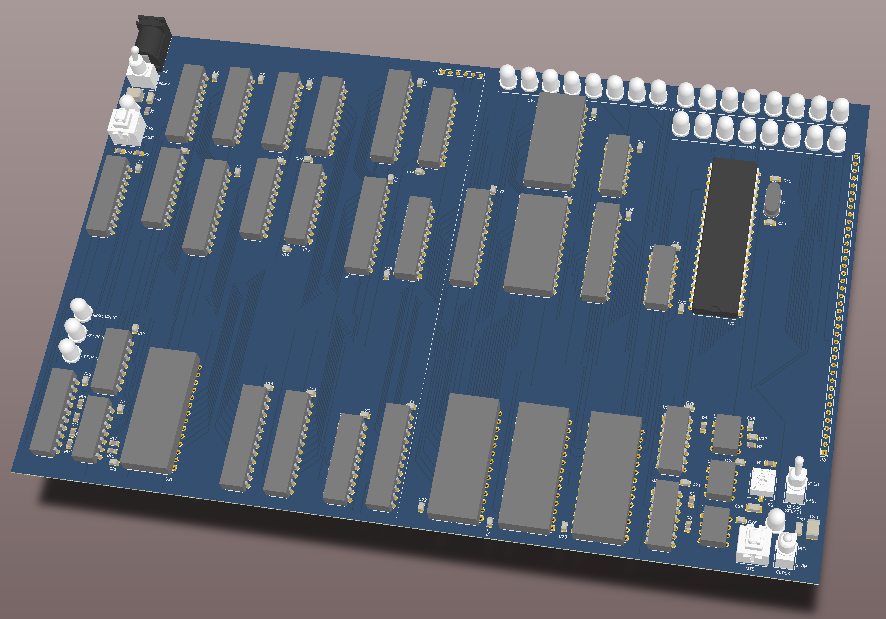
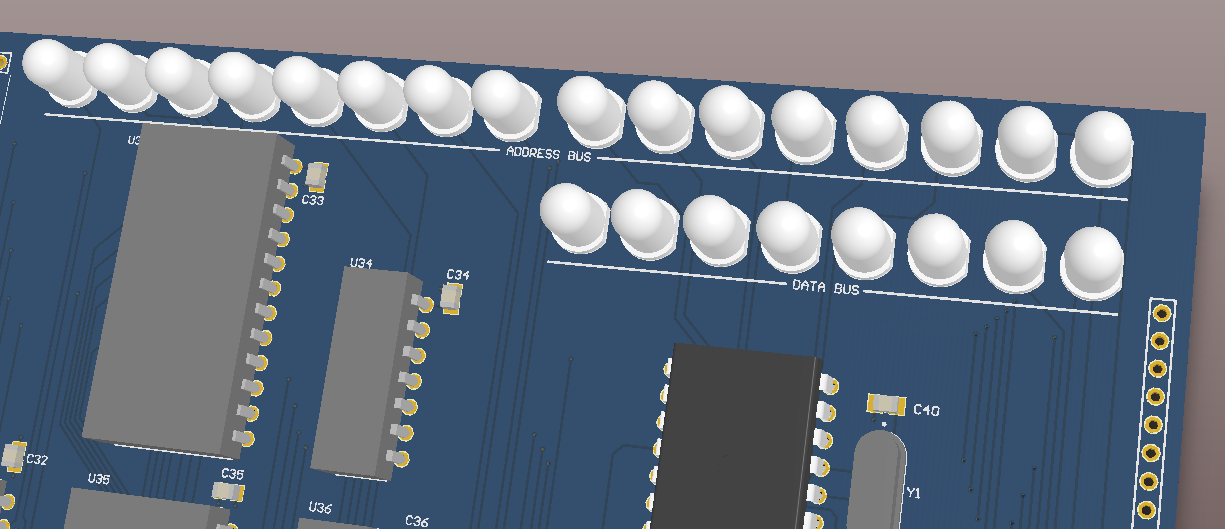
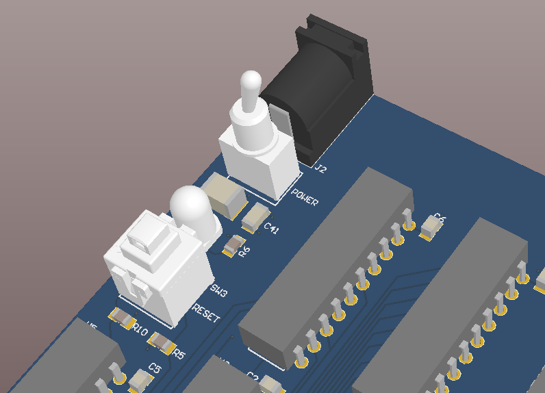
11/07/2017 at 19:13 • 0 commentsI finally have ordered the PCB. I've dragged my feet long enough, but they are paid for. Probably be 2-3 weeks. $60 plus $30 for shipping. I added a bunch of LED indicators for when each module is active. So when I step through the program I can see which chip is enabled. I had quite a bit of board space to use up. Hopefully I don't have too many mistakes (there's gotta be at least one in there). Now I'll have actual hardware to show off (besides an FPGA).
-
Do it right
11/06/2017 at 13:51 • 0 commentsI put some time into seeing if I could get away with not putting current-limiting resistors on my LEDs, and I realized I could not. My hope is I will get everything right with this board the first time, so I need to play it safe. It makes my design look not quite as good, but that's ok. I originally was going to use some surface mount resistors on the bottom side of the board to keep everything looking clean, but that's a lot of annoying soldering. So I switched to a few resistor arrays.
They block some of the silkscreen, but it's not too bad. I'll be looking down on it from directly overhead, and I'll know what it says. I also labelled each important TTL chip just to make it look a little better and it may help with debugging. I'm still considering putting more LEDs on here - maybe one for each chip when it's enabled.
My inspiration for a good-looking board is the transistor-level 6502 project: https://monster6502.com/
Mine will not be as good as this one, but it shows how much pleasant aesthetics can do.
-
Control simulation
10/30/2017 at 12:58 • 0 commentsI am never comfortable sending out a PCB without simulating first. I decided I had to simulate a few components which I had not. The control chip was one and it's a good thing I did. I found I had a combinational loop that oscillated. Spent a while, but got that fixed without adding more chips.
I also noticed in Ben Eater's videos that he drives a full bank of LEDs without current limiting resistors. I figured I'd just do it. And then the good engineer in me decided I need to double check it. TTL does have an internal pull-up resistor, so it's possible to do it. I measured the draw is 32mA and the datasheet maximum is 24mA. I think I should probably test to failure - it might be at room temperature it can handle more. Or I just put resistors on all 30+ LEDs which takes a lot more board space.
I also discovered some clock glitches while testing. My clock looks like it bounces on the falling edge, and I only caught it when stepping my shift register one clock at a time - it moved twice for every push. I still have the old wired-OR logic hooked up, so I need to put the TTL OR in place to see if that's the problem. More work before ordering PCB...
-
Blinkenlights!
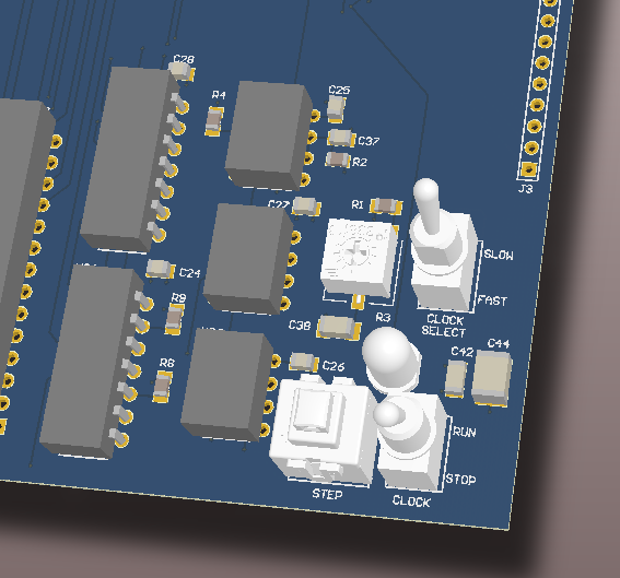
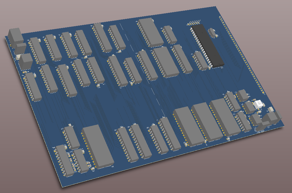
10/17/2017 at 16:31 • 0 commentsI've added some LEDs so I can easily check the status of my board. Now I can stop the clock, and step through the code while checking the data and address bus. And I have a few more for the control logic state machine since it takes 6 clock cycles to execute one instruction. I've also updated my 3D models to make it look a little nicer.
Other than more silkscreen to make it pretty, I'm not sure what else is needed. I'm still wondering if I should check some of these individual chips to verify they actually work like I'm expecting them. Sometimes these old datasheets are not verbose in describing the operation of the chips.
-
PCB Layout first pass done
10/13/2017 at 17:06 • 0 commentsThis board is a real bastard to layout. I can only imagine how much it would have taken if I did it on a solderless breadboard. Give me an FPGA any day.
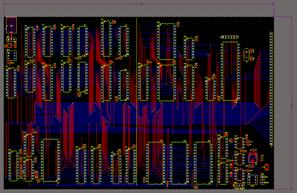
It's far from done, but everything is routed. I still would like to add some LEDs just for some blinkenlights and debug. And I need to add some silkscreen lettering to make it look really nice. But these dimensions are 243x155mm. EasyEDA says that's just under $60 plus shipping. The real question is: what mistakes are lurking in there?
-
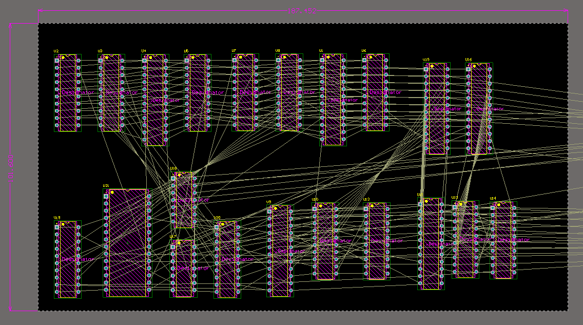
TTL schematic "finished"
10/06/2017 at 18:14 • 0 commentsI have everything on the schematic now that I think I will need for the TTL PCB. It only takes 8 pages and 36 TTL chips. Creating a PCB from the schematic shows me I have quite a lot of work ahead with routing the 16-bit memory bus and 8-bit data bus along with the clock and control signals. I will definitely need to go to at least a 4-layer board. Hopefully not more or things will get expensive. I figure I can stick to the simple rules of top layer traces run vertical and bottom layer traces run horizontal. And then lots of vias. I figure I will run the traces through the center of the board horizontally. And then pull them off up and down to the chips.
I'll probably also add some debug features later - maybe some LEDs on the busses to make everything look good. And I still need to add the breakout header for the bus. So it's not 100% done, but the essential components are on there. I will upload a preliminary schematic to the project as a snapshot of where I am.
-
TTL CPU schematic done
09/29/2017 at 14:53 • 0 commentsI've completed the schematic for the CPU portion of the design. It's a pretty big design - I'll post it here shortly. There's 21 chips just for the CPU. And just placing them on a PCB, it's about half the size of a standard piece of paper, but routing might make this bigger. I have a 16-bit address bus and an 8-bit data bus to route everywhere, so I will almost certainly have to do a 4-layer board. Estimating the cost of this - from EasyEDA this size of a 4-layer board is about $46+$8 shipping for 5.
Ok, I just checked if I double the size of the board (for the peripherals, clock, power) the price goes to $59+$8. So I may just put everything on a single board. It would cost a lot more to make two boards of the same size of a single large board. I'll still have an expansion bus for debugging and possible future projects (video out maybe?) I'll just have to make sure I get it right the first time. But then, it's only $59+$8 to rev it, right?
-
TTL back on the menu
09/22/2017 at 20:00 • 0 commentsNow that I've accomplished a milestone for the software (the BM9 benchmarking), I'm thinking I should swing back to developing the TTL version of the system. I'm pretty happy with the architecture. So I've been going back and doing the implementation in TTL. Eventually I'll make a PCB with it, but I might prototype it on a breadboard first.
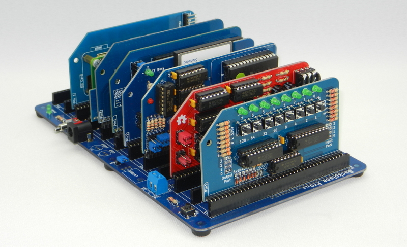
I'd like to split the project into two separate boards: an S100-inspired backplane with the CPU in one slot, and the peripherals in another slot. Here's an example I found on Google search for illustration:
![]()
Maybe I would have a separate clock board in another slot, but I may integrate that with the CPU. Maybe I would have a debug board which shows the data/address bus with LEDs. Of course having a big backplane would be expensive, so I'll have to see how large these boards need to be. And if I have all my boards stacked up, then they don't show off all their components as well. Looks go a long way. Perhaps I'll just split it into two just to illustrate how one board is the CPU, and the other side is flexible with ROM/RAM/UART, etc. Then I can lay them side-by-side and still be able to show off all the chips.
But schematic comes first, and I'm only maybe 1/3 of the way there.
image source: http://rc2014.co.uk/
One-instruction TTL Computer
A breadboard-able computer which uses only a single instruction - MOVE