Chris
Chris-
mk2 PCBS and Failure
01/11/2018 at 05:39 • 0 commentsAlright! So it's been a while since the last update. College Happened.
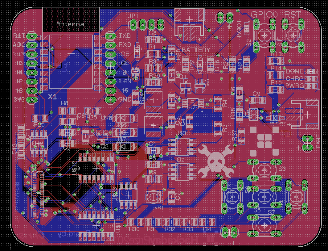
Since the last update I made a new pcb which is smaller, better, faster, stronger, etc. I used the ESP32 this time and I have to say that it was nice to get rid of those shift registers. In this version I also switched to 805 components to save on size.
I also moved the d-pad of buttons onto a separate pcb which really helped to bring down the costs as well.
All together the various design changes I made brought the costs of each pcb from 15 dollars to 5 dollars.
Honestly though it doesn't really matter because it still doesn't work :)
Enjoy some pictures and then read on to find out more.
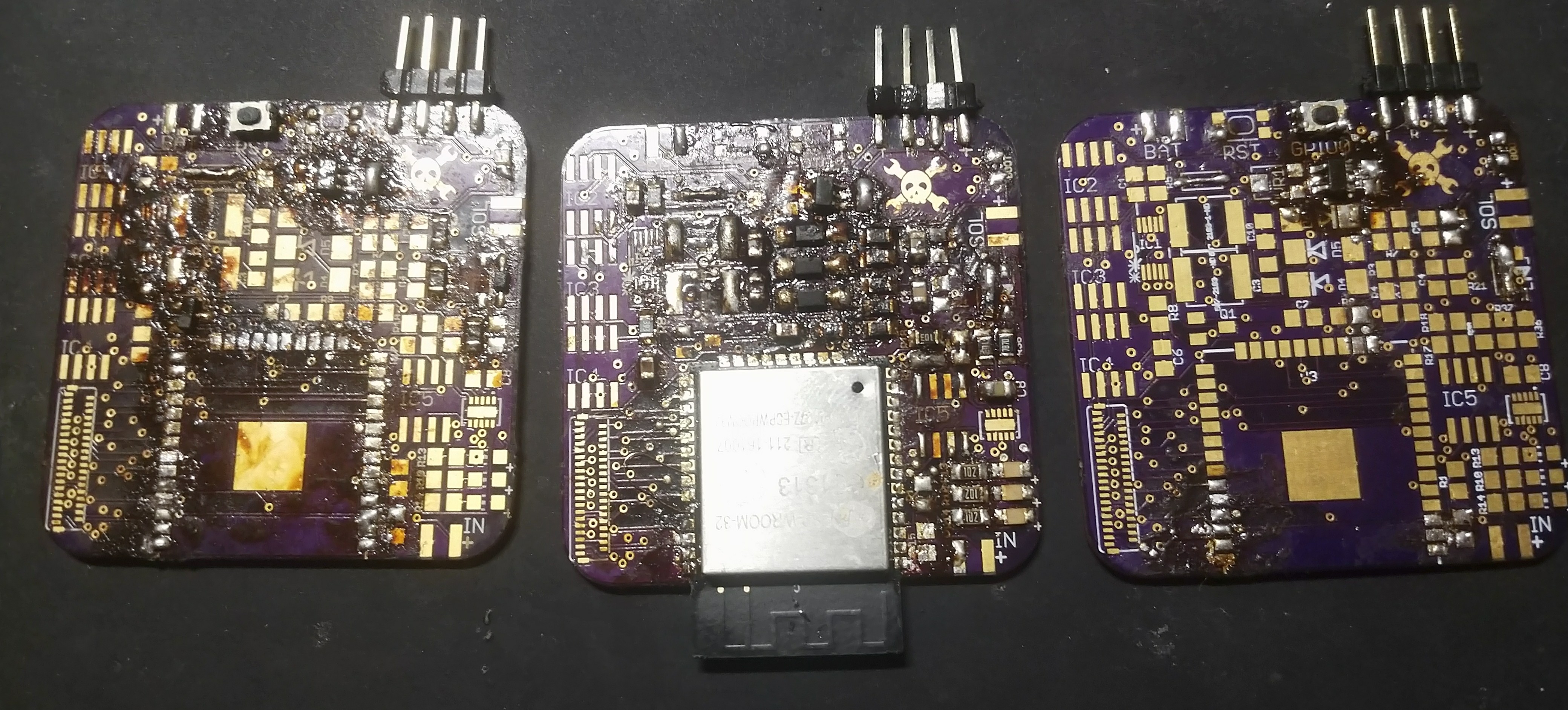
![]()
Basically I soldered up everything, and it did not work. There was a single instance where I was able to program the ESP32 and was getting output on the serial terminal and it was excellent and all was good in the world. However, things went wrong. I accidentally switched the polarity of the power leads (rookie mistake, my bad). Some magic smoke was let out of the regulator but when I tested it on the ol' multimeter things seemed like it was in order: still a solid 3.3 volts.
Yet I was getting no output from the serial terminal and could not flash anything. So silly me I bought another ESP32 thinking that I had toasted the brain. When I replaced the ESP things still didn't work and suddenly my regulator was spitting out 4.8 volts to the ESP. Much too spicy for the ESP (arguably).
So I soldered things on different boards and yadda yadda with limited improvements with my results. I have checked the continuity on all the important traces and everything checks out. If anyone would like to help me out with this PLEASE PLEASE PLEASE send me a message. I have been working on this thing for so long (millennial time are kinda like dog years) and I still haven't gotten even the correct voltages for the e-ink screen.
If anyone would like to offer ANY help in terms of pcb design please please please send me a message and we can chat. Until then I think that I am going to try to make a mk3 pcb which will be a little more robust. See you guys next time.
-
PCBs are a Mess
10/25/2017 at 02:16 • 0 commentsSo the last few months I have been messing around with getting the actual PCB populated with all of the components and such. Things did not go well. While I was trying to make the weird voltages I couldn't figure out why the correct voltages weren't coming out of the LT1945. Of course I thought the chip might be at fault, not my own incompetence. In the process of desoldering and replacing the chip I ripped up a few traces off the board. This is a 10-pin MSOP package....fixing this wasn't possible.
I found out what the issue was though. Shoulda just looked at the dang datasheet....
Why it didn't occur to me check for an enable pin this device. Lesson learned - read the dang datasheet.
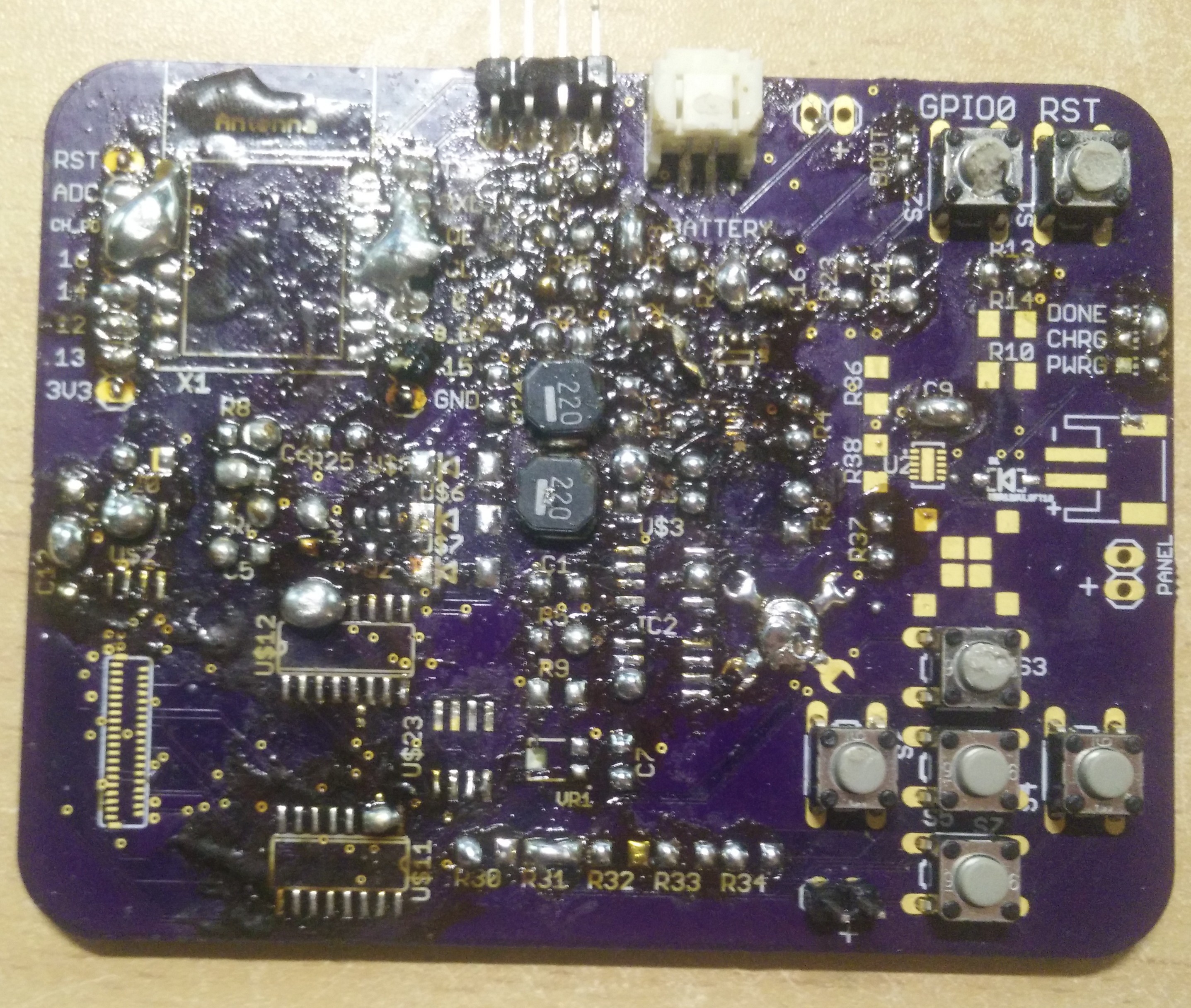
Long story short. I had to desolder all of the components from one PCB to another PCB - thus destroying more components with tiny little legs in the process -_- . Below you can see the resulting carnage and product of my endeavours.
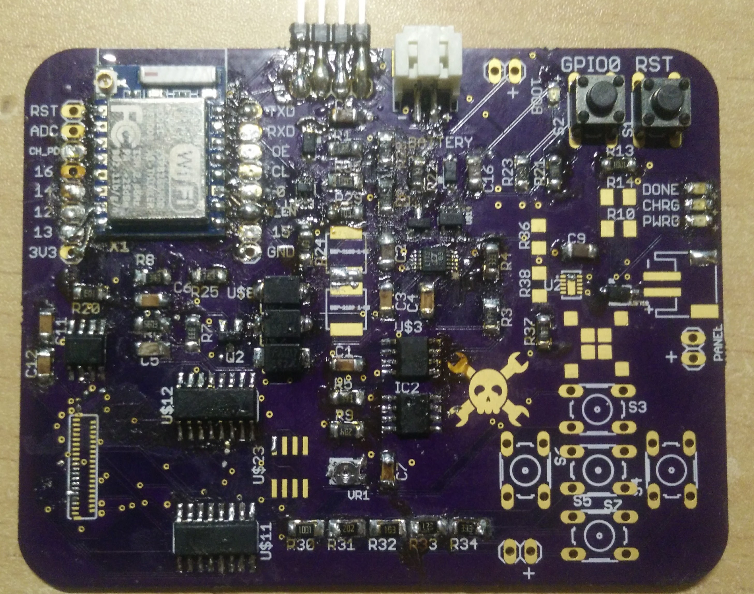
The Second PCB with all of the components transferred onto it
![]()
The original pcb with all of the nasty desoldering carnage
![]()
So after all this my conclusion is... Start a new PCB. There has been some development with ESP32 and e-ink interfacing so I don't think it makes much sense to keep battling a board that will be outdated before it is even working.Within the next few weeks I will be starting a new PCB centered around the ESP32. It will be harder better faster stronger etc. Until then - check yah later.
-
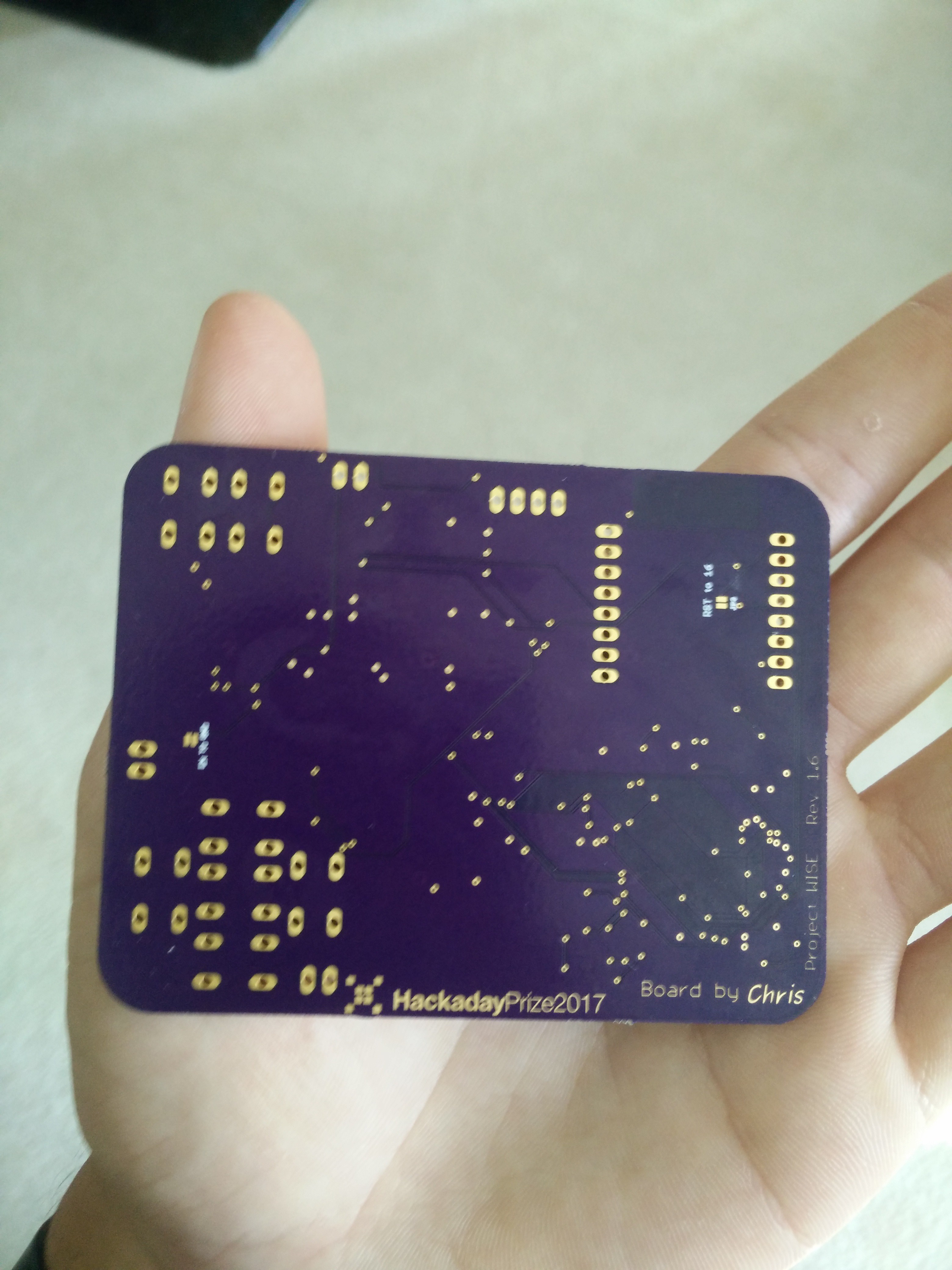
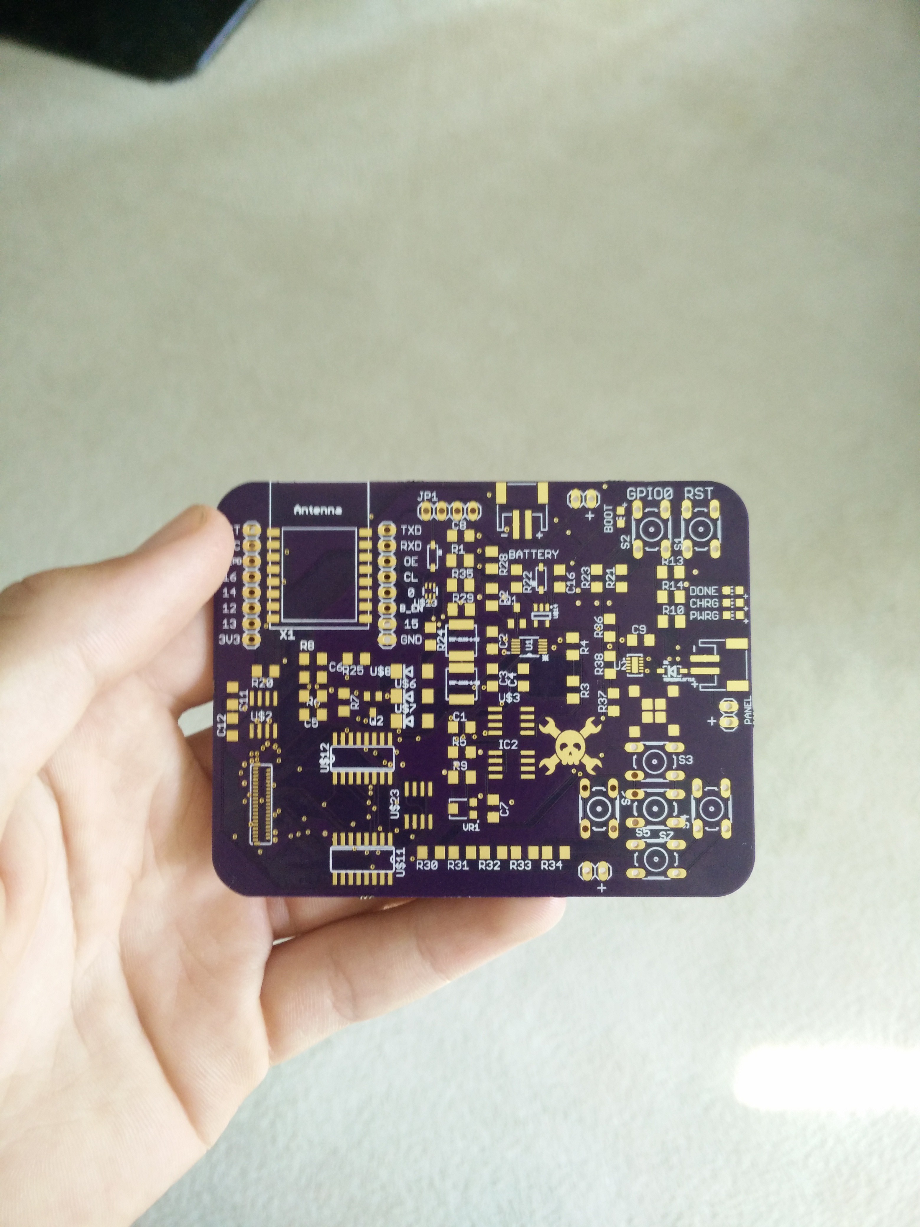
The PCBs came!!
08/17/2017 at 00:58 • 0 commentsJust a quick update, the PCBs came today! They look awesome and I love how well the Jolly Wrencher came out!
![]()
![]()
-
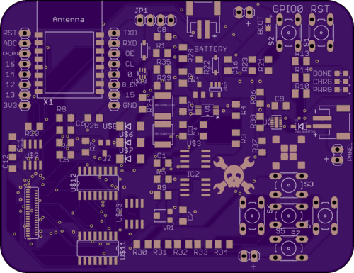
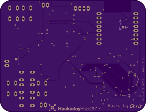
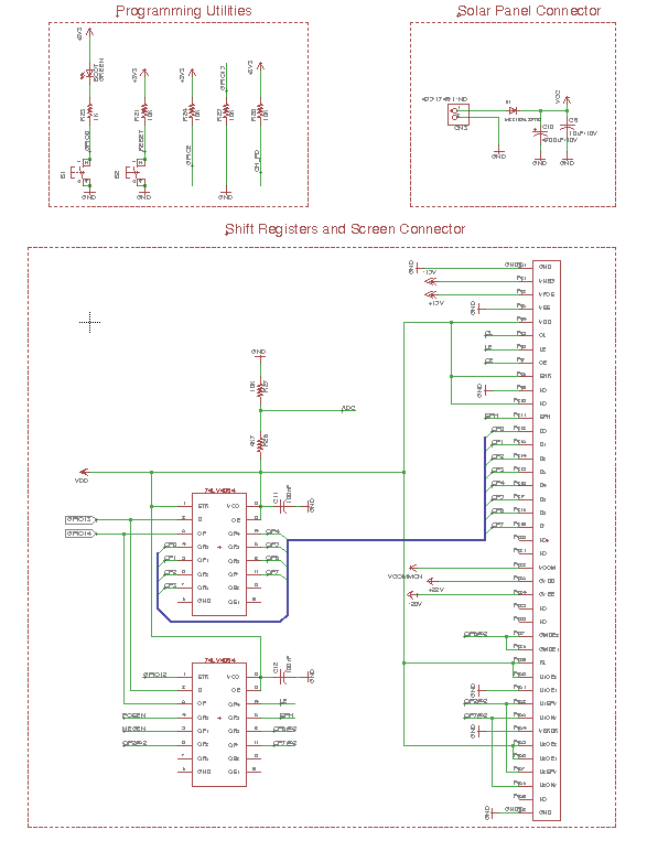
Final Rev 1.5 Schematics and PCB
08/10/2017 at 01:36 • 0 commentsAfter some time, here it is! These are the finalized Rev 1.5 schematics and pcbs!
I will start with the most exciting picture which is the pcb as it will be seen hopefully in real life (render from oshpark obviously).
![]()
![]()
Overall the design isn't very complex and I choose mostly 1206 size smd components for easy hand soldering and hacking when things inevitably go wrong. In the next revision of the board I will probably move to 805 size components which will help lower the cost of the boards a bit.
Below you can see what the pcb looks like in Eagle and it is pretty different from the first version I posted here.
![]()
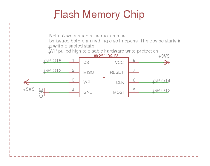
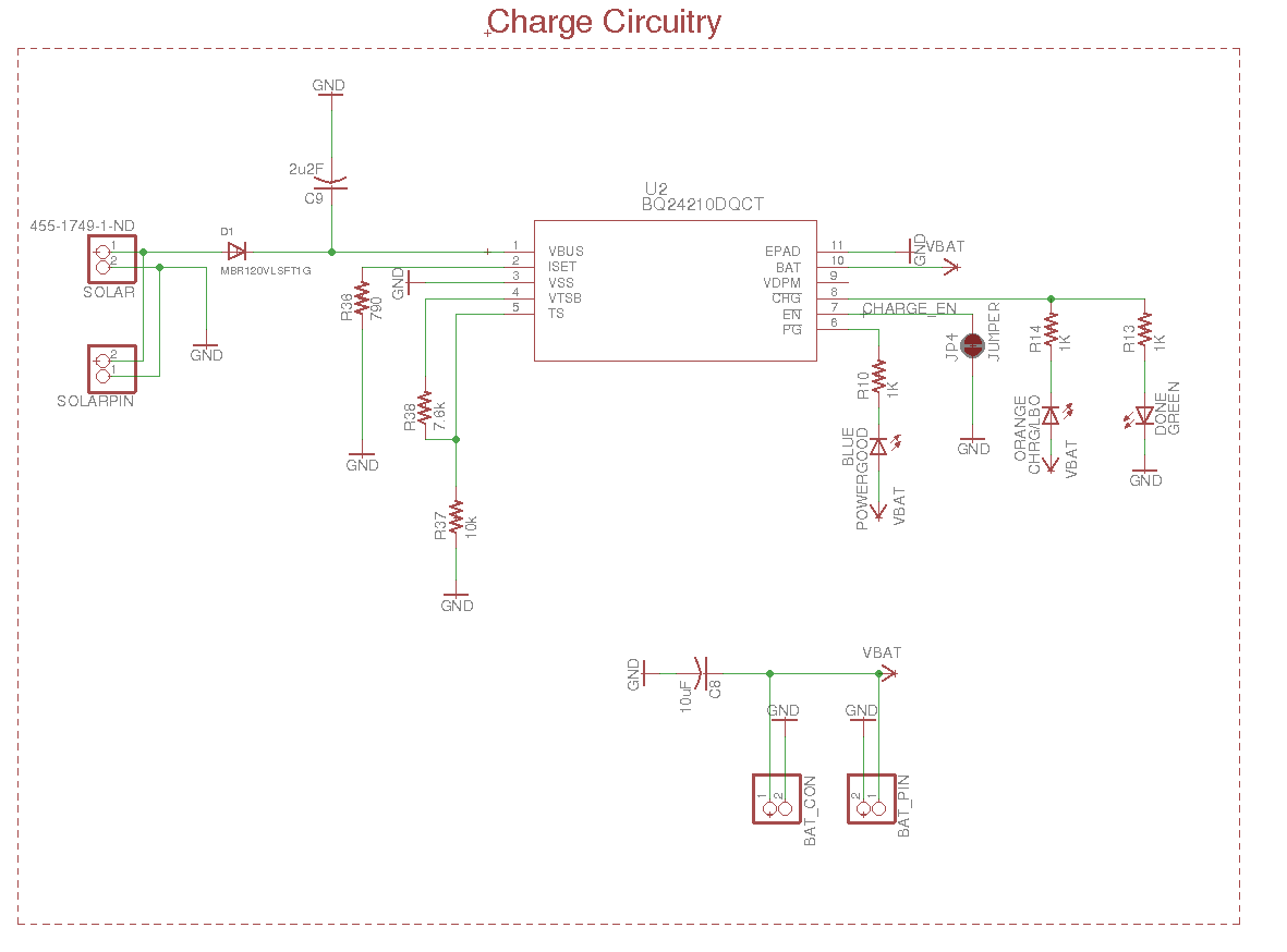
The two biggest changes are the addition of a flash memory chip and the use of a different solar Li-Po charger. These can be seen in the schematics below. Other than a few different bug fixes the schematics between Rev 1 and Rev 1.5 are mostly unchanged.
![]()
I selected a chip with only 32MB of storage to keep the cost down for now. I figure that this is still enough to hold a handful of books and will hopefully be easy enough to upgrade. I have never used flash memory so this will be a good learning experince for me.
![]()
The other major change was the implementation of BQ24210DQCT Li-Po charger. The previous charger I was using was basically a copy of an Adafruit solar-LiPo charger IC but that required a monster 4000uF capacitor so that wasn't really going to work. This chip is much smaller and seems more suited to the task.
I will also be posting the updated BOM via Findchips and will post pictures when I recive the board! I am pretty sure that I failed to correct many wiring mistakes but that is just how you learn, right?
-
Semi-Final Wiseboard PCB
07/02/2017 at 13:24 • 0 comments![]()
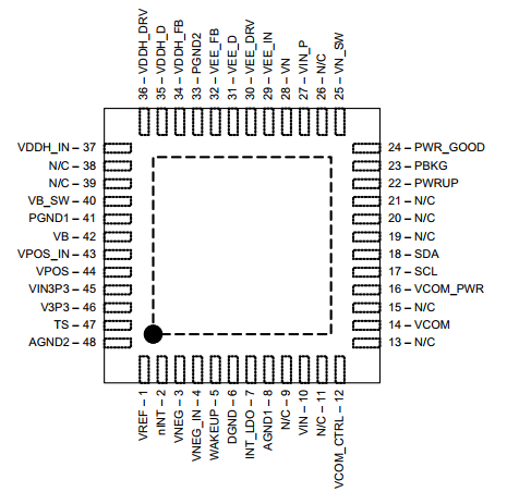
So here we go, the first reveision of the PCB of the wiseboard. Now you will notice that is there is still a handful of airwires to the ground plane. I didn't feel that it was worth the trouble considering that I found the TPS65186 from the WiFi Epaper project here on hackaday.io. This chip is an all in one power supply chip that is cheaper and more capable than buying all of the separate chips that would otherwise generate the voltages required.
This chip has all sorts of bells and whistles and is entirely configurable over I2C. Hopefully I will be able route the whole thing with a 6mil trace width. More to come!![]()
-
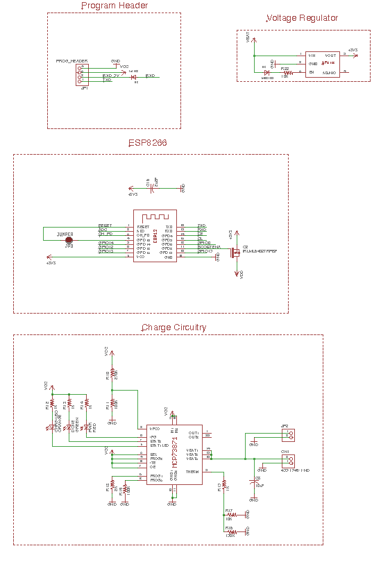
Final Mk1 Schematics!
06/11/2017 at 04:44 • 0 comments![]()
![]()
![]()
So as promised (better late than never) here is the first revision of the schematics. I based the design very heavily off the work of [sprite_tm] with a few simple modifications of my own. Additionally I swapped out the charging IC with one capable of handling solar charging. It is pretty expensive.
One of my favorite little tricks that I used was in regards to the single ADC on the ESP8266. I needed to sense both battery voltage and the resistance of my input buttons. In order to get around the limitation imposed by one ADC I am using a analog switch IC. So when I need to sense battery voltage all I need to do is briefly toggle the switch.
I am sure that I hooked something up wrong; this is the most complex schematic I have ever made. If anyone would like to double check my work please let me know! The eagle .sch will be available below in addition the BOM on findchips.com
-
Schematic Update
05/24/2017 at 02:05 • 0 commentsJust thought I would give another quick update. The schematics are still being created but they are in the home stretch. For now please gaze upon this wonderfully artistic outline of the schematic. It's not much but it's what I have for now. As soon as the real schematic is finished I will post it. After that it will be a PCB and components and hopefully we will have something that at least sort of works!
This is the most complex project I have taken on thus far and I have to say that I am learning a lot. It is a bit scary to think that this may not work the first time around but I guess that is part of the fun, right? If anyone would like to take a once over my schematics and board files before I have them shipped off please send me a message! Until then, enjoy this wonderful picture.
![]()
-
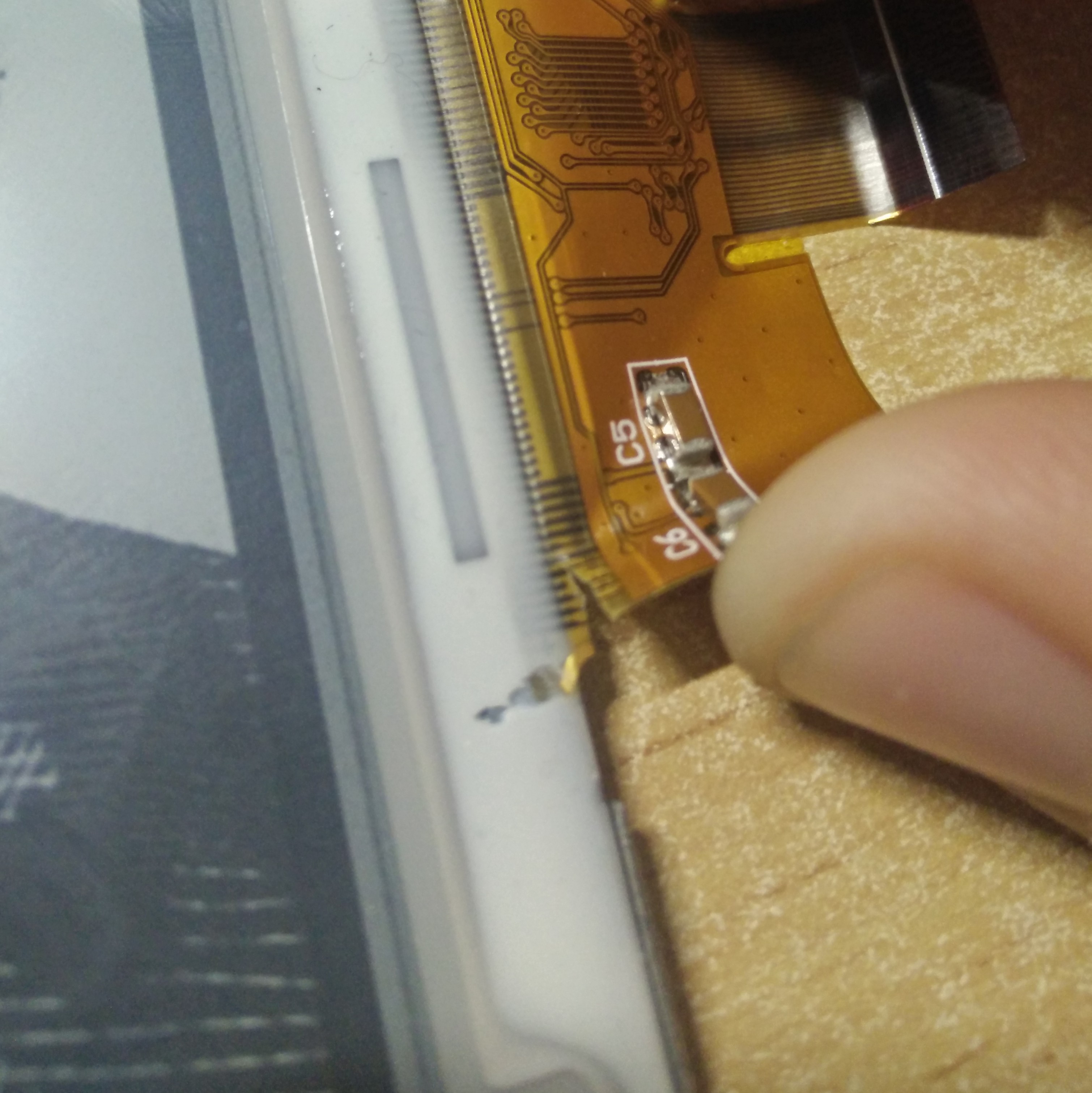
Ripped Ribbon Cable and Slow Progress
05/15/2017 at 01:45 • 0 commentsFinals are almost over which means more time for projects! Yay! I have been working on the schematic and the BOM for this first prototype, albeit slowly. One of the first things that I ordered was the eink display (ED060SC4). Now for those of you keeping score at home you, will recognize that this is the same display that [sprite_tm] used in their wifi-whiteboard project. The bad news is that it was accidentally routed to the wrong address and after some futile attempts to intercept the package I had no choice but to let nature take it's course.
Eventually that package arrived but unfortunately the bottom of the ribbon cable was torn! I have contacted the seller and hopefully will be receiving an exchange soon.
![]()
Within the next few days I hope to have the BOM and pcb finalized so I can actually start melting some solder!