-
New project on Hackaday: NeuronZoo
01/05/2017 at 15:38 • 0 commentsThere was not much activity here lately, because I was working on a new project called NeuronZoo ! The NeuronZoo project is on Hackaday now ! It is a online 3D simulation of (hypothetical) programmable brain cells !
-
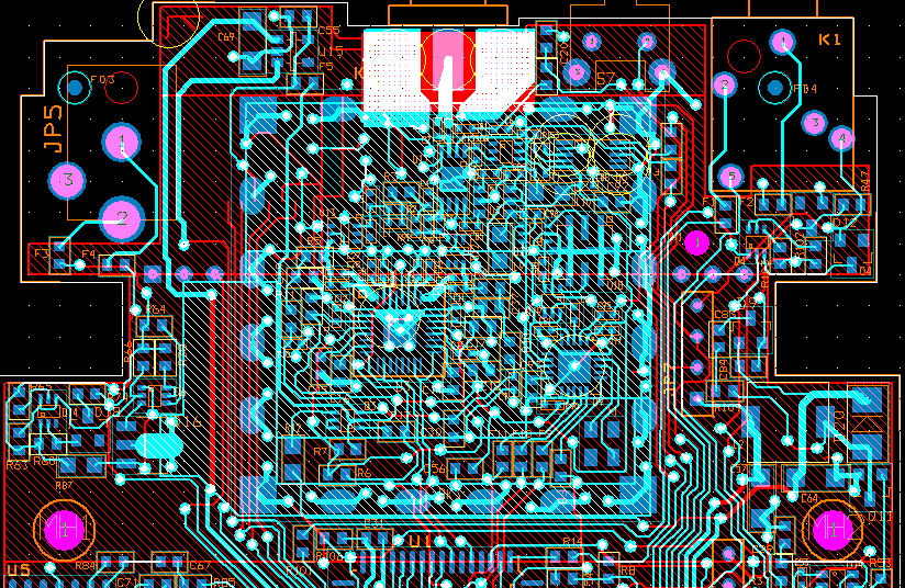
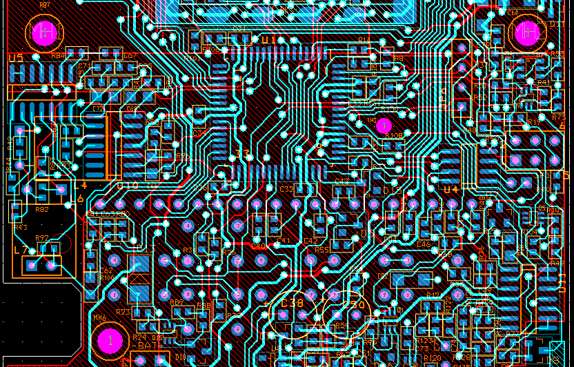
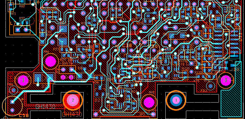
Proto 2 PCB impression
09/28/2014 at 15:35 • 0 commentsThe PCB was designed in Orcad.
In the following screenshot images, the top layer is blue, the bottom layer red. Both layers have ground planes with several traces in it. For better visibility, the ground planes are displayed as a shaded area. (The ground planes have several adjacent sections. The borders between sections look like a normal trace, but they are not !). Note that a shield can be soldered at the RF section.
Upper section:
![]()
Middle section:
![]()
Lower section:
![]()
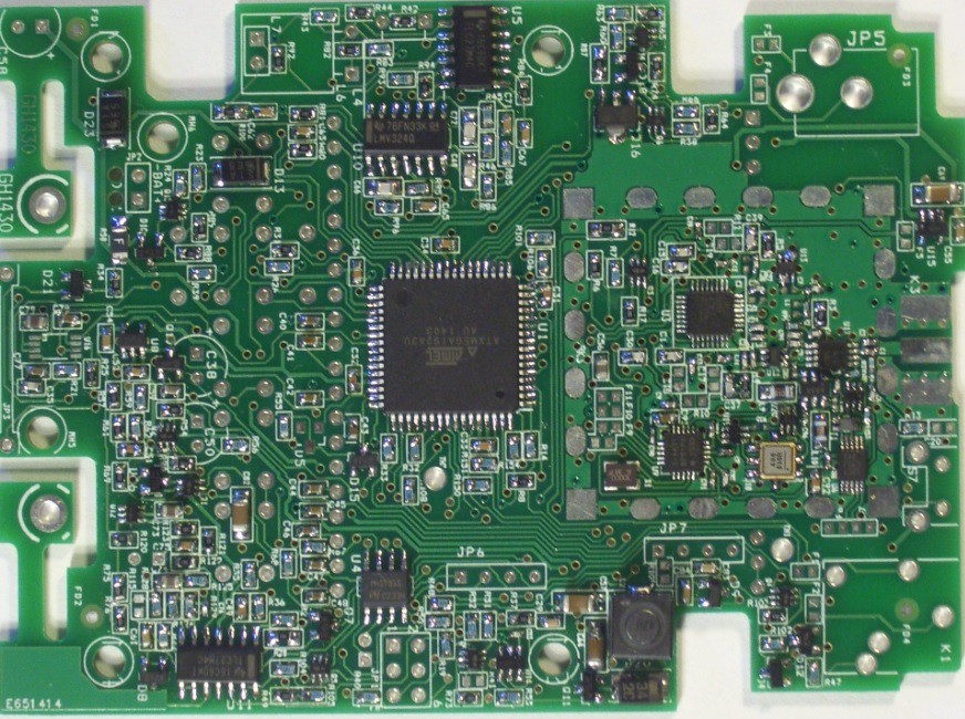
And here is a photograph of the new pcb:
![]()
The assembly of this new pcb is almost finished.
-
Documentation upload
09/21/2014 at 19:37 • 1 commentToday I added links to the (updated) documentation.
It documents the new proto-2 version schematics and pcb (with SAW filter). It also has the newest firmware version (V55) that communicates with the PC application, programmed in Tcl (latest version, 6, provided).
It has pcb Gerber files and assembly drawings. The new BOM includes placement coordinates for the components.
These docs should be enough to duplicate the project !
-
Low cost version
09/18/2014 at 21:07 • 0 commentsSeveral people asked if they can buy the analyzer as a pcb or kit.
I think with more than 270 components, this will be relative expensive and/or quite difficult to assemble. I also think that for most people, the spectrum analyzer itself is the most important, and they don’t need the other features.
------------------------------------------
To make it interesting for a lot of people, the following needs to be done:
- The cost should be low. So it should be a kit.
- It will only be a spectrum analyzer
- The kit should have no more than approx. 60 components to make it easy to build.
- SMD components should not have a very fine pitch
- The ATXMEGA should come pre-programmed, so an AVRISP2 programmer is not needed.
My plan is, to make a 'bare bones' version, and offer it as a kit. But the full version with all options will also be available, perhaps only as complete device.
------------------------------------------------
The bare-bones kit will contain:
- pcb with the programmed ATXMEGA
- All spectrum analyzer components
- The Si4431 (that is difficult to mount) on a pre-assembled small pcb
- connectors: SMA input, 3.5mm RS232 half duplex, connector for 5V power adapter
- on/off button (or .perhaps only a reset button)
- NO lcd and no control buttons. Operation by the PC application.
The price of the bare bones version should be below USD 100, I think.
-------------------------------------------------
The following components can then be mounted as an option:
- LCD with backlight, and control buttons (enables operation without PC)
- micro-SD card connector, real time clock
- battery circuits, step-up converter, charging circuit.
- Enclosure
- Firmware updates by SD-card (no programmer needed).
-----------------------------------------------
The barebones version will require a redesign of the pcb, aimed for easy assembly. For instance, the MBT3946 fine-pitch dual-transistors should be replaced by SOT23 single transistor types. Only a few types of resistors and capacitors should be used. The ATXMEGA has 0.8 mm pitch, that is not very difficult to mount. (It was deliberately chosen for this, I don't like soldering big 0.5mm pitched parts). The Si4012 is a 0.5mm part, but has only 10 pins, si it can be mounted without too much trouble.
It will, however, not be possible to have the barebones design ready before the next judging round of THP...
-
PC remote control application
09/16/2014 at 18:37 • 0 commentsThe analyzer has a RS232 port, intended for remote control. So I created a PC application to control the spectrum analyzer. A simple protocol is used to communicate over this connection, at 38400 bps.
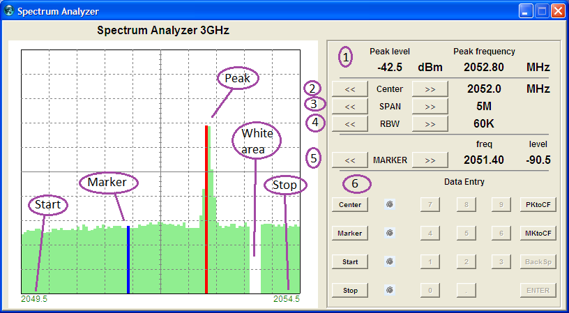
The following screenshot shows the PC application.
![]()
The measurement graphics are show in green. The data is written from left to right. The indicated white area is the separation between new and old data: data to the left of this area has just been written, and data to the right of this area is old and will soon be overwritten (so the white area moves from left to right).
The device finds the peak in the data, displays its level and frequency at (1), and displays the peak position as a red line.
To find level and frequency of other points in the data, you can can move the blue marker with the two marker buttons at (5), and the level and frequency are displayed at the right side of the marker buttons. The marker buttons have a auto-repeat function.
Most important controls are:
(2) Center: Step the center frequency up or down in 1/2-span steps
(3) Span: Select the frequency difference (stop - start) from a series of fixed values.
(4) RBW: Select the resolution bandwidth from a series of fixed values.
The values Center freq, Marker freq, Start and Stop freq can also be directly entered as a number. Just press the button at (6), the associated 'LED' will light up, the number buttons will be enabled and you can enter the number. The entered number will appear above the LEDs (not shown). Press ENTER when you're done.
If you enter start and stop frequency, the span will automatically be set to the difference between start and stop. Using one of the span buttons afterwards will let the span jump back to one of its normal fixed frequency values (1-2-5 sequence). After a span adjustment, the center frequency will stay the same.
All PC software functions are also available on the device itself (sometimes you need to press one or a few buttons more)
The PC software is based upon the Open Instrumentation Project. It is programmed in the script language Tcl/Tk. The use of Tcl means that the application will also work on Linux and on the Mac without any change (but I did not test that...).
I did not program in Tcl before, but the basic functions were not difficult to understand and quite easy to do, and my program is not complicated. Whenever you press a button, a simple code is sent to the analyzer, and the analyzer sends back what numbers and lines are to be displayed on the PC application.
-
Source code
08/20/2014 at 20:36 • 0 commentsToday, I got a mail from Hackaday, telling that I should also put my sourcecode on the project page.
I am afraid that the sourcecode is not an easy read. It is based on software from older projects, and it should be cleaned up. I think you can tell from the code that I did quite a lot of assembly coding in the past...
This evening, I translated several dutch comments to English. The real spectrum-analyzer work is in 'sa.c'.
-
Bill of materials
08/19/2014 at 19:30 • 0 commentsI added the BOM (Bill of materials) to the links. This will not be the final BOM. I added it as a Google speadsheet document.
Later this week, the 4 or 5 most difficult parts will be placed on my new pcb (by someone who has the equipment to do that). After that, I will mount the other parts myself.
There are 273 parts at the moment, quite a lot.
I could sell pcb's with all parts mounted when there are enough people who want one (and at least the hardware is final). The pcb could be delivered tested and calibrated.
I could also sell the housing with all holes laser-cut. That reminds me... enclosure and mechanical parts are not yet in the BOM.
-
More about the firmware
08/17/2014 at 21:02 • 0 commentsThe Si4431 and Si4012 each have a private serial connection to the ATXMEGA, it is also not shared with other devices. This gives the possibility to easily move their code from a 'main loop' to an interrupt routine, if this should be needed. An ATXMEGA has plenty SPI and other serial connections, that makes this easy. At the moment, interrupts are not used in this section.
The firmware divides the total frequency span in a certain number of pixels (100 for this display).
It then depends on the selected bandwidth (RBW) how many measurements will be done for each pixel. The Si4431 can be set to a RBW between 2.5 and 600 KHz. This does not mean that this is the spacing between the measurements, a certain overlap is needed. The measurement that gives the highest value will be taken as the value for this pixel.
At a certain frequency, measurements with low bandwidth do take more time, but the difference in time is quite small (not as big as the bandwidth difference would suggest).
Note that in peak detect mode, the detected peak will record the frequency of the highest measurement within the highest pixel, so the frequency resolution of the peak measurement is much better than just one pixel.
- To determine the LO and IF frequency, the following is used:
For RF up to 600 MHz, IF is set to (RF +250MHz) and LO is 250 MHz, so the input RF frequency is LO - IF (fundamental mixing).
For RF between 600 and 1700MHz, IF is set to (RF/2 - 40MHz), and LO is (RF/2 + 40MHz), so the input RF frequency is LO + IF (fundamental mixing).
Above 1700 MHz, 3rd harmonic mixing is used. IF is set to (RF/4 - 60MHz). LO is (RF/4 + 20MHz), so the input RF frequency is (3*LO) + IF.
For each frequency, a second measurement is done, with the LO 40MHz higher (and IF adjusted to give the same RF). The lowest value of both measurements is taken. This will suppress mirror frequencies. For 3rd harmonic mixing it also will suppress fundamental mix results, and for fundamental mixing it will suppress results from higher harmonic mixing.
When the spectrum is crowded, this will not always give the desired result, and a control should be added to change this 40MHz distance.
Of course, the above system to derive LO and IF frequencies will have to change when the SAW filter is going to be used.
-
System diagram
08/16/2014 at 13:43 • 0 commentsThere were some more things that I had do to comply with the prize regulations:
- make the entry official So I did.
- add a system diagram. I added this to the 'details' section today.
- have at least four project logs
The system diagram was made with Excel. You can easily draw boxes around your cells, and your boxes will align nicely. It is also easy to change the size of your boxes to make the text fit. It also lets you use arrows. At the end, I make a screenshot (gridlines off) and let Paint convert it to a graphical format.
In this project log I will explain some sections that have not been discussed in the 'details' section.
- frequency measurement with the RF power detector
The RF power detector chip has 2 identical channels. The input signal is split in two branches: The first branch passes a high pass filter and then goes to the first detector channel. The second branch passes a low pass filter and goes to the second detector channel.
The filters are not very steep. The outputs of the filters will have an amplitude ratio that is dependent on the input frequency, so the input frequency can be recovered by taking the difference of the two outputs of the logarithmic RF detector. Of course, this principle does only work if only a single frequency is present (or if other frequencies are much lower in amplitude).
The firmware uses the output difference to calculate the frequency. It uses a table with calibration points, that is determined for each device individually, and stored in a separate flash section of the controller.
This frequency measurement is also supposed to work for short RF pulses. Therefore, the outputs of the RF detector are routed to the two different ADC's, and the ADC's will sample the signal at exactly the same moment.
The RF detector is not very sensitive, it needs at least -60 dBm, whereas the spectrum analyzer will be able to detect signals as low as -110dB.
- On/Off button
The on/off button is a momentary switch, that will set the electronic power switch in the ON position when pressed.
When you want to switch the device off, you press the on/off button again. This will NOT directly cause the power switch to switch off. But the firmware will notice that you pressed the button, it will wait until you release the button, and will then close the logfile and switch the power off. The firmware can also switch the power off if the battery voltage becomes too low.
The electronic power switch is placed after the step-up converter. By placing it at this position, a voltage drop over the power switch will give us less efficiency loss then if it was placed before the step-up converter. Note that when the power is off, the transistor of the step-up converter is also off, and the step-up converter does not consume any current because its control circuits are powered by one of the linear regulators.
-
First project log
08/15/2014 at 18:06 • 0 commentsA new pcb version, that I did receive from the pcb service today, has small design changes and corrects several small errors, and will also have a SAW filter that can be switched into the IF path. The filter is wide enough (around 5 MHz) that still two RF-IF combinations can be used for mirror suppression (if not wide enough for a certain situation, the SAW can be bypassed). The intention is that the SAW filter can give better selectivity.
The SAW filter can hopefully also filter the false response of the Si4431 away (at about 1.9 MHz next to a peak, it has a second peak that is 30dB lower than the main one).
The firmware still requires much work. Changes must be done for the SAW filter. It might be good to have a few options for the mirror suppression system. I also want to be able to use stored settings. Some logging would also be nice.
The sound recorder is not working yet, I could not reach a good write throughput to the micro-SD card. On a new card it was good, but it seems that as soon as there are other things on the card, write rate drops to around 3 kByte/second. I use a rather slow cpu speed (4 MHz), but I don’t think this is the problem, because I can playback music files at 22050 Hz sample frequency (and they sound very good). I use the famous FATFS from ChaN, and two 1.5KB buffers. Perhaps someone has an advice ?
The sound recorder might also store the screen contents, and show this screen contents when the sound is played back.
When using the device to debug wireless communication, it will be possible to decode the communication in the Si4431 (it has several functions for that) and show the (decoded) contents on the screen (perhaps in a scrollable window). The Si4431 can also transfer the raw FSK or OOK data to the processor.
The frequency of the spectrum analyzer is quite precise, because the Si4431 derives its frequency from a crystal. The Si4012 oscillator has no crystal, but we could measure its output with the Si4431 and then adjust the frequency of the Si4012 if it deviates. The devices do have some phase noise, that might be problematic in some cases. If we assume an IF around 315 MHz (the intended SWA filter frequency), then the phase noise of the Si4012 will be the most prevalent (at high frequencies and in 3rd harmonic mode). We could add a small add-on pcb with a higher quality oscillator if the phase noise is a problem.
