The network analyzer is controlled with a BeagleBone "cape". This board provides power management, reference clock synthesis, and routes IO pins on the BeagleBone to headers for the other modules.
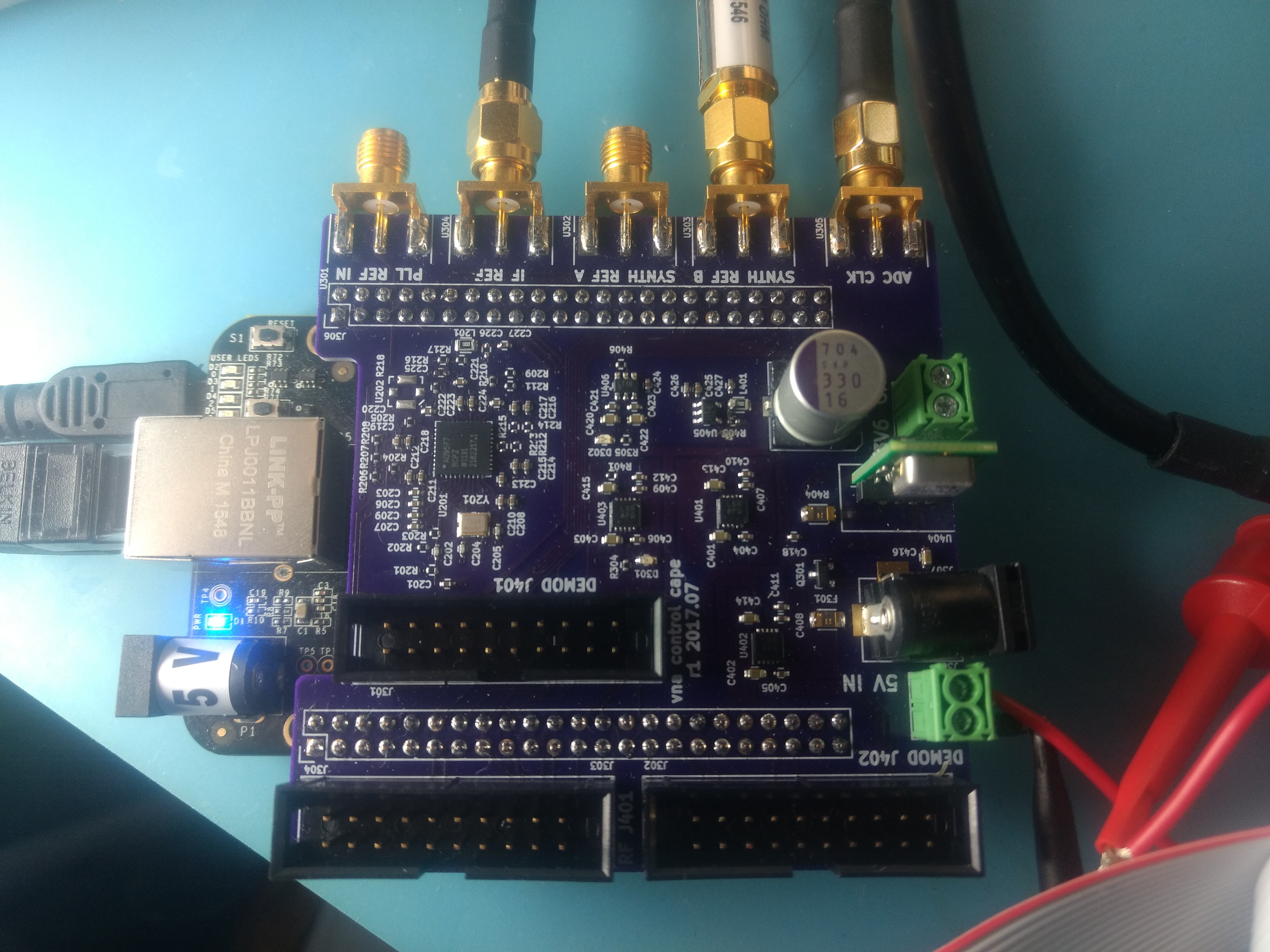
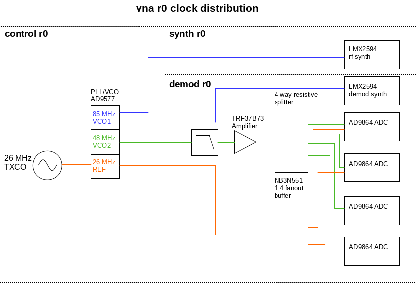
Clocks synthesis is done with an AD9577. Control of this chip is surprisingly simple over I2C, my software (almost) worked on the first try. This chip has two VCOs and PLLs, each with two differential output channels. I'm referencing all the clocks in the signal chain to a single crystal to reduce relative drift between all the clocks. An earlier revision of the VNA had separate oscillators for the RF and LO synthesizers, which made the resulting IF squirrely. The decimation filters on the ADC aren't particularly flat, so keeping the IF frequency stable is important for the stability of measurements.
An on-board The 26 MHz crystal (or an external reference clock) is fed to the PLL/VCO which synthesizes two 85 MHz synthesizer reference signals and a 48 MHz IF-LO tone. The 26 MHz clock is also buffered to provide an ADC reference clock.
A single 5V input powers the network analyzer. The 5V input rail switched directly to the variable gain amplifier on the RF synthesizer board, and taken by switching regulators to create -5 V and 3.6 V rails. Each of the modules has an independent switchable 3.3 V rail regulated with an LDO off the 3.6 V supply. Other than mixing up pull-up/pull-down on enable/power-down lines, all of the power distribution worked without any issues.

Bring-up of the power distribution and clock synthesis were uneventful. The only debugging excitement on the control cape arose from a short between signal lines, possibly due mask containment issue during manufacturing. When testing the ADCs on the demodulator boards I noticed that the values of the sampled signal looked .. strange. Probing with an oscilloscope revealed that two of the ADCs were apparently sending trinary "trits". I suspected that was the result of a battle between output drivers, so I powered down the VNA and located a short on the control PCB with a multimeter.
I didn't see any obvious shorts and the bridge was measurable on an unpopulated board, so I fired up my thermal camera. The short was approximately localized by running a current limited power supply down the two signal lines on an unpopulated board. This heated up the traces and illuminated the path of the current.
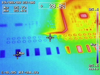
The thermal image narrowed down the short location to the right side of the board near U406.
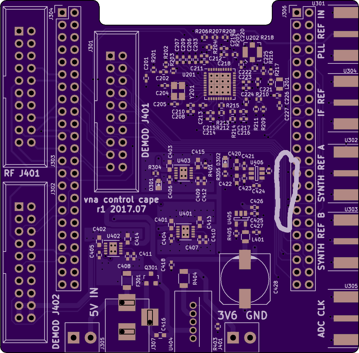
Even knowing where to look I still couldn't spot any bridges so I started hunting with a microscope.
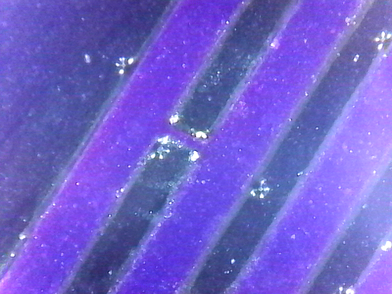 At 250x magnification I spotted a 1 mil thick bridge between the two signal lines. Once I knew exactly where to look I backed off on the magnification:
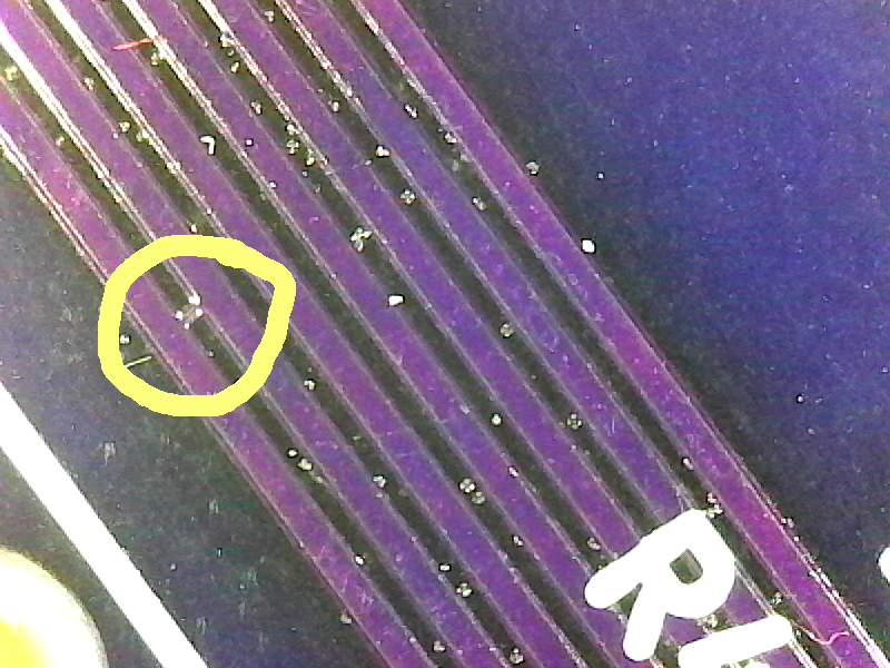
I cut the bridge with a knife then verified that short was eliminated with a multimeter (and checked that none of the other closely packed signal lines had bridges with adjacent traces).
I sent the PCB vendor pictures of the bridge and asked them to isolate where in the process the error was introduced so I could hopefully avoid this in the future. They suspected that it was a mask contamination issue at the fab and immediately issued a full refund for the PCBs without me requesting one. (The short appeared between traces that were right at minimum 5 mils spacing specified by the manufacturer, I'll back off on that a little on future boards if space permits.)
With the copper bridge cut, the VNA control board appears to be fully functional. The next update will describe testing the four channel simultaneous demodulator board.
 Jon Klein
Discussions
Become a Hackaday.io Member
Create an account to leave a comment. Already have an account? Log In.