-
Version E
09/15/2017 at 14:00 • 0 commentsVersion E of the One Bit CPU
I updated the schematic and the PCB of the One Bit CPU.
- I fixed up the two schematic errors.
- Removed the single step (does not work that well)
- Reworked the clock circuit
- Removed some redundant circuity
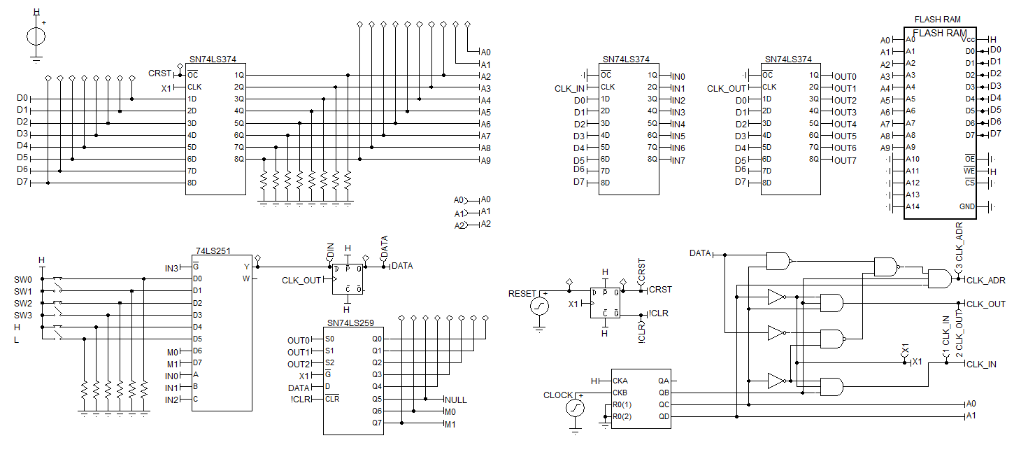
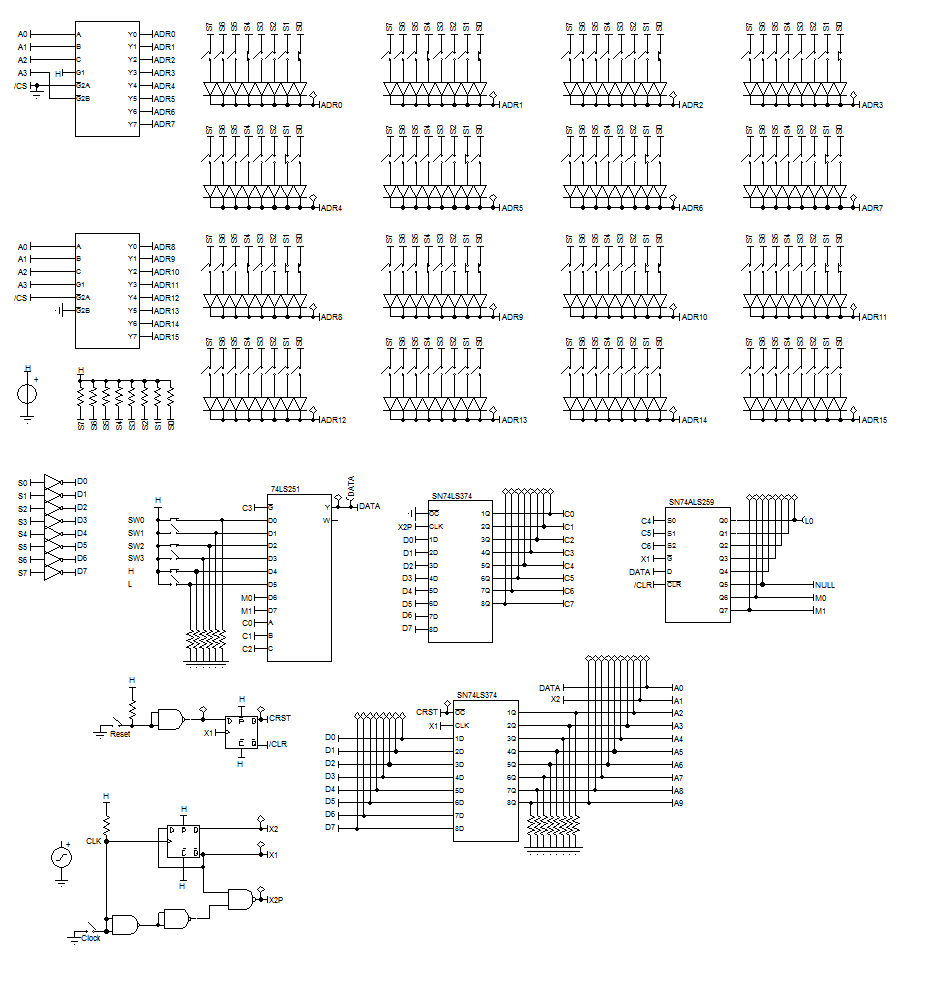
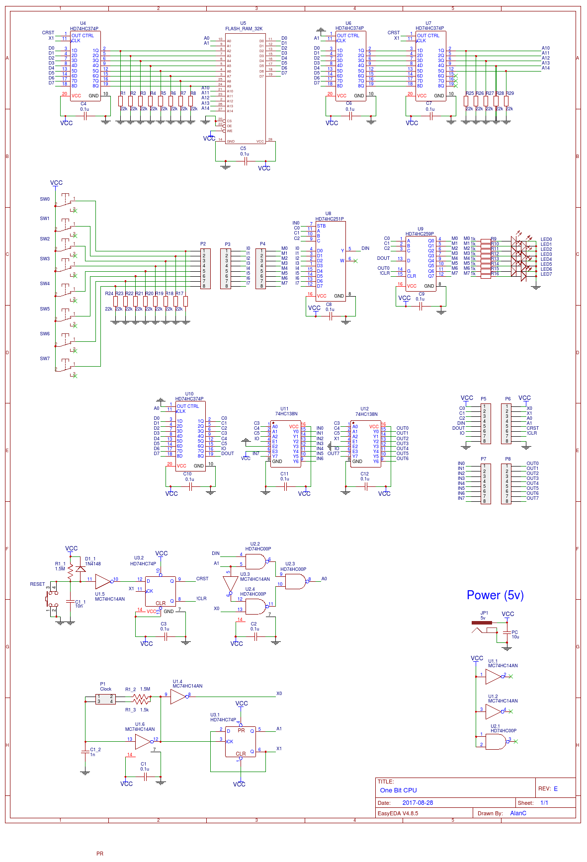
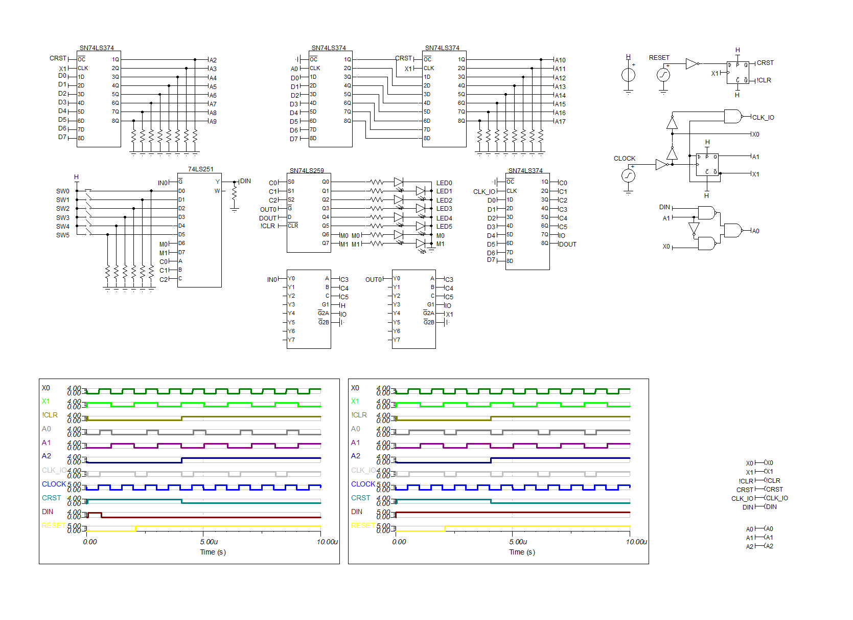
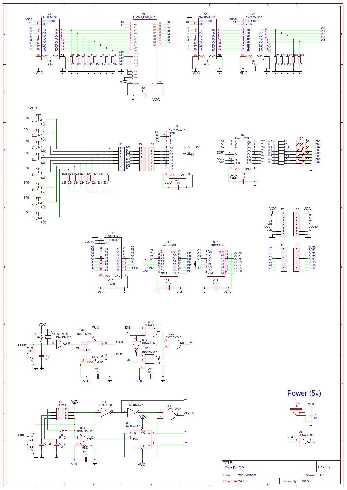
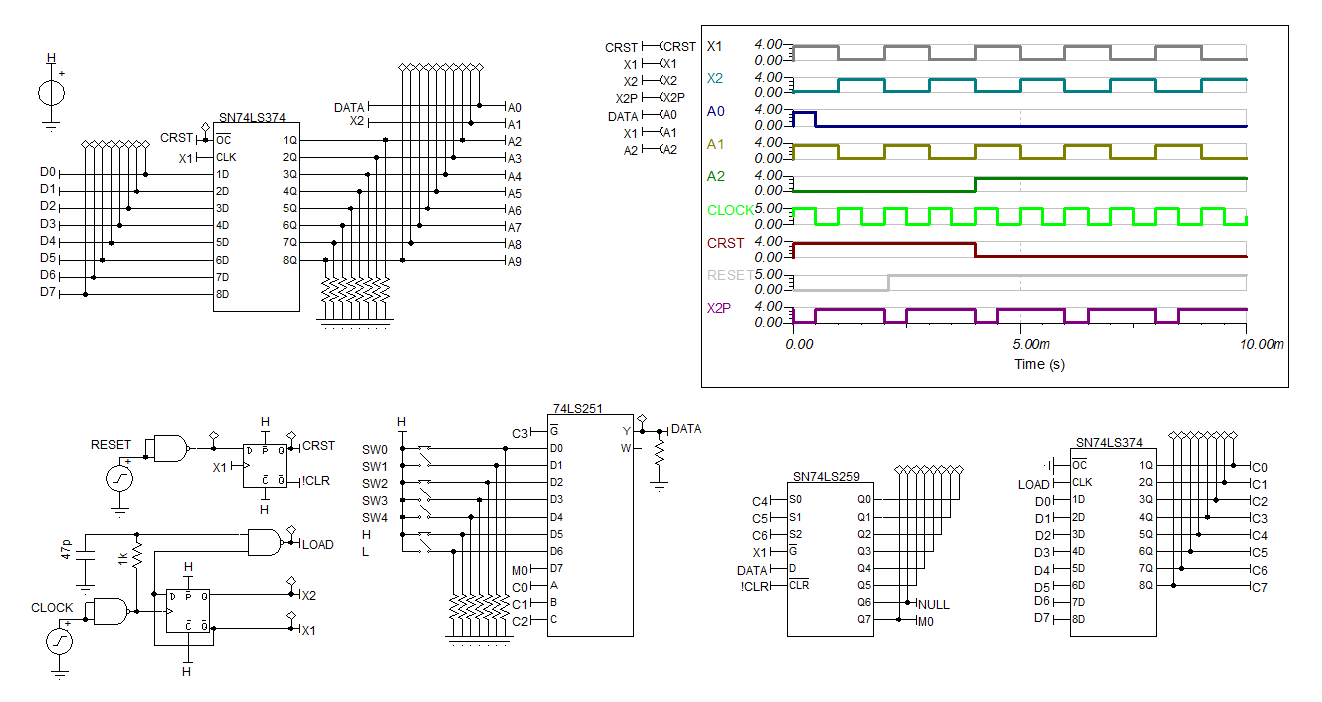
Hers is the updated schematic:
![]()
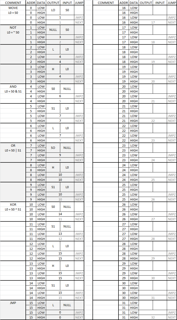
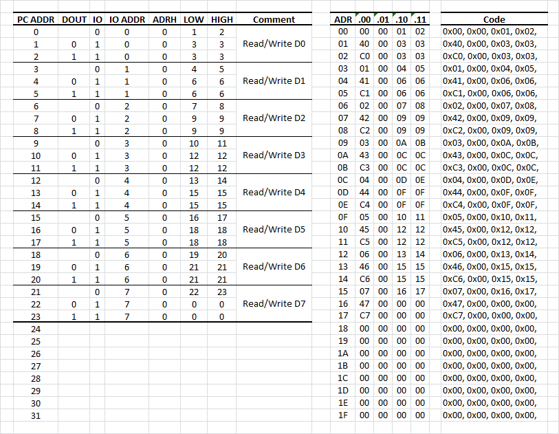
Here is the test program:
Spend a few moments to see that DOUT, IO and IO ADDR are merged into one byte.
- DOUT is ignored for an input (IO=0).
- IO equals 0 for an input and 1 for and output.
- ADDR IO is a 6 bit input or output address.
Th high address (or page) is ADRH.
The low address is either LOW or HIGH depending on the value of DIN (the read value from the selected input).
Each instruction (PC ADDR or ADR) is four bytes, therefore when using a 32k flash ROM it has 8k program space.
You may see that the One Bit CPU is basically a Finite State Machine (FSM).
Demo Program
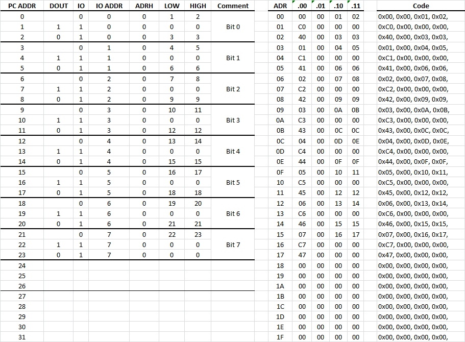
A demo program needs to do something visual. So I coded a binary counter:
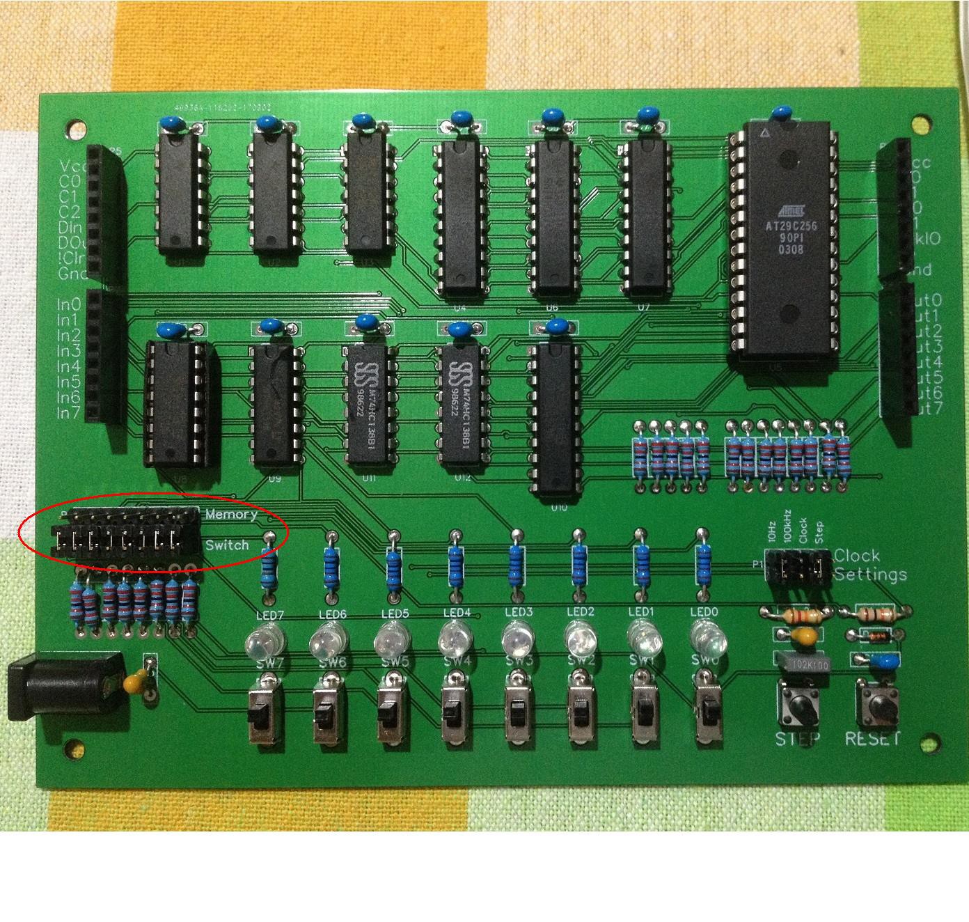
But for this to work all the shunts have to be moved from switch to memory:
With the clock set at 10Hz, it now slow counts away the day.
AlanX
-
FLASH Programmer
09/13/2017 at 12:42 • 0 commentsFlash Programmer
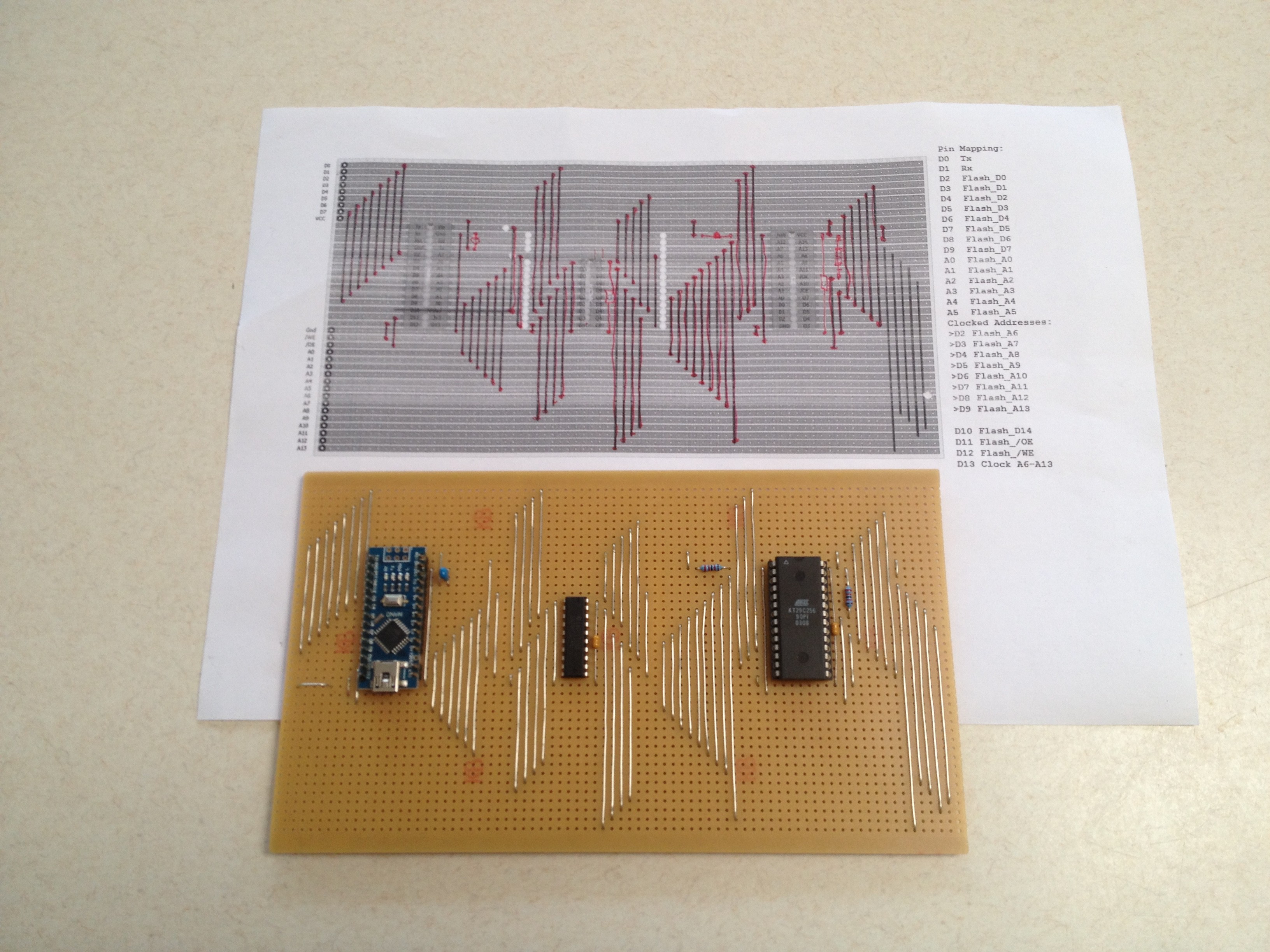
I need a programmer for the FLASH ROM. I designed something in EasyEDA (a PCB fabrication service) but decided strip-board is more appropriate:
I destroyed a RAM chip before due to careless programming (... is there really any other type?), so I added 1k resistors between the Nano databus and the Flash data bus (not shown above). The strip-board has pretty high capacitance which slows down the access time down to about 1 us! Anyway I can read the chip (pretty sure I am reading the chip), and the address latch is working, but I can't get it to write. It's just a matter of time working out why it it not working.
Its a New Day
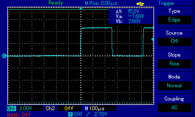
This morning I popped the Flash chip and configured the Nano to count, databus and then address bus with and without !WE. The maximum frequency was 178kHz. All the data lines and address lines had the correct frequency. The only problem I found is that 1us (program) delay was about 120ns!
![]()
Using "delayMicroseconds(2);" gives me about 1us:
![]()
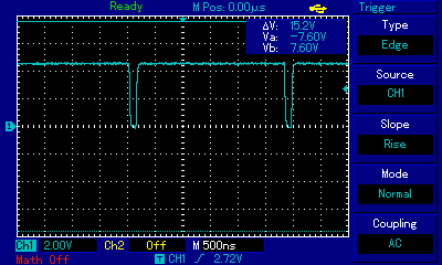
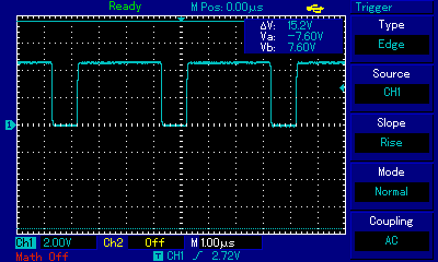
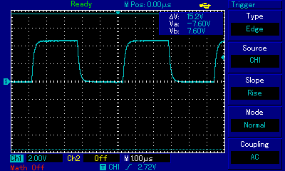
As I added 1k resistor to the databus to protect against bus conflict (or bad programming), I expected the bus to slowdown. Here is is on the Arduino side:
![]()
And on the Flash side (with the chip re-installed):
![]()
Thus the need for the 1us wait for the databus.
Remember that it is only the programmer that has the protective resistors so the slow down is not material.
The supply voltage is about 4.7v which is good enough, so I conclude the board is functional, back to codding errors.
Polling
The AT29C256 allows polling during the write cycle. It returns the complement of the last byte written. The table below shows the byte written|Read:
0000: 00|FF 01|BF 02|FF 03|BF
0004: 04|FF 05|BF 06|FF 07|BF
0008: 08|FF 09|BF 0A|FF 0B|BF
000C: 0C|FF 0D|BF 0E|FF 0F|BF
0010: F0|7F F1|3F F2|7F F3|3F
0014: F4|7F F5|3F F6|7F F7|3F
0018: F8|7F F9|3F FA|7F FB|3F
001C: FC|7F FD|3F FE|7F FF|3F
0020: 00|FF 01|BF 20|FF 30|BF
0024: 40|FF 50|BF 60|FF 70|BF
0028: 80|7F 90|3F A0|7F B0|3F
002C: C0|7F D0|3F E0|7F F0|3F
0030: 0F|FF 1F|BF 2F|FF 3F|BF
0034: 4F|FF 5F|BF 6F|FF 7F|BF
0038: 8F|7F 9F|3F AF|7F BF|3F
003C: CF|7F DF|3F EF|7F FF|3F
Its garbage! "FF" should return "00" not "3F".
Okay swap out the chip (it was a bit suspect as it has scratches on it - is it new?).
WTF! It works, this is the second run where I over wrote my first success:
Welcome to the AT19C256 FLASH Programmer V1.0
First read the FLASH (y/n)?
0000: 00 01 02 03
0004: 04 05 06 07
0008: 08 09 0A 0B
000C: 0C 0D 0E 0F
0010: F0 F1 F2 F3
0014: F4 F5 F6 F7
0018: F8 F9 FA FB
001C: FC FD FE FF
0020: 00 01 20 30
0024: 40 50 60 70
0028: 80 90 A0 B0
002C: C0 D0 E0 F0
0030: 0F 1F 2F 3F
0034: 4F 5F 6F 7F
0038: 8F 9F AF BF
003C: CF DF EF FF
FLASH read done.
Write the FLASH (y/n)?
FLASH write done.
Verify (read) the FLASH (y/n)?
0000: 00|00 00|00 00|00 00|00
0004: FF|FF FF|FF FF|FF FF|FF
0008: 00|00 00|00 00|00 00|00
000C: FF|FF FF|FF FF|FF FF|FF
0010: 00|00 00|00 00|00 00|00
0014: FF|FF FF|FF FF|FF FF|FF
0018: 00|00 00|00 00|00 00|00
001C: FF|FF FF|FF FF|FF FF|FF
0020: 00|00 00|00 00|00 00|00
0024: FF|FF FF|FF FF|FF FF|FF
0028: 00|00 00|00 00|00 00|00
002C: FF|FF FF|FF FF|FF FF|FF
0030: 00|00 00|00 00|00 00|00
0034: FF|FF FF|FF FF|FF FF|FF
0038: 00|00 00|00 00|00 00|00
003C: FF|FF FF|FF FF|FF FF|FF
FLASH verify done.
FLASH Programmer done.
I am a happy little flash programmer now.
AlanX
-
Version D
09/01/2017 at 05:23 • 0 commentsVersion D
Still paying with the design, usually this means that the design is not done.
It's just something you know and can not explain, i.e. "You can do better!".
So yes, Version D is much better:
![]()
Improvements:
- Used the spare I/O byte as page memory (cost two chips), I can now access all the memory on the PEROM (that what the datasheet calls the Flash memory).
- Used bit 7 of the IO byte to set the output high or low rather than read a high or low input.
- Used bit 6 of the IO byte to determine if the I/O is read or write (cost two decoder chips).
- So I can read and write up to 64 inputs and outputs (base board has six inputs and outputs and two memory bits).
- The design is very simple!
- For the PCB design I can add a port for expansion of additional I/O as required.
The timing diagrams basically show the relationship between the signals, the address decode based on DIN high or DIN low and that the signals are glitch free.
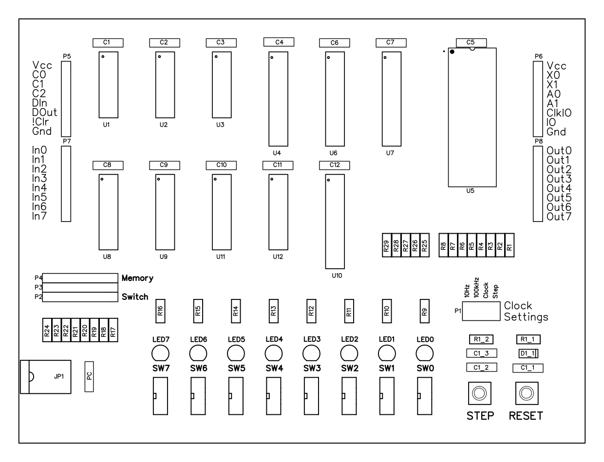
PCB
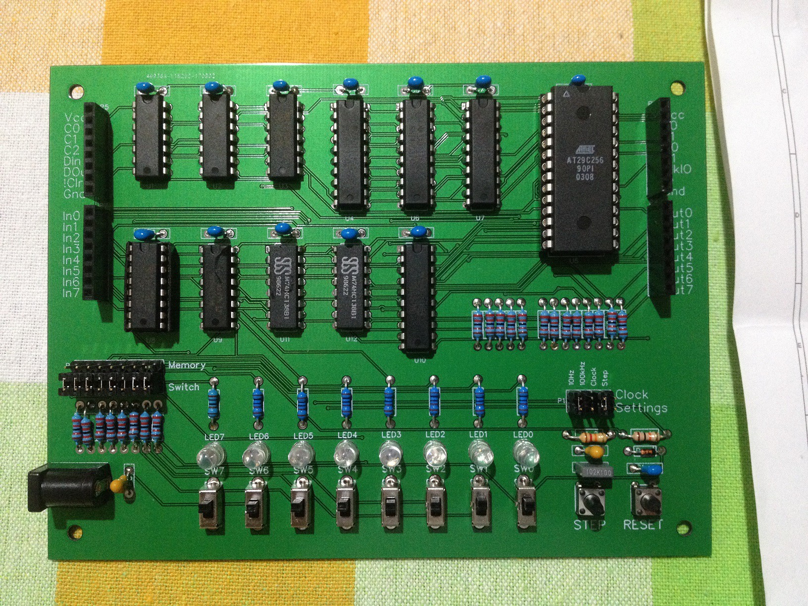
For the PCB I have used jumpers to switch between memory bits and input switches, and provided expansion ports (... well you never know!). The PCB was a bit of a rush last night so the layout could be improved but it is been fabricated now:
![]()
Here is the schematic:
![]()
Including postage the PCBs (for five) cost US$33, you cannot complain other than I only really want one PCB.
Assembled and Waiting a Programmed Flash ROM
Here is the assembled board. I must have been in a rush as the components are all over the place!
![]()
AlanX
-
Strip-Board Design
08/30/2017 at 13:34 • 0 commentsStrip-Board Design
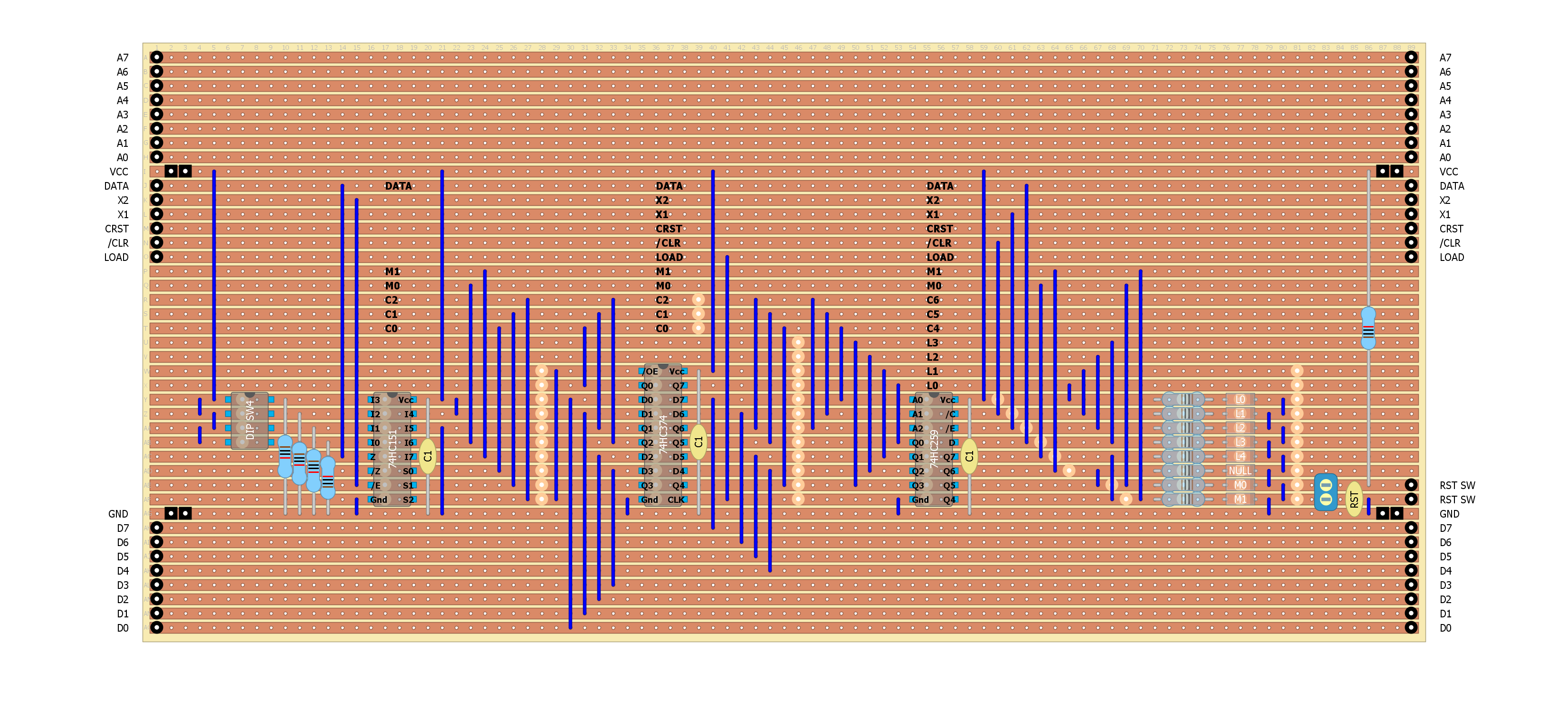
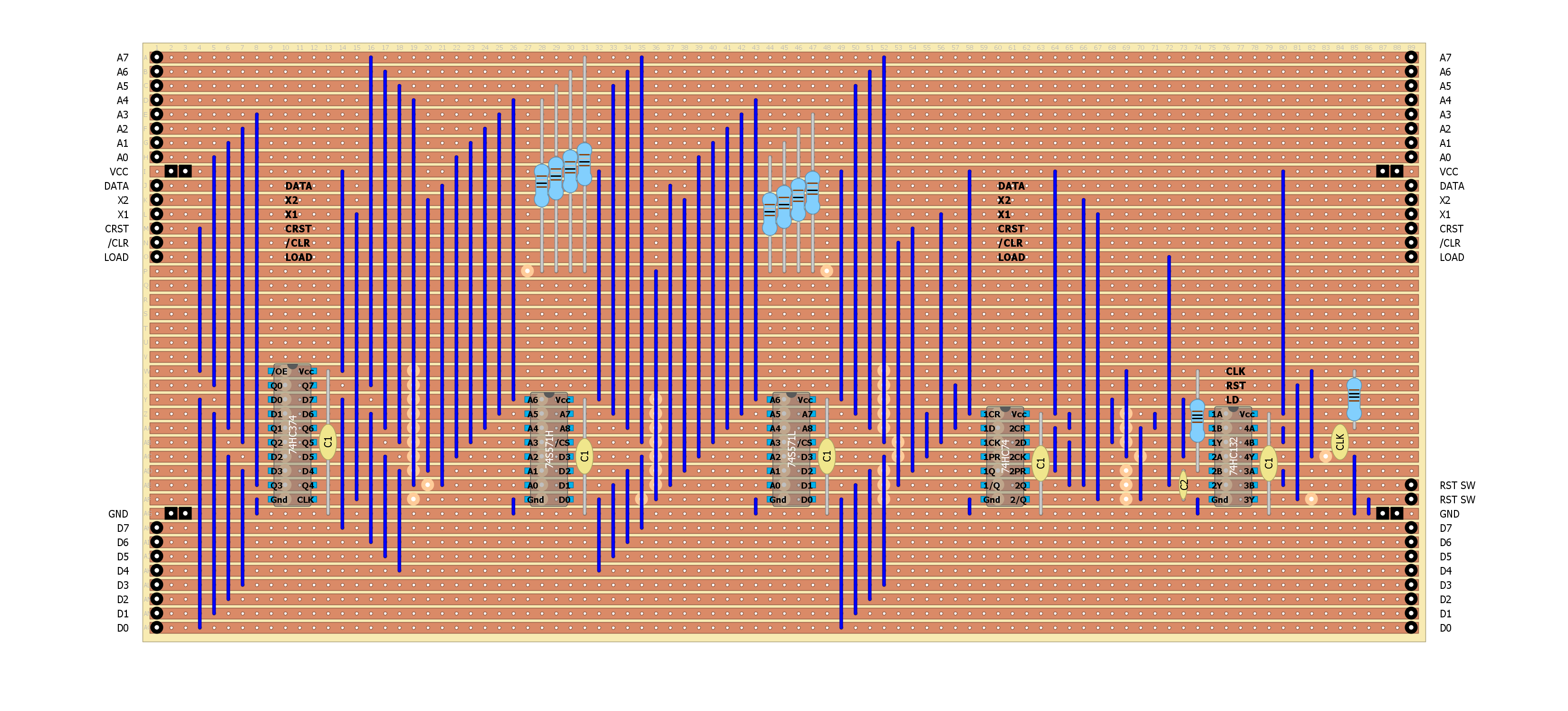
I made up a strip-board design for the 1 Bit CPU (2 bit memory version) using 74S571 PROMs (I have a couple spare). The design uses two boards stack on each other.
Here is the top board:
![]()
Here is the bottom board:
![]()
Each board will take about 4 to 5 hours to assemble.
---
I seem to have forgotten the power supply? I will fix it tomorrow.
AlanX
-
A Demonstration Program for a One Bit CPU
08/28/2017 at 14:59 • 0 commentsA Demonstration Program for a One Bit CPU
I was thinking about a suitable demonstration program for a one bit CPU.
My design has 4 inputs, two memory bits and 5 outputs.
Long time ago a friend had three 4PDT switches and two LEDs wired up to count the number of switches that were on. It was an interesting exercise to workout how he wired them up. Sounds like a great demonstration program for a one bit CPU, count the number of inputs that are switched on.
Well I started writing code with pencil and paper when I realised this is a logic minimisation problem.
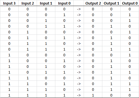
The Truth Table
Here is the truth table:
![]()
Here are the truth table equations:
C2 = A B C D;
C1 = A' B' C D + A' B C' D + A' B C D' + A' B C D + A B' C' D
   + A B' C D' + A B' C D + A B C' D' + A B C' D + A B C D';
C0 = A' B' C' D + A' B' C D' + A' B C' D' + A' B C D
   + A B' C' D' + A B' C D + A B C' D + A B C D';
The equations can be minimised (a little):
C2 = A B C D;
C1 = A C D' + A C' D + A' B C  + A B D' + B C' D + B' C D;
C0 = A B' C' D' + A' B C' D' + A' B' C D' + A B C D'
   + A' B' C' D + A B C' D + A B' C D + A' B C D;
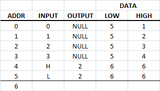
From the minimised equation I can now write the code directly. Here is the code to set C2 (Output 2) where A-D = Input 0-3:
![]()
I have not finished writing the code but it looks like about 80 lines of code.
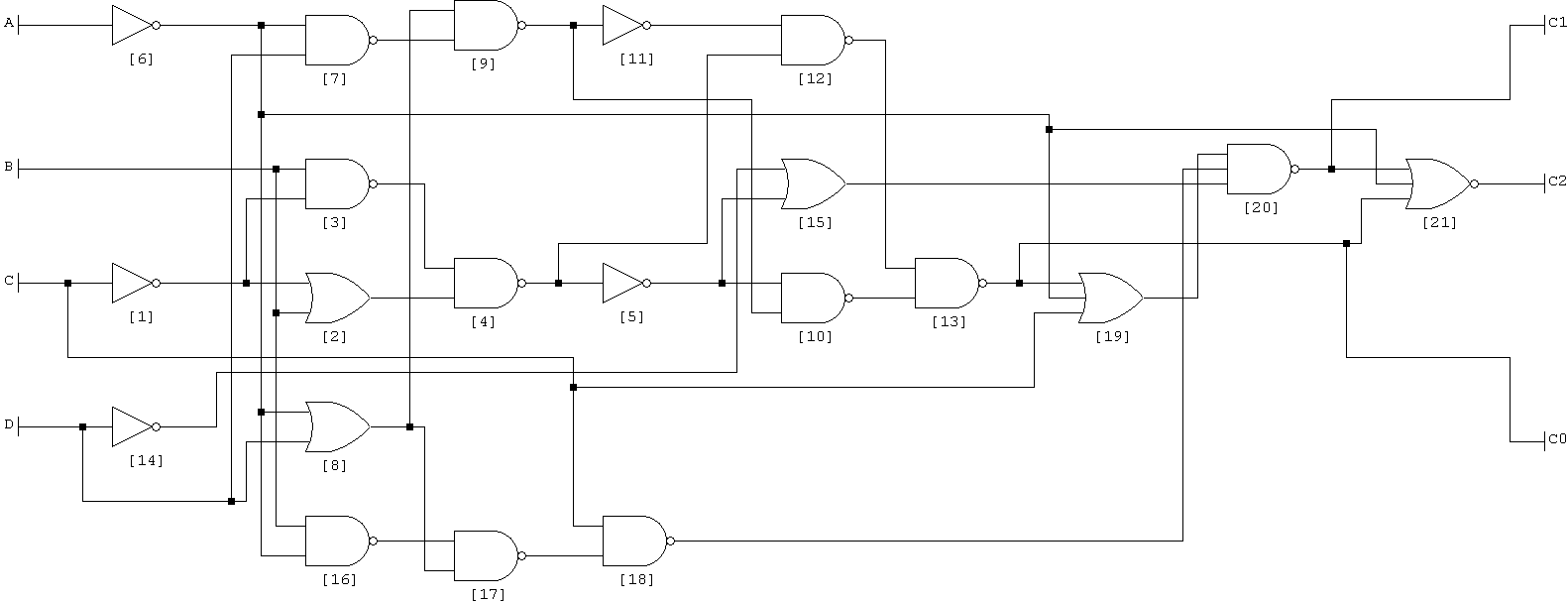
This is the schematic that Logic Friday came up with (scary!):
![]()
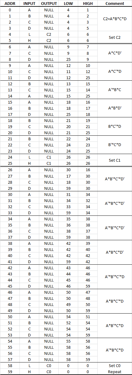
Completed ProgramThis morning I completed the code for the count program. Once you get the "hang" of the code it is pretty easy:
![]()
My coding approach is more finite state machine style, I did not use the memory bits.
Reworked the Simpler One Bit Version
I did not find any advantage in the more "complete" one bit CPU version. So I reworked the simpler version:
![]() (Note: The NAND gates are schmit triggers)
(Note: The NAND gates are schmit triggers)I dropped one of the memory bits as the programming style is more finite state machine (FSM) than procedural.
Now I will have to do a 5 bit count program! Here are the minimised truth table equations:
C2 = B C D E + A C D E + A B D E + A B C E + A B C D ;
C1 = A' B' C D E + A' B C' D E + A' B C D E' + A' B C D' E
   + B' C' D E + B' C D E' + B' C D' E + B C' D E' + A C' D E'
   + B C' D' E + A C' D' E + B C D' E' + A C D' E' + A B D' E';
C0 = A' B' C' D E' + A' B' C' D' E + A' B' C D' E'
   + A' B C' D' E' + A B' C' D' E' + A B' C' D E + A B' C D E'
   + A B' C D' E + A B C' D E' + A B C' D' E + A B C D' E'
   + A B C D E + A' B' C D E + A' B C' D E + A' B C D E'
   + A' B C D' E;
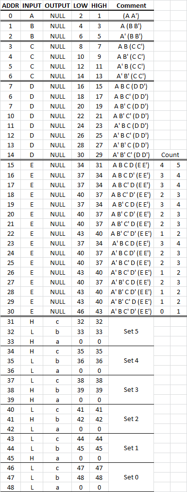
Now I can see the one limitation of the FSM approach - it does not scale very well. Here is the five switch version:
![]()
After searching the Internet, I found bit counting is a rather hard problem. Here is one solution for just 8 bits:
![]()
There are 93 two input NAND gates in the above drawing. So by program complexity is about right.
A Two Bit Adder
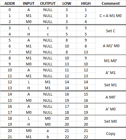
I looked at using an incrementer. It can be done in hardware or in software. Two options in software (1) finite state machine or (2) using memory bits. Here is a memory bit version:
![]()
Here are the equations (from Logic Friday):
c = A m1 m0;
s1 = A m1' m0 + m1 m0' + A' m1 ;
s0 = A m0' + A' m0;
So now I can count up to seven switches at a cost of 22 instructions per switch. An improvement on the 5 switch FSM version but not the 4 switch FSM version.
A Binary Tree Version
I reworked the five switch version using a binary decision tree:
![]()
A big improvement at 49 instructions.
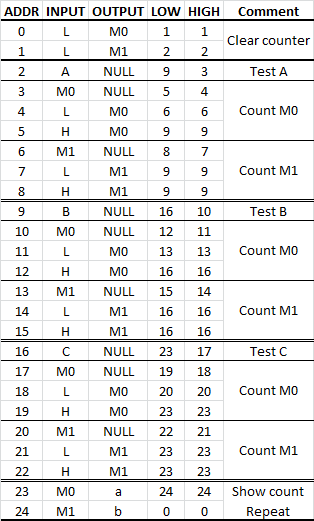
A Memory Bit Version
Using two memory bits and three switches (now 25 instructions):
![]()
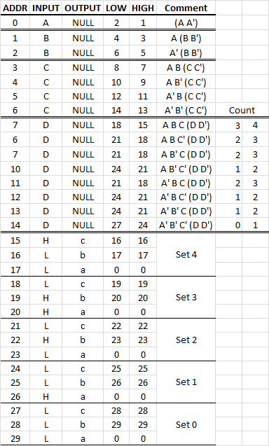
An finally a four switch binary tree version (30 instructions):
![]()
So although a truth table and logic minimisation will get you a solution that is easy to implement, hand crafted code will win if you put the time in.
Conclusion
Without memory or registers, the unavailability of subroutines and variables severely limits programming options. Coding density is also very low. If the problem can be modelled with truth table, a finite state machine, a programmable logic array or a decision tree then it may work well.
Adding memory and other hardware to improve the performance of a one bit CPU would make them of similar complexity of a four bit CPU. This limits the appeal of this approach.
The MC14500B with its ALU will have higher code density but will still suffers the same limitations as my ALU-less version.
Programming the One Bit CPU using logic equations is surprisingly easy. Here are the 2 bit adder logic equations:
- c = A m1 m0;
- s1 = A m1' m0 + m1 m0' + A' m1 ;
- s0 = A m0' + A' m0;
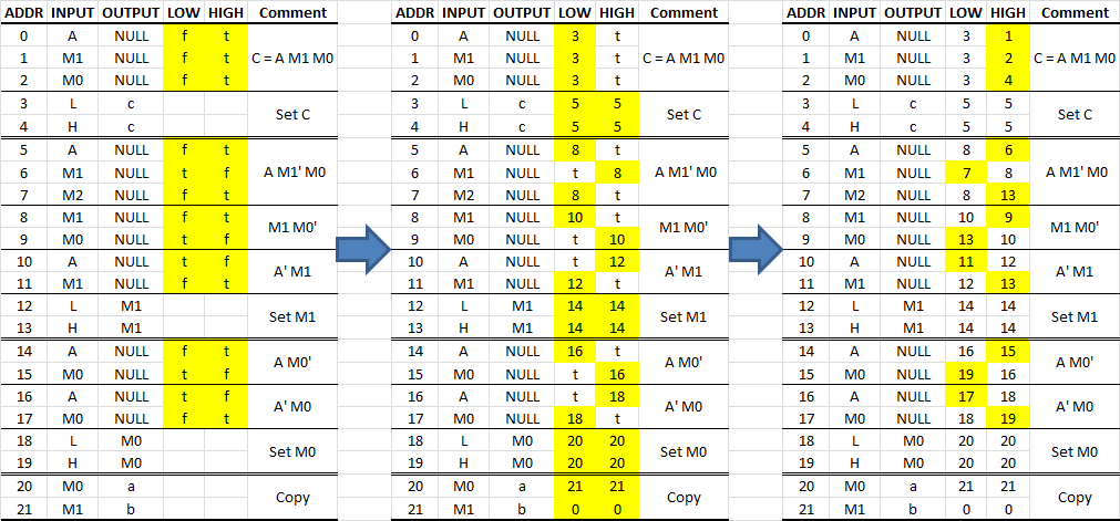
And the program code development steps:
![]()
The steps are:
- First create a truth table.
- Solve the logic equations (using Logic Friday).
- Populate the comments with the equations to model.
- Populated the true/false conditions with "t" of "f" (hi-lighted yellow in the first table above).
- Set the jump address for the false conditions which is usually the next logic equation block (hi-lighted yellow in the second table above).
- Set the next address for the true conditions (hi-lighted yellow in the third table above).
- Most of the code outputs to "NULL".
Regards AlanX
-
One Bit Block Diagram
08/27/2017 at 02:01 • 0 commentsOne Bit Block Diagram
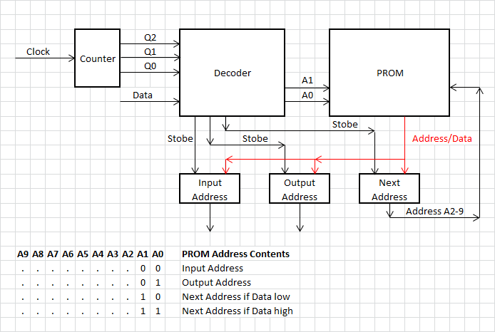
Here is a block diagram of the one bit CPU I want to design:
![]()
What I am doing different here is using the previously duplicated Input and Output addresses as separate Input and Output address. This gives 256 possible Inputs and 256 possible outputs instead of 16 inputs and 16 outputs. To do this a need a four phase clock and some decoder logic to select the correct Next Address (i.e. depending on if Data is low or Data is high).
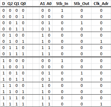
Truth Table
Here is the first pass truth table:
![]()
It first pass because small changes can make a bit difference to the decoder circuit.
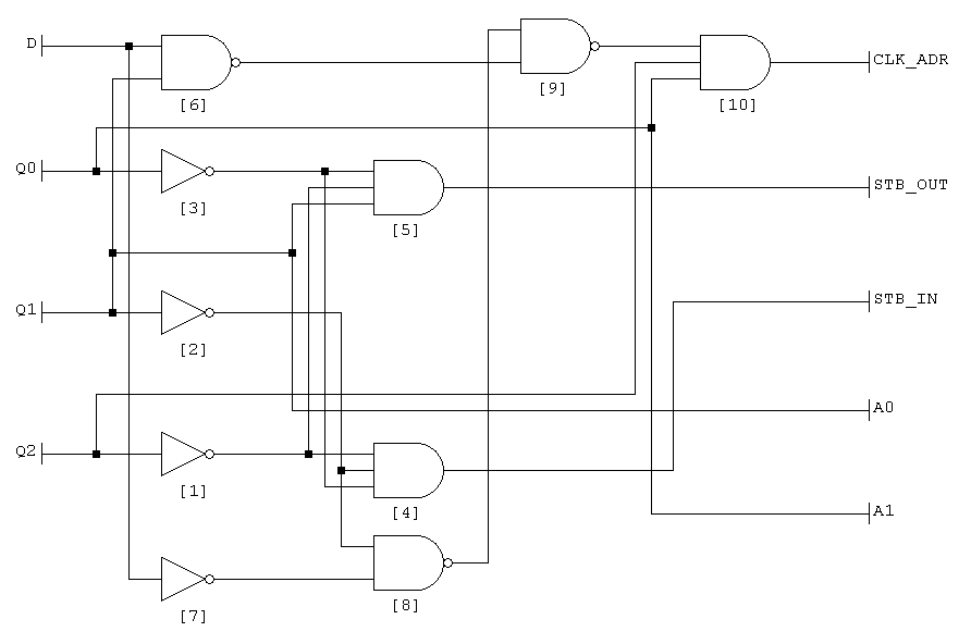
Here is the resulting circuit:
![]()
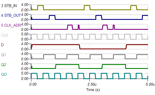
Testing the circuit in TinaTI (looking for glitches) and yes glitches were found on the CLK_ADR signal:
![]()
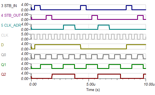
Playing around with the schematic and clocking the Data (D) signal, all good:
![]()
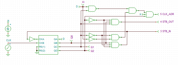
Here is the final schematic:
Ignore the inverter feeding into the CKA of the counter, it is only used to generate a "D" signal.
Conclusion
Is it worth the effort? The old design needed two chips, but not enough gates for the clock and reset logic, and this design needs four chips with enough gates left over for the clock and reset logic. The new design will also need an additional clocked latch for the input/output. So eight chips versus ten for a theoretically better system. The down side is that the improvements are unlikely to be used.
Here is the old design for reference:
![]()
Update
Reworked the decoder a little, it seems to be working as expected:
![]()
Regards AlanX
-
Flash RAM
08/26/2017 at 14:24 • 0 commentsFlash RAM
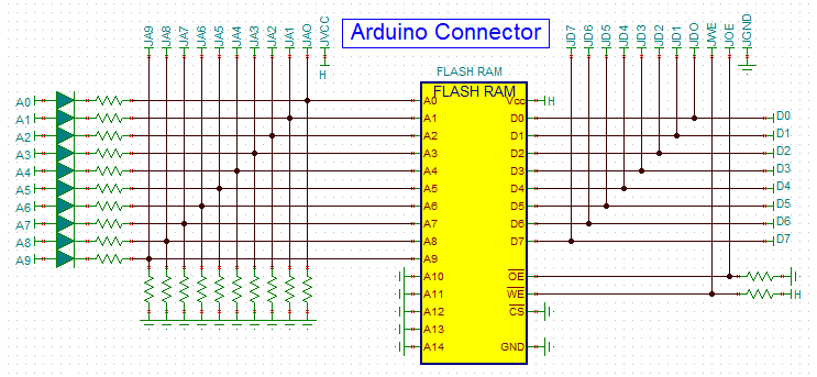
Nearly all computer projects need a ROM of some type. To date I have used PROMs. It works but the fear of making a mistake in the programming of the PROM, makes the process unpleasant. Enter the Flash RAM, re-programmable as if it was RAM (well nearly). Well actually they still need a programmer for simple systems. So I had a look at programming in-circuit. Here is a concept were an Arduino can be plugged in the "board" and the Flash RAM reprogrammed in-circuit:
![]()
The main problem here is that the diodes will slow down the normal operation of the Flash RAM.
Okay, how about a programmer? Unfortunately the Arduino does not have enough output pins. So we need a Mega 2560 or a port expander. Looking at port expanders four options are:
- use two Arduinos connected by an I2C bus
- use a PCF8574 port expander (which also uses an I2C bus)
- use a serial to parallel chip such as the 74HC595
- use a 74HC374 (a tri-state 8 x flip-flip)
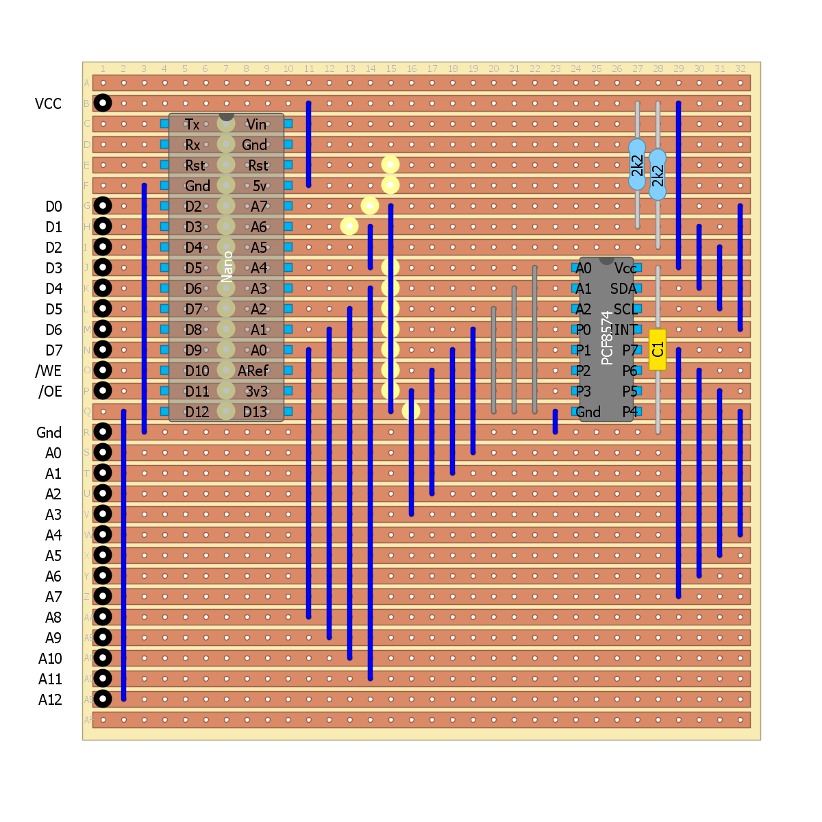
The PCF8574 has the advantage that the port is bi-directional, but this feature is not needed here. Here a strip-board version of the PCF8574:
![]()
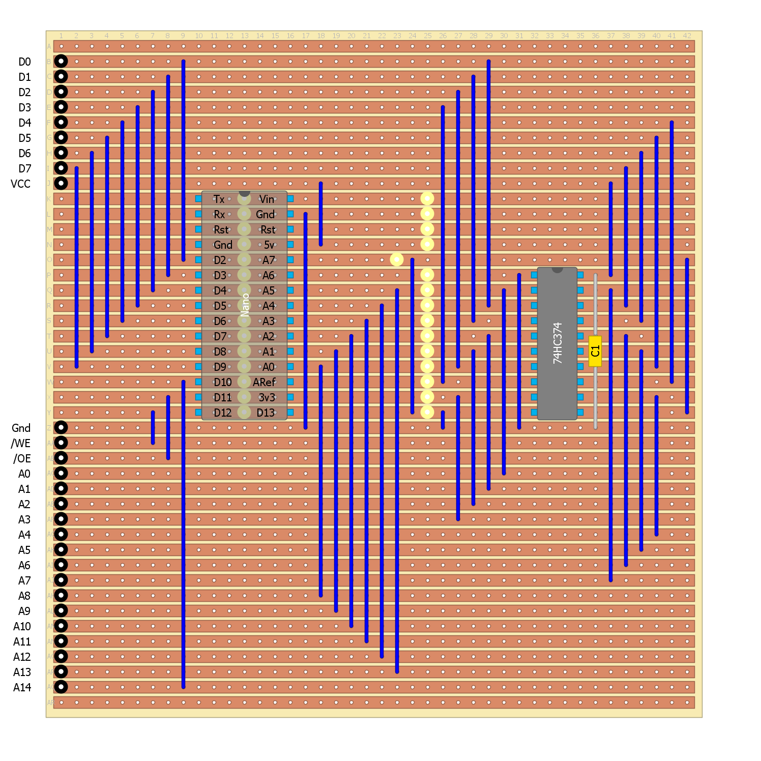
The other design of interest is the 74HC374:
![]()
The 74HC374 design will be much faster and has just enough outputs to fully program a 32k x 8 bit Flash RAM. So the clear winner.
Strip Board Programmer
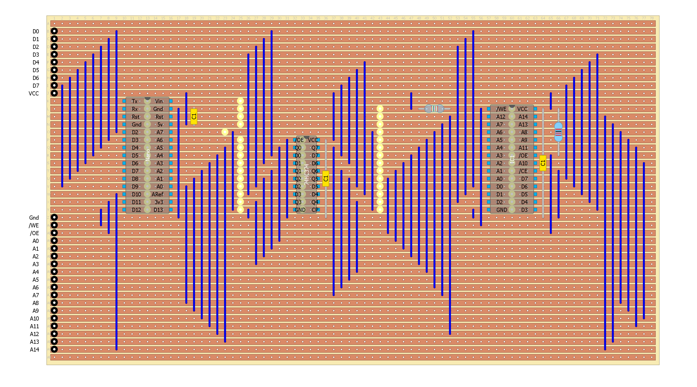
I knocked up a strip-board programmer:
![]()
While this is not too bad, it may make a good PCB project.
Memory Capacity
The other problem is the Nano memory capacity. To date I have been storing the programming data in code. The nano only has 32k Flash and we want to program a 32k Flash RAM. A bit of a tight fit! I suppose I could just program 50% at a time. The other options are to use a different Arduino product (a Mega 2650 for example) or to load the programming data from the serial console at program time (i.e. program the Flash RAM 64 bytes at a time as the data is received).
TBC ...
AlanX
-
The Laughton Electronics One Bit Machine
08/15/2017 at 07:11 • 0 commentsThe Laughton Electronics One Bit Machine
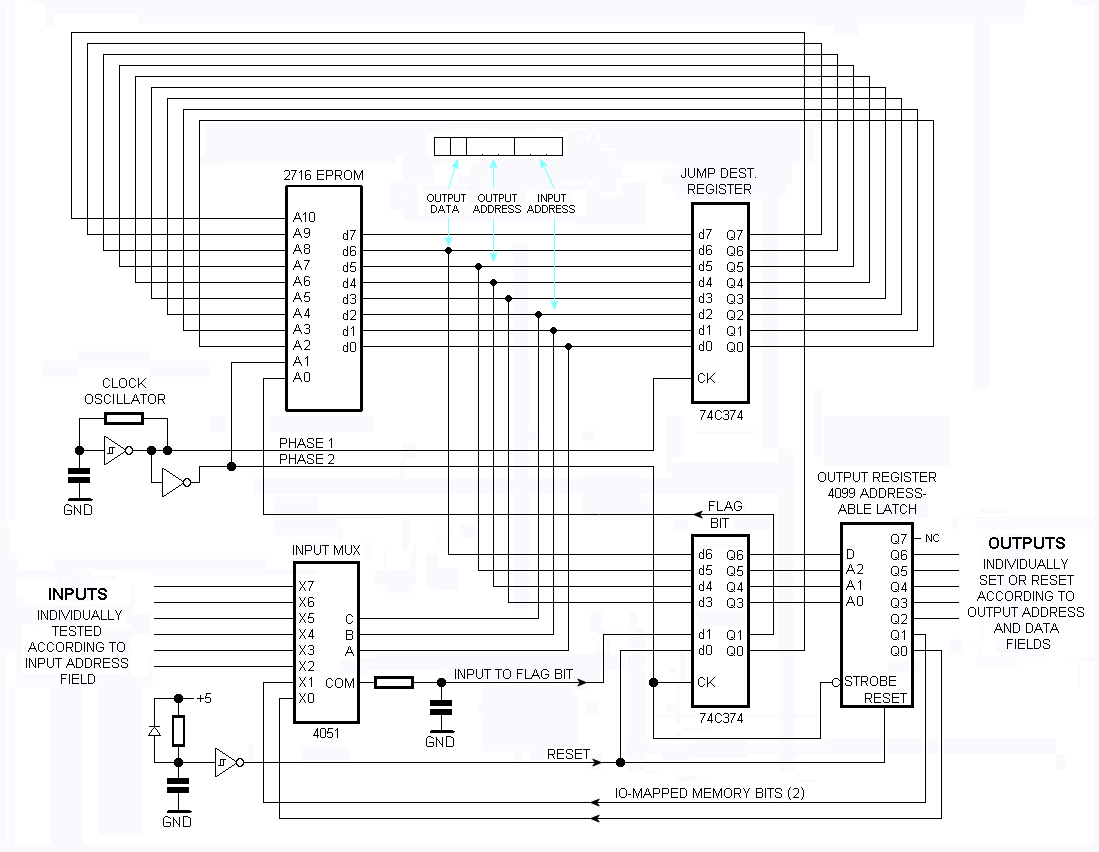
The Laughton Electronics one bit machine is very likely the smallest discrete CPU that can be built (http://laughtonelectronics.com/Arcana/One-bit%20computer/One-bit%20computer.html):
![]()
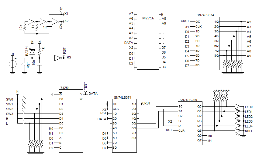
I have designed a simplified version that does not use the data bit in the instruction byte or requires the top half of the ROM to have jump on reset instructions:
![]()
(Don't build this, it is not final!)
The reset signal (RST) is clocked or synchronised (CRST) and turns off the address latch. The resistors set the reset address (0x00 in this case). As the clock is still running the instruction at the reset address is executed repeatedly.
My version will probably still need the deglitch (i.e. low pass) on the data line, (I am guessing that the ROM is generating address glitches).
I have taken a Subleq approach here and have a specific I/O address for Low and High. Like Laughton I have added two memory bits.
How does the memory addressing work?
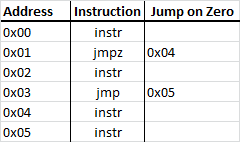
To understand the memory addressing consider typical set of instructions:
![]()
In the above, the next instruction (address) is automatically done in a hardware.
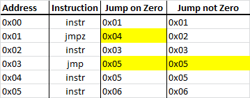
In the Laugthon machine there is no program counter so the next address must be explicit:
![]()
The cost is that the approach costs additional memory.
Here is the Laughton format:
![]()
You cannot actually change the input address based on the input bit (as it could oscillate) but you can change the output address. Really, to avoid programming difficulties (in your head!) it would be best to keep for both input bit cases, the input and output address the same. It would also simplify programming if one of the jump addresses is the preferred "next" address (say jump on one).
For my CPU, here is my programming template with some coding examples:
![]()
Note: Each row is a byte in ROM (merged cells are duplicated, so each instruction is 4 bytes.
You may see that a more sophisticated CPU would use the duplicated I/O address to extent the CPU I/O addresses and/or add OpCodes.
I am sure that many people look at the Laughton's machine (and download the image) but not knowing how to program it, just move on. The programming template makes it much more straight forward.
OpCode Density
The concept describes the amount of memory required to code something. Simple CPU usually have low OpCode density. Subleq for example is at least twice as bad as TTA (Transport Triggered Architecture), all other things being the same.
Laughton's machine has two functions or instructions and has a higher OpCode density than my version (which is pure TTA). The MC14500B has 16 instructions and the code density would be in the order of four times less ROM space than my machine.
So there is merit in considering an ALU in the bit path (at the cost of I/O addresses). For a single OpCode bit Laughton's approach is hard to beat.
Update
Spent half the day playing around with a strip-board version but decided I needed to get it working in TinaTi. Here is the working TinaTI schematic:
![]()
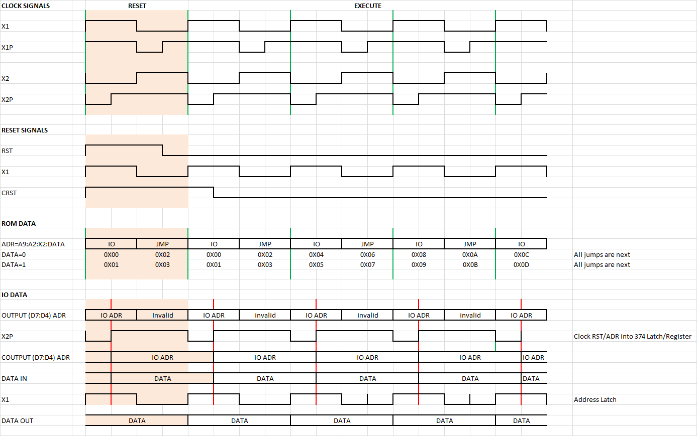
At the top is a hardware ROM! Most the work was getting the clock timing right for the reset. Here is the timing diagram:
![]()
Some thoughts on Laugthon's version. As it relies on slow ROM so it may not work with modern very fast PROMs. That is what the RC delay filter is for, to keep the data around so it can be clocked/latched. Anyway, in exchange for two additional chips, I don't have to program the top half of the PROM with reset instructions and the full IO address (8 bits) latched for the cycle. I was playing with a design that separated the two IO bytes but it was starting to get complicated. Overall, seven chips and a clock (i.e. eight chips) still makes a pretty small CPU.
A Second Update
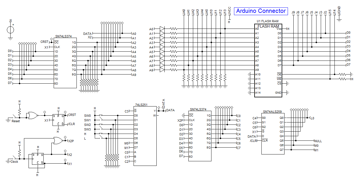
Further work but using a Flash RAM for the ROM. The idea here is to program the Flash RAM in-circuit with an Arduino. This schematic should work but further work is required:
![]()
This one bit CPU has 4 inputs, high (H), low (L) and two memory bits (M0 and M1). It has five outputs, null and the two memory bits. It has been tested in TinaTI except the 74LS259 model does not work.
If I build it then the thought shifts to what to use it for as a demonstration? One thought is a bit counter. That is to count the number of inputs pushed and to write the binary result.
AlanX
-
MC14500B and MC14500 Discrete Clone Timing
08/14/2017 at 08:17 • 0 commentsTiming
Ideally I would like the MC14500B and the MC14500 discrete clone to be compatible so that any circuit I build I can swap one out for the other.
I looked at the timing signals of the MC14500B and I find the WRITE (pulse) signal is probably too slow for modern memory (and even old memory) components. These two reference resorted to shaping the write pulse due to the issue:
- https://github.com/nicolacimmino/PLC-14500
- The Demonstration System from the MC14500B_Handbook.pdf
Although I did look at merging DIN and DOUT of the clone to single DATA signal as per the MC14500B, this is not really a great idea. The separate data paths are better as the DATA signal conflicts for the MC14500B (i.e. two common outputs during the timing cycle) with the muliplexed Input Data signal (if the WRITE signal is used for data multiplexing, which seems to be the way this signal is used). The conflict does not seem to worry the MC14500B but a current limiting resistor in the Input Data multiplexer signal line would seem to be a good idea.
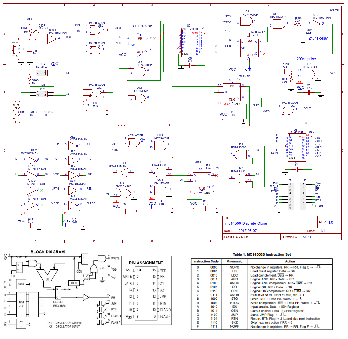
For the clone I have stayed with the full cycle WRITE signal (as opposed to the half cycle WRITE PULSE of the MC14500B) and added a separate /WP signal for the Data Output Addressable Latch.
Here is my schematic of the MC14500 Discrete Clone:
![]()
TBC ...
AlanX
-
Analysing the MC14500B Discrete Clone
08/12/2017 at 15:45 • 0 commentsPulling the MC14500B Discrete Clone apart and putting it back together
In case you have not seen it, here is the video demonstrating the MC14500B clone:
Here is the clone schematic:
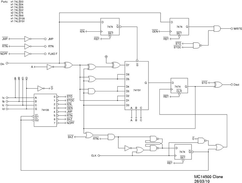
![]()
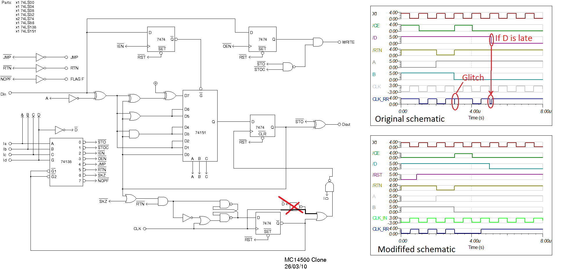
I have found that the clock logic is glitched and have edited the schematic:
![]()
The actual MC15400B has the instruction latched but this is only necessary if the ROM space is interlaced with the input or output address. The clone also differs in that the Data signal has been split into Din and Dout. This is actually more convenient. Finally NOPO 0 and FLAG 0 have not been decoded. The on board clock is also absent.
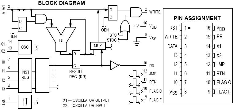
Here is the MC14500B block diagram and pin assignment for reference:
![]()
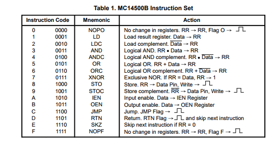
Finally here is the Instruction Set:
A working Example
Here is a working example of the MC14500B by Nicola Cimmino:
He has also put his schematic and other data on github:
![]()
(source: https://github.com/nicolacimmino/PLC-14500)
In this case, he uses an Arduino to program the SRAM.
---
And finally an ultra simple version where the operator is the ROM :(http://www.webalice.it/giussdp/cpu1bit/):
![]()
And his video and schematic:
![]()
AlanX
One Bit CPUs
I have been exploring one bit CPUs. For the right application they may be worth knowing.
 agp.cooper
 (Note: The NAND gates are schmit triggers)

