From the very beginning, the Y8 core is designed to allow extensive debugging features. Look at the early logs 3. Breakpoints ! and 4. The YGREC debug system to see the approach.
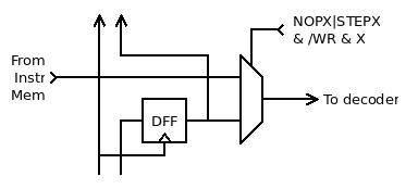
As the TAP system is being defined and implemented, more details emerge and here I describe one sub-sub-part of the debug system : the slice inserted between the instruction memory and the instruction decoder.

This DFF+MUX2 is pretty easy to design & layout, and the insertion delay is short enough, so why not add more features ?
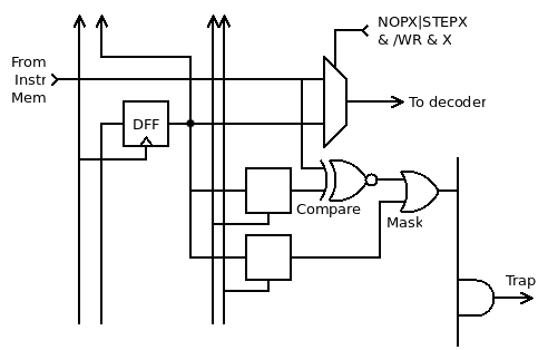
The early drafts promised a trap on a given instruction. This can be refined by masking some of the bits to compare and we get two registers (CoMPare and Match). Since latches uses 1/2 the size of DFF and we have a DFF very close, 2 latches are chosen.

This is very helpful during debugging because you don't have to focus on a particular instruction.
- Want to know how many times a given opcode is executed ?
- Want to know which instructions write to a give register ?
- Want to know why a given I/O register or range is overwritten ?
Just set the mask to select the desired field (opcode, register, immediate...) and select the behaviour (trap or count) and you're done.
Some more considerations and compromises...

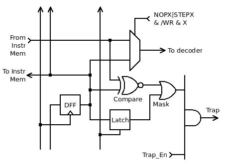
I dumped one latch to save space. That's the difference between 80 and 96 gates, in a core that is already quite small.
This means that the mask latch must be loaded first then another command loads the instruction chain again, and can't change it at all, so a specific command must also assert Trap_en only when /WR is high while sending a "START" command to the FSM.
The control logic is slightly more complex but the compactness matters. Fewer gates means fewer sources of errors, delay or power sinks.
Just added YGREC8_VHDL.20200730.tgz that includes the TAP/Slice circuit shown above.
 Yann Guidon / YGDES
Discussions
Become a Hackaday.io Member
Create an account to leave a comment. Already have an account? Log In.